EP1511180A1 - Distortion compensator - Google Patents
Distortion compensator Download PDFInfo
- Publication number
- EP1511180A1 EP1511180A1 EP02730842A EP02730842A EP1511180A1 EP 1511180 A1 EP1511180 A1 EP 1511180A1 EP 02730842 A EP02730842 A EP 02730842A EP 02730842 A EP02730842 A EP 02730842A EP 1511180 A1 EP1511180 A1 EP 1511180A1
- Authority
- EP
- European Patent Office
- Prior art keywords
- signal
- delay
- delay quantity
- limit value
- distortion compensation
- Prior art date
- Legal status (The legal status is an assumption and is not a legal conclusion. Google has not performed a legal analysis and makes no representation as to the accuracy of the status listed.)
- Granted
Links
Images










Classifications
-
- H—ELECTRICITY
- H04—ELECTRIC COMMUNICATION TECHNIQUE
- H04L—TRANSMISSION OF DIGITAL INFORMATION, e.g. TELEGRAPHIC COMMUNICATION
- H04L27/00—Modulated-carrier systems
- H04L27/32—Carrier systems characterised by combinations of two or more of the types covered by groups H04L27/02, H04L27/10, H04L27/18 or H04L27/26
- H04L27/34—Amplitude- and phase-modulated carrier systems, e.g. quadrature-amplitude modulated carrier systems
- H04L27/36—Modulator circuits; Transmitter circuits
- H04L27/366—Arrangements for compensating undesirable properties of the transmission path between the modulator and the demodulator
- H04L27/367—Arrangements for compensating undesirable properties of the transmission path between the modulator and the demodulator using predistortion
- H04L27/368—Arrangements for compensating undesirable properties of the transmission path between the modulator and the demodulator using predistortion adaptive predistortion
-
- H—ELECTRICITY
- H03—ELECTRONIC CIRCUITRY
- H03F—AMPLIFIERS
- H03F1/00—Details of amplifiers with only discharge tubes, only semiconductor devices or only unspecified devices as amplifying elements
- H03F1/32—Modifications of amplifiers to reduce non-linear distortion
- H03F1/3241—Modifications of amplifiers to reduce non-linear distortion using predistortion circuits
- H03F1/3247—Modifications of amplifiers to reduce non-linear distortion using predistortion circuits using feedback acting on predistortion circuits
-
- H—ELECTRICITY
- H03—ELECTRONIC CIRCUITRY
- H03F—AMPLIFIERS
- H03F1/00—Details of amplifiers with only discharge tubes, only semiconductor devices or only unspecified devices as amplifying elements
- H03F1/32—Modifications of amplifiers to reduce non-linear distortion
- H03F1/3241—Modifications of amplifiers to reduce non-linear distortion using predistortion circuits
- H03F1/3294—Acting on the real and imaginary components of the input signal
-
- H—ELECTRICITY
- H03—ELECTRONIC CIRCUITRY
- H03F—AMPLIFIERS
- H03F2200/00—Indexing scheme relating to amplifiers
- H03F2200/336—A I/Q, i.e. phase quadrature, modulator or demodulator being used in an amplifying circuit
-
- H—ELECTRICITY
- H03—ELECTRONIC CIRCUITRY
- H03F—AMPLIFIERS
- H03F2200/00—Indexing scheme relating to amplifiers
- H03F2200/468—Indexing scheme relating to amplifiers the temperature being sensed
-
- H—ELECTRICITY
- H03—ELECTRONIC CIRCUITRY
- H03F—AMPLIFIERS
- H03F2201/00—Indexing scheme relating to details of amplifiers with only discharge tubes, only semiconductor devices or only unspecified devices as amplifying elements covered by H03F1/00
- H03F2201/32—Indexing scheme relating to modifications of amplifiers to reduce non-linear distortion
- H03F2201/3233—Adaptive predistortion using lookup table, e.g. memory, RAM, ROM, LUT, to generate the predistortion
Definitions
- the present invention relates to a distortion compensation apparatus for use in a transmitter that transmits signals.
- the wireless system is often required to be small in size and to be operated with low electric power consumption.
- the wireless system using the linear modulation method requires a transmit circuit having a high linearity.
- a high output power amplifier (a power amplifier) is generally disposed at a last stage of the transmit circuit in the wireless system. Therefore, it is difficult to meet these requirements at the same time. That is to say, when the signal is amplified at a linear region of the high output power amplifier, the linearity is good, but the efficiency of the amplifier becomes poor. In this case, electric power consumption becomes high, which requires a large power source or makes heat dissipation conditions severe.
- a distortion compensation apparatus is used.
- the wireless system including the distortion compensation apparatus amplifies the signal in the non-linear region in the high output power amplifier to decrease the electric power consumption, and the distortion of the signal produced in the amplifier is compensated in the distortion compensation apparatus.
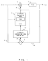
- Fig. 1 is an illustration for explaining a basic operation of a distortion compensation apparatus.
- the distortion compensation apparatus is in a digital pre-distortion type in this explanation. It is assumed that an input signal X (t) is processed at a processing unit 1, and is outputted as a signal Y (t).
- the distortion compensation apparatus detects or estimates the distortion produced at the processing unit 1, produces a compensation signal that compensates the distortion, and provides the compensation signal to the signal X (t).
- a subtraction circuit 11 produces an error signal 23 representing a difference between the reference signal 21 and the feedback signal 22.
- the reference signal 21 is not distorted, and is obtained by simply delaying the signal X (t) for a predetermined time.
- the feedback signal 22 is distorted at the processing unit 1. Accordingly, the error signal 23 corresponds to the distortion produced at the processing unit 1.
- a distortion compensation unit 12 comprises a table for storing information that produces a compensation signal 24.
- a distortion compensation signal updating unit 13 updates the table in the distortion compensation unit 12 based on the error signal 23.
- the distortion compensation unit 12 produces the compensation signal 24 based on the information extracted from the table using an amplitude or a power of the signal X (t) and the like as a search key.
- the compensation signal 24 cancels the error signal 23.
- a multiplier 14 multiplies the compensation signal 24 to the input signal X (t). Since the distortion produced at the processing unit 1 is compensated by the compensation signal 24, the signal Y (t) has no distortion (or suppressed distortion).
- a digital pre-distortion type distortion compensation apparatus in order to compensate the distortion adequately, a correct error signal 23 should be produced.
- the timing between the reference signal 21 and the feedback signal 22 should be matched accurately.
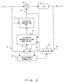
- a digital pre-distortion type distortion compensation apparatus generally comprises a delay unit 31 and a delay quantity control unit 32.
- the delay unit 31 delays the feedback signal.
- the delay quantity in the delay unit 31 follows instructions from the delay quantity control unit 32.
- the delay quantity control unit 32 calculates the delay quantity so that the timing between the reference signal 21 and the feedback signal 22 delayed in the delay unit 31 is matched, and notifies the result to the delay unit 31.
- a method of adjusting the timing between the signals i.e., a method of determining the delay quantity of the feedback signal
- ACLR Adjacent Channel Leakage Ratio
- the erroneous delay quantity is calculated at the delay quantity control unit 32.
- an incorrect error signal 24 is produced based on the erroneous delay quantity.
- the distortion cannot be compensated.
- the feedback system may be run away and the distortion may rather be increased. When such a situation occurs, the signal of an adjacent to channel may be adversely affected. Accordingly, it is desirable that the distortion compensation apparatus having the configuration described above have a protection function so that the delay quantity calculated in the delay quantity control unit 32 does not indicate an abnormal value.
- An object of the present invention is to provide a distortion compensation apparatus that can suppress distortion of a signal even if any fault occurs.
- the delay control means limits the delay quantity within a predetermined limit value.
- the delay quantity in the delay means has a value within the limited value, even if the reference signal or the feedback signal indicates an abnormal value. Accordingly, even if the reference signal or the feedback signal indicates an abnormal value, the feedback system for compensating the distortion of the signal does not run away, and the distortion is limited to the predetermined value or less.
- the limit value may be determined based on the temperature adjacent to the circuit for producing the second signal from the first signal, a period during which the transmitter has been used, and a pattern or patterns of the one or more carrier waves used for transmitting the second signal. This configuration allows an optimal limit value to be set depending on the environment under which the transmitter is used. The accuracy of the distortion compensation is expected to be improved.
- Fig. 3 shows an example of the environment under which the distortion compensation apparatus in one embodiment of the present invention is used.
- a base station device 40 of a mobile communication system sends and receives a radio signal to/from a mobile station 50.
- the base station device 40 comprises a transmitter 41 for transmitting the radio signal to the mobile station 50, and a receiver 42 for receiving the radio signal from the mobile station 50.
- the mobile station 50 is, for example, a mobile phone, and sends and receives the radio signal to/from the base station device 40.
- the mobile station 50 comprises a transmitter 51 for transmitting the radio signal to the base station device 40, and a receiver 52 for receiving the radio signal form the base station device 40.
- the distortion compensation apparatus of the embodiment is installed in the transmitter 41 or the transmitter 51.
- the distortion compensation apparatus of the present invention is not necessarily installed in the radio transmitter described above, and may be installed in an alternative transmitter.
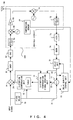
- Fig. 4 shows a distortion compensation apparatus in the embodiment.
- the distortion compensation apparatus is used in a transmitter for modulating and transmitting an input signal.
- the input signal is modulated by a quadrature modulator (QMOD) 61, and then is converted to an analog signal by a D/A converter (DAC) 62. After the analog signal passes through a frequency filter 63, a carrier wave is multiplied to the analog signal at a multiplier 64. The signal is further amplified by a power amplifier (PA) 65, and is transmitted via an antenna 66.
- QMOD quadrature modulator
- DAC D/A converter
- PA power amplifier
- the input signal produces distortion, when it is transmitted as described above.
- the distortion is produced mainly when the signal is amplified by the power amplifier 65.
- the signal amplified by the power amplifier 65 is branched in order to produce a feedback signal 22.
- a multiplier 71 converts the frequency of the signal.
- the signal passes through a frequency filter 72, and is converted into a digital signal by an A/D converter (ADC) 73.
- ADC A/D converter
- the digital signal is demodulated by a quadrature demodulator (QDEM) 74, and is delayed by the delay unit 31.
- a demodulation method of the quadrature demodulator 74 corresponds to a modulation method of the quadrature modulator 61.
- the feedback signal 22 is produced from the signal obtained by modulating and amplifying the input signal, as described above. Since the quadrature demodulator 74 corresponds to the quadrature modulator 61, the feedback signal 22 is the same signal as the input signal. However, the feedback signal 22 includes the distortion produced at an analog circuit 200 (mainly, the power amplifier 65). In addition, the feedback signal 22 is delayed from the input signal by the processing time of the feedback system.
- the subtraction circuit 11 produces the error signal 23 representing a difference between the reference signal 21 and the feedback signal 22.
- the reference signal 21 is obtained by delaying the input signal by a predetermined time using a fixed delay circuit 75.
- the delay time in the fixed delay circuit 75 is set longer than the processing time in the feedback system (the time herein means the time during which the input signal passes through the analog circuit 200 and returns to the subtraction circuit 11 minus the delay time by the delay unit 31).
- the distortion compensation unit 12 and the distortion compensation signal updating unit 13 are feasible by the existing arts, as described referring to Fig. 1. That is, the distortion compensation unit 12 comprises the table for storing information that produces the compensation signal 24.
- the distortion compensation signal updating unit 13 updates the table provided in the distortion compensation unit 12 based on the error signal 23.
- the distortion compensation unit 12 produces the compensation signal 24 based on the information extracted from the table using the amplitude or the power of the input signal and the like as a search key.
- the compensation signal 24 cancels the error signal 23.
- the multiplier 14 multiplies the compensation signal 24 to the input signal. Since the distortion produced at the analog circuit 200 (mainly, the power amplifier 65) is compensated by the compensation signal 24, the signal transmitted via the antenna 66 has no distortion (or suppressed distortion).
- a delay quantity control unit 81 calculates the delay quantity so that the timing between the reference signal 21 and the feedback signal 22 delayed in the delay unit 31 is matched (or minimizing the timing difference), and notifies the result to the delay unit 31.
- the delay quantity control unit 81 comprises a function to protect the transmitter from damage, when the reference signal 21 or the feedback signal 22 indicates an abnormal value caused by any type of damage.
- the distortion compensation apparatus in the embodiment comprises a temperature sensor 82 adjacent to the power amplifier 65.
- the delay quantity control unit 81 comprises a function to determine the delay quantity depending on the output of the temperature sensor 82.
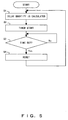
- Fig. 5 shows a schematic operation of a delay quantity control unit 81.
- the delay quantity is calculated so that the timing between the reference signal 21 and the feedback signal 22 delayed in the delay unit 31 is matched.
- the delay quantity is calculated by a method of utilizing the correlation between the above-mentioned signals, or ACLR (Adjacent Channel Leakage Ratio) . Based on the calculated delay quantity, the delay unit 31 is instructed.
- a timer is used to measure an elapsed time after the process of the step S1 is carried out.
- the elapsed time measured by the timer represents a period during which the process of the step S1 is carried out.
- Fig. 6 shows the delay quantity control unit 81.
- the delay quantity is determined using the correlation.
- the delay quantity control unit 81 comprises a correlation circuit 90 for determining correlation between the reference signal 21 and the feedback signal 22, and a control unit 100.
- the reference signal 21 and the feedback signal 22 comprise I-component signal and Q-component signal, respectively.
- the correlation circuit 90 performs complex multiplication between the I-component signal and the Q-component signal of the reference signal 21, and the I-component signal and the Q-component signal of the feedback signal 22.
- the signals complex multiplied are supplied to integrators 91a and 91b.
- the I-component signal and the Q-component signal of the feedback signal 22 are delayed by the delay unit 31.
- the delay unit 31 comprises FIR filters 111 and shift resistors 112.
- the integrators 91a and 91b integrate the supplied signals for a predetermined time period, respectively.
- Squarer units 92a and 92b square and output the integrated results from the integrators 91a and 91b.
- the outputs from the squarer units 92a and 92b are added by an adder, and are outputted as a "correlation value" between the reference signal 21 and the feedback signal 22.
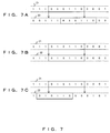
- the correlation circuit 90 is feasible by a known art. Therefore, further details on the configuration and the operation of the correlation circuit 90 is herein omitted, however, referring to Figs. 7A to 7C, the correlation value will be described in short.
- Fig. 7A shows the case that the feedback signal 22 lags from the reference signal 21. In this case, different data sets "010110” and “110101” are multiplied, and the correlation value becomes small.
- Fig. 7C shows the case that the feedback signal 22 leads over the reference signal 21. In this case, different data sets "010110” and "011000” are multiplied, and the correlation value becomes small.
- Fig. 7B shows the case that the timing between the feedback signal 22 and the reference signal 21 is matched. In this case, same data sets are multiplied, and the correlation value becomes great.
- Fig. 8 shows a relationship between the delay quantity at the delay unit 31 and the correlation value calculated by the correlation circuit 90.
- the correlation value between the reference signal 21 and the feedback signal 22 becomes great only when the timing of this pair of signals is matched.
- the timing difference between the reference signal 21 and the feedback signal 22 are adjusted by the delay quantity at the delay unit 31. Accordingly, if the delay quantity at the delay unit 31 is changed little by little to calculate the correlation value repeatedly, the results shown in Fig. 8 will be obtained. In this case, the timing at which the correlation value becomes a peak is detected as the timing between the reference signal 21 and the feedback signal 22 is matched.
- the control unit 100 calculates the delay quantity so that the timing between the reference signal 21 and the feedback signal 22 is matched according to the correlation value outputted from the correlation circuit 90.
- a delay timing control unit 101 determines the delay quantity in accordance with a predetermined algorithm or an instruction from a correlation value comparison processing unit 103, and notifies it to the delay unit 31. In this case, the delay unit 31 delays the feedback signal in accordance with the given instruction.
- the "delay quantity” includes data for instructing a shift quantity of the shift resistors 112 and/or data for instructing a TAP factor of the FIR filters 111.
- a correlation value store unit 102 holds the correlation value calculated by the correlation circuit 90.
- the "correlation value” is held in correspondence with the "delay quantity” instructed from the delay timing control unit 101 to the delay unit 31.
- the correlation value comparison processing unit 103 reads a plurality of "correlation values” held by the correlation value store unit 102, and gives an instruction to the delay timing control unit 101 based on a comparison result.
- Figs 9 and 10 are flowcharts showing a basic operation of the delay quantity control unit 81.
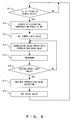
- Fig. 9 is a flowchart showing a processing for roughly determining the delay quantity.
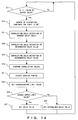
- Fig. 10 is a flowchart showing a processing for sufficiently and finely adjusting the delay quantity determined by the processing shown in Fig. 9.
- the processing shown in Fig. 9 is not necessarily carried out repeatedly, but may be carried out only upon an initial operation.
- the delay quantity control unit 81 carries out the processing for determining the delay quantity at a predetermined interval.
- steps S12 to S18 are carried out.
- step S12 updating the table provided at the distortion compensation unit 12 is stopped.
- step S13 a "lower limit value" is notified to the delay unit 31 as the delay quantity.
- the delay unit 31 delays the feedback signal by the time corresponding to the lower limit value.
- the lower limit value is stored in a limit value holding unit 104.
- the correlation value between the reference signal 21 and the feedback signal 22 is calculated.
- the correlation value calculated is held at the correlation value store unit 102.
- the delay quantity is incremented, and the delay quantity incremented is checked whether or not it reaches an "upper limit value.”
- the correlation value is again calculated back to the step S14.
- the “increment” herein means that the delay quantity in the delay unit 31 is allowed to be increased by one clock timing of the shift resistors 112.
- the maximum correlation value among them is selected in a step S17.
- the delay quantity at the timing of the maximum correlation value is obtained is detected, and the detected delay quantity is notified to the delay unit 31. Thereafter, updating the table of the distortion compensation unit 12 is restarted.
- the correlation value is calculated at the current delay quantity (a shift quantity of the shift resistors 112, and the TAP factor of the FIR filters 111).
- the current delay quantity is incremented to calculate the correlation value.
- the current delay quantity is decremented to calculate the correction value.
- the increment/decrement of the delay quantity are performed by changing the TAP factor of the FIR filters 111. It is possible to more finely adjust the delay quantity by the method of changing the TAP factor of the FIR filters 111 than with the method of changing the shift quantity of the shift resistors 112.
- step S24 there is detected the delay quantity by which the maximum correlation value among three correlation values obtained in the steps S21 through S23 is obtained.
- step S25 the detected delay quantity is checked whether or not it exceeds "the limit value.”
- the limit value herein means the upper limit value or the lower limit value as described above.
- the phrase "the delay quantity exceeds the limit value” means that "the delay quantity exceeds the upper limit value” or "the delay quantity is lower than the lower limit value.”
- the delay quantity is set in the delay unit 31 in step S26.
- the limit value (the upper limit value or the lower limit value) is set in the delay unit 31 in step S27. Thereafter, updating the table of the distortion compensation unit 12 is restarted.
- the limit value is set in the delay unit 31. Consequently, the delay quantity set in the delay unit 31 is always within a range from "the lower limit value” to "the upper limit value.”
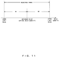
- Fig. 11 is an illustration for explaining the limit value.
- the limit value includes the upper limit value and the lower limit value, as described above.
- the upper limit value and the lower limit value may be directly designated, and may be designated by the reference value and the distance from the reference value (W1 and W2), respectively. In the latter case, the distance W1 and the distance W2 may be the same, or may be different.
- the limit value is basically determined before the transmitter is shipped (i.e., determined in the production factory). In this case, the limit value may be determined by a simulation and the like, or may be determined actually using the transmitter and transmitting the signal. The limit value may be determined so that a distortion property (for example, ACLR property) satisfies a predetermined standard. When the transmitter can transmit the signal by selecting an arbitrary pattern from a plurality of carrier patterns, the limit value may be determined so that the distortion property satisfies the predetermined standard if the signal is transmitted in the pattern that utilizes the broadest band among the plurality of patterns. The reason is as follows: In the distortion compensation apparatus shown in Fig.
- the limit value of the delay quantity in the delay unit 31 (the delay quantity to delay the feedback signal 22) may be set as a fixed value, but may be dynamically adjusted depending on an external environment or a communication environment.
- the method of changing the limit value based on the temperature in the transmitter, the service period (aged deterioration) of the transmitter, and the carrier pattern when the transmitter transmits the signal is described below.
- the delay time of the signal in the analog circuit 200 depends on the temperature. Accordingly, the time duration from the input signal is inputted to the feedback signal 22 corresponding to the input signal is supplied to the subtraction circuit 11 depends on the temperature. Thus, it is desirable that the limit value of the delay quantity in the delay unit 31 is adjusted based on the temperature around the analog circuit 200.
- the temperature around the analog circuit 200 is detected by the temperature sensor 82, and is notified to the delay quantity control unit 81.
- Fig. 12A is a schematic view showing a table into which a corresponding relationship between a temperature and a delay quantity is registered.
- This table corresponds to the limit value holding unit 104 provided in the delay quantity control unit 81. It is assumed that the temperature-dependence of the delay time of the signal at the analog circuit 200 is known. The limit value at each temperature is generated in advance in accordance with the temperature property. However, if the temperature dependency of the delay time of the signal at the analog circuit 200 can be represented by a mathematical expression, the temperature around the analog circuit 200 is detected, from which the limit value may be calculated. In this case, it is not needed to create the table in advance.
- Fig. 13 is a flowchart of a processing for determining the delay quantity referring to the temperature.
- the basic operation for referencing the temperature is the same as the procedure shown in Fig. 10.
- the delay quantity where the greatest correlation value is obtained is detected in the step S24, and then the temperature around the analog circuit 200 is detected in step S31.
- the temperature is detected using the temperature sensor 82.
- the limit values (including the upper and the lower limit values) corresponding to the detected temperature is set.
- the limit values corresponding to the detected temperature may be extracted from the table shown in Fig. 12A, or may be calculated using the mathematical expression defined in advance.
- the processing for notifying the delay quantity determined based on the determination result to the delay unit 31 is the same as explained referring to Fig. 10.
- this method allows the optimum limit value to be set dynamically depending on the environment under which the transmitter is used.
- Fig. 14 is a flowchart of a processing for determining the delay quantity referring to the service period of the transmitter. Basically, the operation is the same as the procedure explained referring to Fig. 13 except that steps S41 and S42 are performed instead of the steps S31 and S32.
- the service period of the transmitter is detected.
- the service period of the transmitter is, for example, measured by a timer and the like that is activated when the transmitter is started to be used.
- the limit value corresponding to the service period detected is set.
- the limit value corresponding to the service period of the transmitter may be extracted from the table shown in Fig. 12B, or may be calculated using a mathematical expression defined in advance.
- aged deterioration properties of respective units in the transmitter are known.
- Fig. 15 shows a multiple carrier transmitter comprising one embodiment of a distortion compensation apparatus.
- the transmitter can multiplex and transmit four signals.
- base band signals are inputted via channels CH1 to CH4, frequency converting units 121 multiply periodic waves having frequencies ( ⁇ 1 to ⁇ 4) corresponding to respective base band signals.
- the respective base band signals are allocated at different frequency bands.
- These signals are synthesized by a synthesizer 122, and guided to the quadrature modulator (QMOD) 61.
- QMOD quadrature modulator
- the transmitter shown in Fig. 15 can allocate plural input signals at different frequency bands and multiplex them.
- the basic configuration and the basic operation of the distortion compensation apparatus, the modulation circuit and the analog circuit are the same as explained referring to Fig. 4.
- the frequency bands to be used are also changed.
- different frequency bands are used in the case where CH1 and CH2 are multiplexed and in the case where CH3 and CH4 are multiplexed.
- a combination of the frequency band used is hereinafter referred to as the carrier pattern.
- the optimal value of the delay quantity to be set in the delay unit 31 becomes uniform irrespective of the carrier pattern as long as the signal delay property in the analog circuit 200 does not depend on the frequency.
- the signal delay may be frequency-dependent in the analog circuit. Consequently, the optimal value of the delay quantity to be set in the delay unit 31 will be changed in accordance with the carrier pattern.
- Fig. 16 shows a relationship between a carrier pattern and an optimal delay quantity.
- Fig. 16 as example 1, only one signal is transmitted, and as example 2, two channels or four channels are multiplied. In either case shown in Fig. 16, when higher frequency bands are used, the optimal delay quantity is increased.
- the limit values (including the upper and lower limit values) for limiting a variable range of the delay quantity be changed in accordance therewith as shown in Fig. 17.
- the distortion compensation apparatus in this embodiment comprises a function of changing the limit value of the delay quantity in accordance with the carrier pattern.
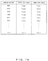
- Fig. 18 is a schematic view showing a table into which a corresponding relationship between a carrier pattern and a limit value of a delay quantity is registered.
- the table corresponds, for example, to the limit value holding unit 104 provided in the delay quantity control unit 81.
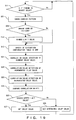
- Fig. 19 is a flowchart of a processing for determining a delay quantity referring to a carrier pattern. Basically, the processing is the same as the procedure explained referring to Fig. 10 except that steps S51 and S53 are performed before executing the steps S12 to S27, if the carrier pattern is referenced.
- the present carrier pattern is checked. In other words, it determines which channel is used among the channels CH1 to CH4. The information whether or not respective channels are used is notified from a higher-level control apparatus (not shown) disposed within the transmitter to the delay quantity control unit 81.
- a step S52 it determines that the present carrier pattern is changed or not changed from the carrier pattern performed when the processing shown in the flowchart was performed previously.
- the limit values including the upper and lower limit values
- the limit values corresponding to the new carrier pattern is extracted from the table shown in Fig. 18 and is held.
- the delay quantity to be set in the delay unit 31 is calculated in the steps S21 to S24, and the delay quantity is compared with the limit value obtained in the steps S51 to S53.
- the delay quantity is set in the delay unit 31 as it is.
- the limit value is set in the delay unit 31 instead of the calculated delay quantity.
- this method allows the preferable limit value to be always used dynamically even if the carrier pattern is changed in the multiple carrier transmitter.
- the width of the limit value may be uniform to all carrier patterns as shown in Fig. 17, or may be changed in accordance with the carrier patterns as shown in Fig. 20. In the latter case, for example, when the band width used for transmitting the signal is increased, the width of the limit value may be decreased, or when the band width used for transmitting the signal is decreased, the width of the limit value may be increased. Specifically, in the central pattern of the five carrier patterns shown in example 2 of Fig. 16, the width of the limit value is set to be narrow. In the pattern at the right or left end, the width of the limit value is set to be wide.
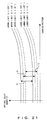
- the limit value of the delay quantity may be set taking both the temperature and the carrier pattern into consideration.
- a limit value range A when the temperature around the power amplifier 65 is at 55 degrees is drawn by a solid line
- a limit value range B when the temperature is at 25 degree is drawn by a waved line
- a limit value range C when the temperature is at 5 degrees below zero is represented by a two-point chain line.
- the limit value is set for the delay quantity that should be notified to the delay unit 31, as described above.
- the delay quantity calculated utilizing the correlation between the reference signal 21 and the feedback signal 22 exceeds the limit value, it is recognized that any damage may be produced, and the limit value is notified to the delay unit 31 instead of the delay quantity calculated. Accordingly, if any abnormality is produced in the reference signal 21 or the feedback signal 22, the distortion compensation apparatus does not run away, and the distortion produced in the transmitted signal can be suppressed to the predetermined value or less.
- the delay quantity calculated will be notified to the delay unit 31 as it is, as long as the delay quantity calculated does not exceed the limit value. However, even if the damage is not actually produced, the delay quantity can approach temporarily the limit value. In this case, it is desirable that the delay quantity be converged to the optimal delay quantity in a short time.
- the function to converge the delay quantity to the optimal delay quantity in a short time when the delay quantity calculated utilizing the correlation between the reference signal 21 and the feedback signal 22 approach the limit value.
- the distortion compensation apparatus described below performs the processing for adjusting the delay quantity at a predetermined cycle under the normal operation, as explained referring to Fig. 5.
- the "predetermined cycle” herein means about, for example, several minutes to several tens of minutes.
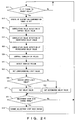
- the delay quantity is adjusted at every predetermined cycle by performing the flowchart shown in Figs. 9 and 10.
- the unit time incremented in the step S22 and the unit time decremented in the step S23 are about, for example, several tens of pico seconds under the normal operation.
- the unit time corresponds to the magnitude of the change in the delay quantity at one processing for adjusting the delay quantity, and therefore is hereinafter called "adjustment step size.”
- Fig. 22 is a flowchart of a processing for determining a delay quantity while changing a frequency of carrying out a delay quantity adjusting processing.
- this flowchart includes the procedure of increasing the frequency to carry out the processing for adjusting the delay quantity, i.e., the procedure of shortening the cycle for performing the processing for adjusting the delay quantity, when the delay quantity to be notified to the delay unit 31 approaches the limit value.
- the procedure is as follows:
- steps S61 and S62 are carried out.
- step S61 it is determined that the delay quantity notified to the delay unit 31 is or is not within the frequency change range.
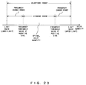
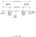
- the frequency change range is within the adjustment range defined by a set of limit values as shown in Fig. 23, and means the predetermined range adjacent to each limit value.
- the frequency change range is constituted by the range from "a frequency threshold value at positive side” to "the upper limit value” and the range from "a frequency threshold value at negative side” to "the lower limit value.”
- the limit value is notified to the delay unit 31. In this case, it may be estimated that the delay quantity which is notified to the delay unit 31 is within the frequency change range.
- the frequency of performing the processing for adjusting the delay quantity shown in the steps S21 to S27 is changed. Specifically, the time-out period of the timer is shortened, as explained referring to Fig. 5. In this case, the time-out period that is changed from about several minutes to several tens of minutes in the normal operation into several seconds to several tens of seconds. The period from the time to perform the processing for adjusting the delay quantity this time to the time to perform the processing for adjusting the delay quantity next time will be shortened as compared with that under the normal operation. Accordingly, if the delay quantity calculated is changed temporarily, the delay quantity to be notified to the delay unit 31 is expected to be converged to the optimal delay quantity in a short time.
- Fig. 24 is a flowchart of a processing for determining a delay quantity by changing a step size in a delay quantity adjusting process.
- a step S71 it is determined that the delay quantity notified to the delay unit 31 is or is not within a step size change range.
- the step size change range is constituted by the range from "a step size threshold value at positive side” to "the upper limit value” and the range from "a step size threshold value at negative side” to “the lower limit value.”
- the step size threshold value may be the same or different as/from the frequency threshold value as described above.
- the adjustment step size is changed. Specifically, the adjustment step size used in the steps S22 and S23 is increased. In this case, the adjustment step size that is set to about several tens of pico seconds under the normal operation is changed to about several hundreds pico seconds. The adjustment step size in the processing for adjusting the delay quantity next time will be increased as compared with that under the normal operation. Accordingly, when the delay quantity calculated is changed temporarily, the delay quantity to be notified to the delay unit 31 is expected to be converged to the optimal delay quantity in a short time.
- the timing between the reference signal and the feedback signal is matched by adjusting the delay quantity of the feedback signal.
- the delay quantity of the reference signal is adjusted, it is also required to delay some signals including the signals supplied from the distortion compensation unit 12 to the distortion compensation signal updating unit 13.
- a set of limit values (including the upper and lower limit values) are used to limit the setting range of the delay quantity.
- the present invention is not limited thereto, and may be applicable to the configuration that only one of the upper and lower limit values is used.
Landscapes
- Engineering & Computer Science (AREA)
- Physics & Mathematics (AREA)
- Nonlinear Science (AREA)
- Power Engineering (AREA)
- Computer Networks & Wireless Communication (AREA)
- Signal Processing (AREA)
- Amplifiers (AREA)
- Transmitters (AREA)
Abstract
Description
Claims (12)
- A distortion compensation apparatus used in a transmitter that produces and outputs a second signal from a first signal, comprising:wherein said delay control means limits the delay quantity within a predetermined limit value.delay means for delaying a feedback signal obtained from by the second signal; anddelay control means for determining a delay quantity of said delay means so that a timing difference between a reference signal obtained from the first signal and the feedback signal delayed by said delay means is made small,
- The distortion compensation apparatus according to claim 1,
wherein a circuit that produces the second signal from the first signal comprises an amplifier. - The distortion compensation apparatus according to claim 1, further comprising
temperature detecting means for detecting a temperature adjacent to the circuit that produces the second signal from the first signal, wherein
said delay control means determines the limit value based on the temperature detected by said temperature detecting means. - The distortion compensation apparatus according to claim 1, further comprising
timer means for measuring a period during which the transmitter is used, wherein
said delay control means determines the limit value based on the period during which the transmitter is used. - The distortion compensation apparatus according to claim 1, further comprising
frequency adjusting means for adjusting a frequency of carrying out a process that said delay control means determines the delay quantity, wherein
when the delay quantity exceeds a certain threshold and approaches the limit value, the frequency of carrying out the process that said delay control means determines the delay quantity is made higher than that in the case where the delay quantity does not exceed the threshold. - The distortion compensation apparatus according to claim 1, further comprising
adjusting means for gradually changing the delay quantity when the delay quantity is changed, wherein
when the delay quantity exceeds a certain threshold and approaches the limit value, said adjusting means for changing the delay quantity increases the change quantity as compared with that in the case where the delay quantity does not exceed the threshold. - The distortion compensation apparatus according to claim 1, wherein the limit value is determined under the condition that the transmitter uses a maximum band available for transmitting the signal and transmits the signal.
- The distortion compensation apparatus according to claim 1, wherein the limit value is determined so that distortion properties of the signal transmitted from the transmitter satisfy a predetermined standard.
- A distortion compensation apparatus used in a transmitter that produces and outputs a second signal from a first signal using one or more carrier waves, comprising:wherein said delay control means limits the delay quantity within a predetermined limit value, and wherein the limit value is determined based on a pattern or patterns of the one or more carrier waves used for transmitting the second signal.delay means for delaying a feedback signal obtained from the second signal; anddelay control means for determining a delay quantity of said delay means so that a timing difference between a reference signal obtained from the first signal and the feedback signal delayed by said delay means is made small,
- A distortion compensation apparatus used in a transmitter that produces and outputs a second signal from a first signal, comprising:wherein said delay control means limits the delay quantity within a predetermined limit value.delay means for delaying the first signal to produce a reference signal; anddelay control means for determining a delay quantity of said delay means so that a timing difference between the reference signal and a feedback signal obtained from the second signal is made small,
- A distortion compensation apparatus used in a transmitter that produces and outputs a second signal from a first signal, comprising:wherein said delay control means limits the delay quantity within a predetermined limit value.delay means for delaying a reference signal obtained from the first signal and a feedback signal obtained from the second signal; anddelay control means for determining a delay quantity of said delay means so that a timing difference between the reference signal and the feedback signal is made small,
- A transmitter for producing and outputting a second signal from a first signal, comprising:production means for producing the second signal from the first signal;delay means for delaying a feedback signal obtained from the second signal;delay control means for determining a delay quantity of said delay means so that a timing difference between a reference signal obtained from the first signal and the feedback signal delayed by said delay means is made small; andlimiting means for limiting the delay quantity within a predetermined limit value.
Applications Claiming Priority (1)
| Application Number | Priority Date | Filing Date | Title |
|---|---|---|---|
| PCT/JP2002/005371 WO2003103165A1 (en) | 2002-05-31 | 2002-05-31 | Distortion compensator |
Publications (3)
| Publication Number | Publication Date |
|---|---|
| EP1511180A1 true EP1511180A1 (en) | 2005-03-02 |
| EP1511180A4 EP1511180A4 (en) | 2006-02-15 |
| EP1511180B1 EP1511180B1 (en) | 2011-03-09 |
Family
ID=29606643
Family Applications (1)
| Application Number | Title | Priority Date | Filing Date |
|---|---|---|---|
| EP02730842A Expired - Lifetime EP1511180B1 (en) | 2002-05-31 | 2002-05-31 | Distortion compensator |
Country Status (4)
| Country | Link |
|---|---|
| EP (1) | EP1511180B1 (en) |
| JP (1) | JP3866746B2 (en) |
| DE (1) | DE60239426D1 (en) |
| WO (1) | WO2003103165A1 (en) |
Cited By (1)
| Publication number | Priority date | Publication date | Assignee | Title |
|---|---|---|---|---|
| EP2221962A1 (en) * | 2009-02-05 | 2010-08-25 | Fujitsu Limited | Predistorter and distortion compensation method |
Families Citing this family (5)
| Publication number | Priority date | Publication date | Assignee | Title |
|---|---|---|---|---|
| JP4961661B2 (en) | 2004-09-10 | 2012-06-27 | 株式会社日立製作所 | Digital predistortion type transmitter and radio base station |
| CN101228690B (en) * | 2005-07-29 | 2010-08-18 | 富士通株式会社 | delay adjustment device |
| JP2007318298A (en) * | 2006-05-24 | 2007-12-06 | Stack Denshi Kk | Distortion compensation circuit |
| JP5034319B2 (en) * | 2006-05-26 | 2012-09-26 | 富士通株式会社 | Distortion compensation apparatus and distortion compensation method |
| JP2008205759A (en) * | 2007-02-20 | 2008-09-04 | Japan Radio Co Ltd | Distortion compensation device |
Family Cites Families (4)
| Publication number | Priority date | Publication date | Assignee | Title |
|---|---|---|---|---|
| JP4014343B2 (en) * | 1999-12-28 | 2007-11-28 | 富士通株式会社 | Distortion compensation device |
| US6590449B2 (en) * | 2000-05-30 | 2003-07-08 | Matsushita Electric Industrial Co., Ltd. | Predistortion circuit, low-distortion power amplifier, and control methods therefor |
| JP4326673B2 (en) * | 2000-06-06 | 2009-09-09 | 富士通株式会社 | Method for starting communication apparatus having nonlinear distortion compensation apparatus |
| JP3590571B2 (en) * | 2000-08-30 | 2004-11-17 | 株式会社日立国際電気 | Distortion compensator |
-
2002
- 2002-05-31 WO PCT/JP2002/005371 patent/WO2003103165A1/en not_active Ceased
- 2002-05-31 DE DE60239426T patent/DE60239426D1/en not_active Expired - Lifetime
- 2002-05-31 JP JP2004510128A patent/JP3866746B2/en not_active Expired - Fee Related
- 2002-05-31 EP EP02730842A patent/EP1511180B1/en not_active Expired - Lifetime
Cited By (2)
| Publication number | Priority date | Publication date | Assignee | Title |
|---|---|---|---|---|
| EP2221962A1 (en) * | 2009-02-05 | 2010-08-25 | Fujitsu Limited | Predistorter and distortion compensation method |
| US8619905B2 (en) | 2009-02-05 | 2013-12-31 | Fujitsu Limited | Predistorter and distortion compensation method |
Also Published As
| Publication number | Publication date |
|---|---|
| JP3866746B2 (en) | 2007-01-10 |
| JPWO2003103165A1 (en) | 2005-10-06 |
| WO2003103165A1 (en) | 2003-12-11 |
| EP1511180B1 (en) | 2011-03-09 |
| DE60239426D1 (en) | 2011-04-21 |
| EP1511180A4 (en) | 2006-02-15 |
Similar Documents
| Publication | Publication Date | Title |
|---|---|---|
| US7379715B2 (en) | Transmitter apparatus and method using polar modulation with signal timing adjustment | |
| US7415250B2 (en) | Distortion compensating amplifier | |
| TWI540829B (en) | Envelope tracking system with internal power amplifier characterization | |
| US6614854B1 (en) | System and method for adaptive predistortion | |
| US6864745B2 (en) | Distortion compensation device | |
| JP3381689B2 (en) | Nonlinear distortion compensation circuit, transmission device using the same, and mobile communication device | |
| US7551905B2 (en) | Distortion compensation apparatus | |
| JP2001274646A (en) | Automatic gain controller | |
| US7248644B2 (en) | Circuit and method for compensating for nonliner distortion of power amplifier | |
| JP3439696B2 (en) | Transmission band limiting filter device and transmission device | |
| JP4863729B2 (en) | Distortion compensation apparatus and distortion compensation method | |
| JP4617265B2 (en) | Distortion compensation apparatus and distortion compensation method | |
| EP1511180B1 (en) | Distortion compensator | |
| JP4318253B2 (en) | Transmitter | |
| JP2009194575A (en) | Transmitter | |
| WO1992008297A1 (en) | An apparatus and method for varying a signal in a transmitter of a transceiver | |
| JPWO2010016111A1 (en) | Transmitting apparatus and adjustment value measuring method | |
| EP1569350B1 (en) | Power limit device and digital radio transmitter using the same | |
| KR100737747B1 (en) | Method and apparatus for compensating mismatch of transmitter | |
| EP1848108B1 (en) | Distortion compensating apparatus and method | |
| JP2003163707A (en) | Transmitter | |
| US6993066B2 (en) | Transmitting apparatus and gain compensating method | |
| EP2290831B1 (en) | Transmission device and transmission method | |
| HK1083278A (en) | Power limit device and digital radio transmitter using the same |
Legal Events
| Date | Code | Title | Description |
|---|---|---|---|
| PUAI | Public reference made under article 153(3) epc to a published international application that has entered the european phase |
Free format text: ORIGINAL CODE: 0009012 |
|
| 17P | Request for examination filed |
Effective date: 20041222 |
|
| AK | Designated contracting states |
Kind code of ref document: A1 Designated state(s): DE FR GB IT |
|
| A4 | Supplementary search report drawn up and despatched |
Effective date: 20060104 |
|
| 17Q | First examination report despatched |
Effective date: 20080910 |
|
| GRAP | Despatch of communication of intention to grant a patent |
Free format text: ORIGINAL CODE: EPIDOSNIGR1 |
|
| GRAC | Information related to communication of intention to grant a patent modified |
Free format text: ORIGINAL CODE: EPIDOSCIGR1 |
|
| GRAS | Grant fee paid |
Free format text: ORIGINAL CODE: EPIDOSNIGR3 |
|
| GRAA | (expected) grant |
Free format text: ORIGINAL CODE: 0009210 |
|
| AK | Designated contracting states |
Kind code of ref document: B1 Designated state(s): DE FR GB IT |
|
| REG | Reference to a national code |
Ref country code: GB Ref legal event code: FG4D |
|
| REF | Corresponds to: |
Ref document number: 60239426 Country of ref document: DE Date of ref document: 20110421 Kind code of ref document: P |
|
| REG | Reference to a national code |
Ref country code: DE Ref legal event code: R096 Ref document number: 60239426 Country of ref document: DE Effective date: 20110421 |
|
| PLBE | No opposition filed within time limit |
Free format text: ORIGINAL CODE: 0009261 |
|
| STAA | Information on the status of an ep patent application or granted ep patent |
Free format text: STATUS: NO OPPOSITION FILED WITHIN TIME LIMIT |
|
| 26N | No opposition filed |
Effective date: 20111212 |
|
| REG | Reference to a national code |
Ref country code: DE Ref legal event code: R097 Ref document number: 60239426 Country of ref document: DE Effective date: 20111212 |
|
| PG25 | Lapsed in a contracting state [announced via postgrant information from national office to epo] |
Ref country code: IT Free format text: LAPSE BECAUSE OF FAILURE TO SUBMIT A TRANSLATION OF THE DESCRIPTION OR TO PAY THE FEE WITHIN THE PRESCRIBED TIME-LIMIT Effective date: 20110309 |
|
| REG | Reference to a national code |
Ref country code: FR Ref legal event code: PLFP Year of fee payment: 15 |
|
| REG | Reference to a national code |
Ref country code: FR Ref legal event code: PLFP Year of fee payment: 16 |
|
| PGFP | Annual fee paid to national office [announced via postgrant information from national office to epo] |
Ref country code: GB Payment date: 20170531 Year of fee payment: 16 Ref country code: DE Payment date: 20170523 Year of fee payment: 16 Ref country code: FR Payment date: 20170413 Year of fee payment: 16 |
|
| REG | Reference to a national code |
Ref country code: DE Ref legal event code: R119 Ref document number: 60239426 Country of ref document: DE |
|
| GBPC | Gb: european patent ceased through non-payment of renewal fee |
Effective date: 20180531 |
|
| PG25 | Lapsed in a contracting state [announced via postgrant information from national office to epo] |
Ref country code: GB Free format text: LAPSE BECAUSE OF NON-PAYMENT OF DUE FEES Effective date: 20180531 Ref country code: DE Free format text: LAPSE BECAUSE OF NON-PAYMENT OF DUE FEES Effective date: 20181201 Ref country code: FR Free format text: LAPSE BECAUSE OF NON-PAYMENT OF DUE FEES Effective date: 20180531 |