EP1511085A2 - Asymmetric crystalline structure memory cell - Google Patents
Asymmetric crystalline structure memory cell Download PDFInfo
- Publication number
- EP1511085A2 EP1511085A2 EP04011964A EP04011964A EP1511085A2 EP 1511085 A2 EP1511085 A2 EP 1511085A2 EP 04011964 A EP04011964 A EP 04011964A EP 04011964 A EP04011964 A EP 04011964A EP 1511085 A2 EP1511085 A2 EP 1511085A2
- Authority
- EP
- European Patent Office
- Prior art keywords
- epvr
- layer
- resistance
- voltage pulse
- response
- Prior art date
- Legal status (The legal status is an assumption and is not a legal conclusion. Google has not performed a legal analysis and makes no representation as to the accuracy of the status listed.)
- Granted
Links
Images


Classifications
-
- G—PHYSICS
- G11—INFORMATION STORAGE
- G11C—STATIC STORES
- G11C13/00—Digital stores characterised by the use of storage elements not covered by groups G11C11/00, G11C23/00, or G11C25/00
- G11C13/0002—Digital stores characterised by the use of storage elements not covered by groups G11C11/00, G11C23/00, or G11C25/00 using resistive RAM [RRAM] elements
- G11C13/0007—Digital stores characterised by the use of storage elements not covered by groups G11C11/00, G11C23/00, or G11C25/00 using resistive RAM [RRAM] elements comprising metal oxide memory material, e.g. perovskites
-
- G—PHYSICS
- G11—INFORMATION STORAGE
- G11C—STATIC STORES
- G11C11/00—Digital stores characterised by the use of particular electric or magnetic storage elements; Storage elements therefor
- G11C11/02—Digital stores characterised by the use of particular electric or magnetic storage elements; Storage elements therefor using magnetic elements
- G11C11/14—Digital stores characterised by the use of particular electric or magnetic storage elements; Storage elements therefor using magnetic elements using thin-film elements
- G11C11/15—Digital stores characterised by the use of particular electric or magnetic storage elements; Storage elements therefor using magnetic elements using thin-film elements using multiple magnetic layers
-
- H—ELECTRICITY
- H10—SEMICONDUCTOR DEVICES; ELECTRIC SOLID-STATE DEVICES NOT OTHERWISE PROVIDED FOR
- H10N—ELECTRIC SOLID-STATE DEVICES NOT OTHERWISE PROVIDED FOR
- H10N70/00—Solid-state devices without a potential-jump barrier or surface barrier, and specially adapted for rectifying, amplifying, oscillating or switching
- H10N70/011—Manufacture or treatment of multistable switching devices
- H10N70/021—Formation of the switching material, e.g. layer deposition
- H10N70/026—Formation of the switching material, e.g. layer deposition by physical vapor deposition, e.g. sputtering
-
- H—ELECTRICITY
- H10—SEMICONDUCTOR DEVICES; ELECTRIC SOLID-STATE DEVICES NOT OTHERWISE PROVIDED FOR
- H10N—ELECTRIC SOLID-STATE DEVICES NOT OTHERWISE PROVIDED FOR
- H10N70/00—Solid-state devices without a potential-jump barrier or surface barrier, and specially adapted for rectifying, amplifying, oscillating or switching
- H10N70/20—Multistable switching devices, e.g. memristors
-
- H—ELECTRICITY
- H10—SEMICONDUCTOR DEVICES; ELECTRIC SOLID-STATE DEVICES NOT OTHERWISE PROVIDED FOR
- H10N—ELECTRIC SOLID-STATE DEVICES NOT OTHERWISE PROVIDED FOR
- H10N70/00—Solid-state devices without a potential-jump barrier or surface barrier, and specially adapted for rectifying, amplifying, oscillating or switching
- H10N70/801—Constructional details of multistable switching devices
- H10N70/821—Device geometry
- H10N70/826—Device geometry adapted for essentially vertical current flow, e.g. sandwich or pillar type devices
-
- H—ELECTRICITY
- H10—SEMICONDUCTOR DEVICES; ELECTRIC SOLID-STATE DEVICES NOT OTHERWISE PROVIDED FOR
- H10N—ELECTRIC SOLID-STATE DEVICES NOT OTHERWISE PROVIDED FOR
- H10N70/00—Solid-state devices without a potential-jump barrier or surface barrier, and specially adapted for rectifying, amplifying, oscillating or switching
- H10N70/801—Constructional details of multistable switching devices
- H10N70/881—Switching materials
- H10N70/883—Oxides or nitrides
- H10N70/8836—Complex metal oxides, e.g. perovskites, spinels
-
- B—PERFORMING OPERATIONS; TRANSPORTING
- B82—NANOTECHNOLOGY
- B82Y—SPECIFIC USES OR APPLICATIONS OF NANOSTRUCTURES; MEASUREMENT OR ANALYSIS OF NANOSTRUCTURES; MANUFACTURE OR TREATMENT OF NANOSTRUCTURES
- B82Y25/00—Nanomagnetism, e.g. magnetoimpedance, anisotropic magnetoresistance, giant magnetoresistance or tunneling magnetoresistance
-
- G—PHYSICS
- G11—INFORMATION STORAGE
- G11C—STATIC STORES
- G11C2213/00—Indexing scheme relating to G11C13/00 for features not covered by this group
- G11C2213/30—Resistive cell, memory material aspects
- G11C2213/31—Material having complex metal oxide, e.g. perovskite structure
Definitions
- This invention generally relates to integrated circuit (IC) memory devices and, more particularly, to an asymmetric crystalline structure memory resistor cell and a method for fabricating the same.
- IC integrated circuit
- memory cells using a memory resistor material such as colossal magnetoresistance (CMR) materials
- CMR colossal magnetoresistance
- the CMR material can be said to have a non-volatile nature, as the resistance of the CMR material remains constant under most circumstances. However, when a high electric field induces current flow through the CMR material, a change in the CMR resistance can result.
- the resistivity of the memory resistor at the high field region near the electrode changes first. Experimental data shows that the resistivity of the material at the cathode, referred as terminal A, is increased while that at the anode, referred as terminal B, is decreased.
- the pulse polarity is reversed. That is, the designation of cathode and anode are reversed. Then, the resistivity of the material near terminal A is decreased, and the resistivity near terminal B is increased.
- the present invention describes a thin film resistance memory device suitable for non-volatile memory array and analog resistance applications.
- the present invention memory cell can be reliably programmed, even if fabricated as a resistive non-volatile, ultra small size, geometrically symmetric structured memory cell.
- the invention relies upon an asymmetric crystalline structure.
- a method for forming an asymmetric crystalline structure memory cell.
- the method comprises: forming a bottom electrode, forming an electrical pulse various resistance (EPVR) first layer having a polycrystalline structure over the bottom electrode; forming a EPVR second layer adjacent the first layer, having either a nano-crystalline or amorphous structure; and, forming a top electrode overlying the EPVR first and second layers.
- EPVR materials include CMR, high temperature super conductor (HTSC), or perovskite metal oxide materials.
- the EPVR first layer is deposited with a metalorganic spin coat (MOD) process at a temperature in the range between 550 and 700 degrees C.
- MOD metalorganic spin coat
- Forming an EPVR second layer adjacent the first layer generally means forming the second layer at a temperature less than, or equal to the deposition temperature of the first layer. Therefore, after an additional step of heating the MOD deposited EPVR first layer to remove solvents, the MOD deposited EPVR second layer is formed at a temperature less than, or equal to the 550 degrees C.
- the method further comprises applying an electric field to the EPVR first and second layers; and, selectively modifying the resistance of the EPVR first and second layers in response to the pulse width of the electric field. More specifically, the resistance through the EPVR first layer is modified in response to a first pulsed electric field with a pulse width of less than 400 nanoseconds (ns). However, the resistance through the EPVR second layer remains constant in response to the first pulsed electric field.
- the method comprises: applying a second pulsed electric field, having a longer pulse width than the first electric field, to the EPVR first and second layers; and, creating a low-resistance region in the EPVR first and second layers in response to the second pulsed electric field.
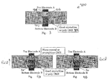
- Figs. 1A and 1B are partial cross-sectional views of a memory cell during programming (Fig. 1A) and erasing (Fig. 1B) operations.
- the top and bottom electrodes are identical and the memory resistance material is uniform throughout. If the geometric structure of the device could be made perfectly symmetrical, the net resistance would remains constant, in a high-resistance state, when either a negative field (Fig. 1A) or a positive field (Fig. 1B) is applied. Note that the electric fields are defined with respect to the top electrode. That is, the fields are induced at the top electrode. In such circumstances, programming is not possible. Therefore, a geometrically symmetrical device structure, such as one in Figs. 1A and 1B, is not practical.
- the geometrically symmetric memory cell has a high current density near the electrodes (regions A and B), and a low current density in the center portion of the device, in the presence of an electric field.
- the resistivity of the CMR material near the top and bottom electrodes is changed.
- the memory cell can be programmed to be in the high-resistance state if the resistivity of the memory resistor material near the top electrode is increased, and the resistivity of memory resistor material near the bottom electrode is decreased.
- region A and region B are very close to the top and bottom electrode, respectively, and their thicknesses may be as thin as a 10 nanometers (nm), the above-described effect may be mistakenly classified as an interface effect.
- memory is not an interface property change, but is a bulk resistivity change.
- Figs. 2A and 2B are partial cross-sectional views of a memory cell, where the memory resistor has a cylindrical shape and is embedded in oxide or any suitable insulator.
- the field intensity is high near both top and bottom electrodes. Since the field direction near the top electrode is opposite that near the bottom electrode, the resistivity of the memory resistor material near the top electrode is increased while the resistivity of the memory resistor material near the bottom electrode is reduced. As a result, the memory resistance is programmed to the high-resistance state regardless of whether a positive or negative pulse is applied to the top electrode. Again, a geometrically symmetrical structure is not suitable for resistor memory cell.
- Fig. 3 is a partial cross-section view of the present invention asymmetric crystalline structure memory cell.
- the present invention describes a memory cell that may be geometrically symmetrical in the sense that memory film is not dependent upon asymmetrical geometric device features to insure proper memory (resistance change) operation. Alternately stated, the film relies upon physically asymmetric features in the structure of the material to insure reliable memory properties.
- the cell 400 comprises a bottom electrode 402 and an EPVR material first layer 404 having a polycrystalline structure overlying the bottom electrode 402.
- An EPVR second layer 406 is adjacent the first layer 404, having either a nano-crystalline or amorphous structure.
- the second layer 406 may overlie the first layer 404.
- the first layer 404 may overlie the second layer 406.
- a top electrode 408 overlies the EPVR first and second layers 404/406.
- the cell 400 may be embedded in an oxide or other electrically insulating material 410.
- the EPVR first and second layers 404/406 are a material such as CMR, HTSC, or perovskite metal oxide materials.
- the bottom electrode 402 is a material such as Pt, TiN, TaN, TiAlN, TaAlN, Ag, Au, or Ir.
- the top electrode 408 can be Pt, TiN, TaN, TiAlN, TaAIN, Ag, Au, or Ir.
- a nano-crystalline structure is understood to mean a polycrystalline structure where the average grain size is in the nanometer range, smaller than a nanometer, or has a poorer crystalline structure than the polycrystalline structure of layer 404.
- the EPVR first layer 404 and the EPVR second layer 406 have a selectable resistance responsive to a pulsed electric field. That is, the overall or composite resistance is selectable.
- the EPVR first layer 404 has a selectable resistance responsive to a first pulsed electric field. In some aspects, the EPVR first layer 404 has a resistance that is selectable within a range of 100 ohms to 10 megaohms (Mohms), in response to applying a negative first electric field in the range of 0.1 megavolts per centimeter (MV/cm) to 0.4 MV/cm. In other aspects, the EPVR first layer 404 has a resistance that is selectable within a range of 100 ohms to 1000 ohms, in response to applying a positive first electric field in the range of 0.1 megavolts per centimeter (MV/cm) to 0.4 MV/cm. As used herein, the field direction is defined from the perspective of the electrode in contact with the EPVR second layer 406. As shown in Fig. 4A, the negative field direction is from the bottom electrode towards the top electrode, when the EPVR second layer is in contact with the top electrode.
- the EPVR second layer 406 has a constant resistance responsive to the first pulsed electric field (either positive or negative). That is, the resistance of the EPVR second layer 406 does not change in response to the first electric field. Typically, the EPVR second layer 406 has a resistance that changes by less than a factor of 2, in response to first pulsed electric field. In some aspects, the first electric field has a pulse width of less than 400 nanoseconds (ns). In other aspects, the first electric field has a pulse width in the range of 1 ns to 400 ns.
- the EPVR first layer 404 has a low-resistance region responsive to a second pulsed electric field, where the second pulsed electric field has a longer pulse width than the first electric field. Note that the low-resistance region is formed regardless of whether the second electric field is positive or negative.
- the first EPVR layer 404 has a low-resistance region responsive to the second electric field having a pulse width of greater than 400 ns. In other aspects, the second electric field has a pulse width in the range of 400 ns to 10 microsecond ( ⁇ s). In some aspects, the first EPVR layer 404 has a low-resistance region responsive to a second electric field in the range of 0.05 MV/cm to 0.5 MV/cm.
- the second pulsed electric field creates low-resistance regions from the high-resistance regions. If the EPVR first layer 404 initially includes low-resistance regions, the regions remain low-resistance in response to the second pulsed electric field.
- the EPVR first and second layers 404/406 each have a resistance of less than 1000 ohms in response to the second pulsed electric field. Only a EPVR second layer 406 with a nano-crystalline structure changes resistance in response to the second pulsed electric field. When the EPVR second layer 406 has an amorphous structure, it maintains a constant resistance responsive to the second pulsed electric field. The concept of resistance remaining constant may be considered to be relative in some aspects of the invention. For example, when the EPVR second layer 406 has an amorphous structure, its resistance that changes by less than a factor of 2, in response to the second pulsed electric field.
- PCMO is a form of CMR material.
- the programming window can be from a nanosecond to approximately 400 ns.
- the programming memory window is in the range of 400 ns, to more than 10 ⁇ s.
- Amorphous CMR does not exhibit memory properties. Therefore, it is possible to fabricate a resistor that has a well-crystallized material at the bottom portion of the resistor, and an amorphous material at the upper portion of the resistor. In this case, the upper portion of the resistor does not respond to a narrow pulse programming (write) process.
- resistor random access memory (RRAM) memory resistors with amorphous material as the bottom portion of the resistor, and crystalline material at the upper portion of the resistor. In this case only the upper portion of the resistor exhibits memory properties. In place of amorphous material, nano-crystalline or poor polycrystalline material can be used. As long as the so-called polycrystalline portion of the resistor is a significantly better crystallite, the memory shall work.
- RRAM resistor random access memory
- the memory cell is easily be fabricated by depositing the lower portion of memory resistor CMR material at high temperature, and depositing the upper portion of CMR material at lower temperature.
- Figs. 4A and 4B illustrate the programming of the present invention memory cell to low-resistance and high-resistance states, respectively.
- Fig. 5 is a flowchart illustrating the present invention method for forming an asymmetric crystalline structure memory cell. Although the method is depicted as a sequence of numbered steps for clarity, no order should be inferred from the numbering unless explicitly stated. It should be understood that some of these steps may be skipped, performed in parallel, or performed without the requirement of maintaining a strict order of sequence.
- the method begins at Step 500.
- Step 502 forms a bottom electrode.
- Step 504 forms an electrical pulse various resistance (EPVR) first layer having a polycrystalline structure overlying the bottom electrode.
- Step 506 forms an EPVR second layer adjacent the first layer, having either a nano-crystalline or amorphous structure. In some aspects, the second layer overlies the first layer. Note however, that Step 504 may occur after Step 506 in alternate aspects of the method.
- the EPVR first and second layers formed in Steps 504 and 506 are a material such as CMR, HTSC, or perovskite metal oxide materials.
- Step 508 forms a top electrode overlying the EPVR first and second layers.
- the top electrode formed in Step 508 and the bottom electrode formed in Step 502 are a material such as Pt, TiN, TaN, TiAIN, TaAlN, Ag, Au, or Ir. Note that the top and bottom electrodes can be different materials.
- forming an EPVR first layer having a polycrystalline structure in Step 504 includes depositing the EPVR first layer with a metalorganic spin coat (MOD) process at a temperature of greater than 550 degrees C.
- the EPVR first layer is deposited with a MOD process at a temperature in the range between 550 and 700 degrees C.
- Step 505 (not shown), of heating the MOD deposited EPVR first layer to remove solvents.
- forming an EPVR second layer adjacent the first layer in Step 506 includes forming the second layer overlying the first layer at a temperature less than, or equal to the 550 degrees C.
- forming an EPVR first layer having a polycrystalline structure in Step 504 includes depositing the EPVR first layer with a physical vapor deposition (PVD) process at a temperature of greater than 400 degrees C.
- the deposition temperature is in the range between 400 and 700 degrees C.
- forming an EPVR second layer adjacent the first layer includes forming the second layer with a PVD deposition process at a temperature at least 30 degrees C lower than the first layer deposition temperature.
- Step 506 includes forming the second layer at a temperature less than, or equal to the deposition temperature of the first layer.
- Step 510 applies an electric field to the EPVR first and second layers.
- Step 512 selectively modifies the resistance of the EPVR first and second layers in response to the pulse width of the electric field. More specifically, when Step 510 applies a first voltage pulse to the EPVR first and second layers, selectively modifying the resistance of the EPVR first and second layers in response to the pulse width of the voltage pulse in Step 512 includes substeps. Step 512a modifies the resistance in the EPVR first layer in response to the first voltage pulse. Step 512b maintains the resistance in the EPVR second layer in response to the first voltage pulse. In some aspects, the EPVR second layer resistance is maintained within a factor of 2.
- Step 510 applies a negative first voltage pulse to the top electrode. Then, modifying the resistance of the EPVR first layer in response to the first voltage pulse includes creating a high-resistance region in the EPVR first layer in response to the negative first voltage pulse. In other aspects, applying a voltage pulse to the EPVR first and second layers includes applying a positive first voltage pulse to the top electrode. Then, modifying the resistance of the EPVR first layer in response to the first voltage pulse includes creating a low-resistance region in the EPVR first layer in response to the positive first voltage pulse.
- Some aspects of the method include a further step, Step 514, of applying a second voltage pulse, having a longer pulse width than the first voltage pulse, to the EPVR first and second layers. Then, selectively modifying the resistance of the EPVR first and second layers in response to the pulse width of the voltage pulse (Step 512) includes creating a low-resistance state in the EPVR first and second layers in response to the second voltage pulse.
- Step 506 a low-resistance state is created in the EPVR first layer in response to the second voltage pulse.
- Step 512 maintains the resistance state of the amorphous EPVR second layer in response to the second voltage pulse.
- applying a first voltage pulse to the EPVR first and second layers in Step 510 includes applying a first electric field with a pulse width of less than 400 nanoseconds (ns).
- the first electric field has a pulse width in the range of 1 ns to 400 ns.
- applying a second voltage pulse to the EPVR first and second layers in Step 514 includes applying a second electric field with a pulse width of greater than 400 ns.
- the second electric field has a pulse width in the range of 400 ns to 10 microsecond ( ⁇ s).
- applying the negative first voltage pulse in Step 510 includes applying a pulsed electric field in the range of 0.1 megavolts per centimeter (MV/cm) to 0.4 MV/cm. Then, modifying the resistance through the EPVR first layer in response to the first voltage pulse (Step 512a) includes modifying the resistance within a range of 100 ohms to 10 megaohms (Mohms) in response to the negative first voltage pulse. As above. the field direction is defined from the perspective of the electrode in contact with the EPVR second layer.
- applying the positive first voltage pulse in Step 510 includes applying a pulsed electric field in the range of 0.1 megavolts per centimeter (MV/cm) to 0.4 MV/cm. Then, modifying the resistance through the EPVR first layer in response to the first voltage pulse (Step 512a) includes modifying the resistance within a range of 100 ohms to 1000 ohms in response to the positive first voltage pulse.
- applying the second voltage pulse in Step 514 includes applying an electric field in the range of 0.05 MV/cm to 0.5 MV/cm. Then, creating a low resistance state in the EPVR first layer in response to the second voltage pulse (Step 512) includes creating a EPVR first layer resistance of less than 1000 ohms. When Step 506 forms an amorphous EPVR second layer, and the same second field is applied, Step 512 maintains a resistance in the EPVR second layer of less than 1000 ohms. In other aspects, the amorphous EPVR second layer resistance is maintained within a factor of 2.
Abstract
Description
Claims (46)
- A method for forming an asymmetric crystalline structure memory cell, the method comprisingforming a bottom electrode;forming an electrical pulse various resistance (EPVR) material first layer having a polycrystalline structure overlying the bottom electrode;forming an EPVR second layer adjacent the first layer having a structure selected from the group including nano-crystalline and amorphous; and,forming a top electrode overlying the EPVR first and second layers.
- The method of claim 1 wherein forming an EPVR first layer having a polycrystalline structure includes depositing the EPVR first layer with a metalorganic spin coat (MOD) process at a temperature of greater than 550 degrees C.
- The method of claim 2 wherein depositing the EPVR first layer at a temperature of greater than 550 degrees C includes depositing the EPVR first layer with a MOD process at a temperature in the range between 550 and 700 degrees C.
- The method of claim 1 wherein forming an EPVR second layer adjacent the first layer having a structure selected from the group including nano-crystalline and amorphous, includes forming the second layer at a temperature less than, or equal to the deposition temperature of the first layer.
- The method of claim 3 further comprising:wherein forming an EPVR second layer adjacent the first layer having a structure selected from the group including nano-crystalline and amorphous, includes forming the second layer overlying the first layer at a temperature less than, or equal to the 550 degrees C.heating the MOD deposited EPVR first layer to remove solvents; and,
- The method of claim 1 further comprising:applying a voltage pulse to the EPVR first and second layers; and,selectively modifying the resistance of the EPVR first and second layers in response to the width of the pulse.
- The method of claim 6 wherein applying a voltage pulse to the EPVR first and second layers includes applying a first voltage pulse; and,
wherein selectively modifying the resistance of the EPVR first and second layers in response to the pulse width of the voltage pulse includes:modifying the resistance in the EPVR first layer in response to the first voltage pulse; and,maintaining the resistance in the EPVR second layer. - The method of claim 7 wherein applying a voltage pulse to the EPVR first and second layers includes applying a negative first voltage pulse to the top electrode; and,
wherein modifying the resistance of the EPVR first layer in response to the first voltage pulse includes creating a high-resistance region in the EPVR first layer in response to the negative first voltage pulse. - The method of claim 7 wherein applying an voltage pulse to the EPVR first and second layers includes applying a positive first voltage pulse to the top electrode; and,
wherein modifying the resistance of the EPVR first layer in response to first voltage pulse includes creating a low-resistance region in the EPVR first layer in response to the positive first voltage pulse. - The method of claim 7 further comprising:wherein selectively modifying the resistance of the EPVR first and second layers in response to the pulse width of the voltage pulse includes creating a low-resistance state in the EPVR first and second layers in response to the second voltage pulse.applying a second voltage pulse, having a longer pulse width than the first voltage pulse, to the EPVR first and second layers; and,
- The method of claim 10 wherein selectively modifying the resistance of the EPVR first and second layers in response to the pulse width of the voltage pulse includes creating a low-resistance state in the EPVR first layer in response to the second voltage pulse.
- The method of claim 11 wherein forming a EPVR second layer adjacent the first layer having a structure selected from the group including nano-crystalline and amorphous includes forming an amorphous structure; and,
wherein selectively modifying the resistance of the EPVR first and second layers in response to the pulse width of the voltage pulse includes maintaining the resistance state of the amorphous EPVR second layer in response to the second voltage pulse. - The method of claim 7 wherein applying a first voltage pulse to the EPVR first and second layers includes applying a first electric field with a pulse width of less than 400 nanoseconds (ns).
- The method of claim 13 wherein applying the first electric field with a pulse width of less than 400 ns includes using a pulse width in the range of 1 ns to 400 ns.
- The method of claim 10 wherein applying a second voltage pulse to the EPVR first and second layers includes applying a second electric field with a pulse width of greater than 400 ns.
- The method of claim 15 wherein applying the second electric field with a pulse width of greater than 400 ns includes using a pulse width in the range of 400 ns to 10 microsecond (µs).
- The method of claim 8 wherein applying the negative first voltage pulse includes applying a pulsed electric field in the range of 0.1 megavolts per centimeter (MV/cm) to 0.4 MV/cm; and,
wherein modifying the resistance through the EPVR first layer in response to the first voltage pulse includes modifying the resistance within a range of 100 ohms to 10 megaohms (Mohms) in response to the negative first voltage pulse. - The method of claim 11 wherein applying the second voltage pulse includes applying an electric field in the range of 0.05 MV/cm to 0.5 MV/cm; and,
wherein creating a low resistance state in the EPVR first layer in response to the second voltage pulse includes creating a EPVR first layer resistance of less than 1000 ohms. - The method of claim 12 wherein applying the second voltage pulse includes applying an electric field in the range of 0.05 MV/cm to 0.5 MV/cm; and,
wherein maintaining the resistance in the EPVR second layer includes maintaining a resistance in the EPVR second layer of less than 1000 ohms. - The method of claim 7 wherein maintaining the resistance state of the EPVR second layer in response to the first voltage pulse includes maintaining the resistance within a factor of 2.
- The method of claim 12 wherein maintaining the resistance state of the amorphous EPVR second layer in response to the second voltage pulse includes maintaining the resistance within a factor of 2.
- The method of claim 1 wherein forming an EPVR first layer and EPVR second layer includes using a material selected from the group including colossal magnetoresistance (CMR), high temperature super conductor (HTSC), and perovskite metal oxide materials.
- The method of claim 1 wherein forming an EPVR first layer having a polycrystalline structure includes depositing the EPVR first layer with a physical vapor deposition (PVD) process at a temperature of greater than 400 degrees C.
- The method of claim 23 wherein depositing the EPVR first layer at a temperature of greater than 400 degrees C includes depositing the EPVR first layer with a PVD process at a temperature in the range between 400 and 700 degrees C.
- The method of claim 23 wherein forming an EPVR second layer adjacent the first layer having a structure selected from the group including nano-crystalline and amorphous, includes forming the second layer with a PVD deposition process at a temperature at least 30 degrees C lower than the first layer deposition temperature.
- The method of claim 1 wherein forming a bottom electrode includes forming the bottom electrode from a material selected from the group including Pt, TiN, TaN, TiAlN, TaAlN, Ag, Au, and Ir; and,
wherein forming a top electrode includes forming the top electrode from a material selected from the group including Pt, TiN, TaN, TiAlN, TaAlN, Ag, Au, and Ir. - The method of claim 7 wherein applying an voltage pulse to the EPVR first and second layers includes applying a positive first voltage pulse to the top electrode; and,
wherein modifying the resistance of the EPVR first layer in response to first voltage pulse includes creating a low-resistance region in the EPVR first layer in response to the positive first voltage pulse. - The method of claim 27 wherein applying the positive first voltage pulse includes applying a pulsed electric field in the range of 0.1 megavolts per centimeter (MV/cm) to 0.4 MV/cm; and,
wherein modifying the resistance through the EPVR first layer in response to the first voltage pulse includes modifying the resistance within a range of 100 ohms to 1000 ohms in response to the positive first voltage pulse. - An asymmetric crystalline structure memory cell, the cell comprising:a bottom electrode;an electrical pulse various resistance (EPVR) material first layer having a polycrystalline structure overlying the bottom electrode;an EPVR second layer adjacent the first layer, having a structure selected from the group including nano-crystalline and amorphous; and,a top electrode overlying the EPVR first and second layers.
- The memory cell of claim 29 wherein the EPVR first and second layers have a selectable resistance responsive to a pulsed electric field.
- The memory cell of claim 30 wherein the EPVR first layer has a selectable resistance responsive to a first pulsed electric field.
- The memory cell of claim 31 wherein the EPVR second layer has a constant resistance responsive to the first pulsed electric field.
- The memory cell of claim 32 wherein the EPVR first and second layers have low-resistance regions responsive to a second pulsed electric field, having a longer pulse width than the first electric field.
- The memory cell of claim 33 wherein the EPVR second layer has an amorphous structure and maintains a constant resistance responsive to the second pulsed electric field.
- The memory cell of claim 34 wherein the EPVR first layer has a selectable resistance responsive to the first electric field having a pulse width of less than 400 nanoseconds (ns).
- The memory cell of claim 35 wherein the EPVR first layer has a selectable resistance responsive to the first electric field having a pulse width in the range of 1 ns to 400 ns.
- The memory cell of claim 33 wherein the first EPVR layer has a low-resistance region responsive to the second electric field having a pulse width of greater than 400 ns.
- The memory cell of claim 37 wherein the first EPVR layer has a low-resistance region responsive to the second electric field having a pulse width in the range of 400 ns to 10 microsecond (µs).
- The memory cell of claim 33 wherein the first EPVR layer has a low-resistance region responsive to a second electric field in the range of 0.05 MV/cm to 0.5 MV/cm.
- The memory cell of claim 31 wherein the EPVR first layer resistance is selectable within a range of 100 ohms to 10 megaohms (Mohms) in response to applying a negative first electric field in the range of 0.1 megavolts per centimeter (MV/cm) to 0.4 MV/cm.
- The memory cell of claim 32 wherein the EPVR second layer has a resistance that changes by less than a factor of 2, in response to a first pulsed electric field.
- The memory cell of claim 34 wherein the EPVR second layer has an amorphous structure with a resistance that changes by less than a factor of 2, in response to the second pulsed electric field.
- The memory cell of claim 29 wherein the EPVR first and second layers are a material selected from the group including colossal magnetoresistance (CMR), high temperature super conductor (HTSC), and perovskite metal oxide materials.
- The memory cell of claim 29 wherein the bottom electrode is a material selected from the group including Pt, TiN, TaN, TiAIN, TaAlN, Ag, Au, and Ir; and,
wherein the top electrode is a material selected from the group including Pt, TiN, TaN, TiAlN, TaAlN, Ag, Au, and Ir. - The memory cell of claim 33 wherein the EPVR first and second layers each have low-resistance regions with a resistance of less than 1000 ohms in response to the second pulsed electric field.
- The memory cell of claim 31 wherein the EPVR first layer resistance is selectable within a range of 100 ohms to 1000 ohms in response to applying a positive first electric field in the range of 0.1 megavolts per centimeter (MV/cm) to 0.4 MV/cm.
Applications Claiming Priority (2)
| Application Number | Priority Date | Filing Date | Title |
|---|---|---|---|
| US442749 | 1989-11-29 | ||
| US10/442,749 US6927120B2 (en) | 2003-05-21 | 2003-05-21 | Method for forming an asymmetric crystalline structure memory cell |
Publications (3)
| Publication Number | Publication Date |
|---|---|
| EP1511085A2 true EP1511085A2 (en) | 2005-03-02 |
| EP1511085A3 EP1511085A3 (en) | 2006-03-22 |
| EP1511085B1 EP1511085B1 (en) | 2011-01-26 |
Family
ID=33450276
Family Applications (1)
| Application Number | Title | Priority Date | Filing Date |
|---|---|---|---|
| EP04011964A Active EP1511085B1 (en) | 2003-05-21 | 2004-05-19 | Asymmetric crystalline structure memory cell |
Country Status (7)
| Country | Link |
|---|---|
| US (2) | US6927120B2 (en) |
| EP (1) | EP1511085B1 (en) |
| JP (1) | JP4784960B2 (en) |
| KR (1) | KR100731936B1 (en) |
| CN (1) | CN1574288A (en) |
| DE (1) | DE602004031182D1 (en) |
| TW (1) | TWI270206B (en) |
Families Citing this family (34)
| Publication number | Priority date | Publication date | Assignee | Title |
|---|---|---|---|---|
| US5651855A (en) | 1992-07-28 | 1997-07-29 | Micron Technology, Inc. | Method of making self aligned contacts to silicon substrates during the manufacture of integrated circuits |
| US7009235B2 (en) * | 2003-11-10 | 2006-03-07 | Unity Semiconductor Corporation | Conductive memory stack with non-uniform width |
| US7326979B2 (en) * | 2002-08-02 | 2008-02-05 | Unity Semiconductor Corporation | Resistive memory device with a treated interface |
| US7042035B2 (en) * | 2002-08-02 | 2006-05-09 | Unity Semiconductor Corporation | Memory array with high temperature wiring |
| US6965137B2 (en) * | 2002-08-02 | 2005-11-15 | Unity Semiconductor Corporation | Multi-layer conductive memory device |
| US7402456B2 (en) * | 2004-04-23 | 2008-07-22 | Sharp Laboratories Of America, Inc. | PCMO thin film with memory resistance properties |
| US7235407B2 (en) * | 2004-05-27 | 2007-06-26 | Sharp Laboratories Of America, Inc. | System and method for forming a bipolar switching PCMO film |
| US7029982B1 (en) * | 2004-10-21 | 2006-04-18 | Sharp Laboratories Of America, Inc. | Method of affecting RRAM characteristics by doping PCMO thin films |
| JP2008060091A (en) * | 2005-01-14 | 2008-03-13 | Matsushita Electric Ind Co Ltd | Resistance variable element |
| DE102005035445B4 (en) * | 2005-07-28 | 2007-09-27 | Qimonda Ag | Non-volatile, resistive memory cell based on metal oxide nanoparticles, as well as processes for their preparation and corresponding memory cell arrangement |
| KR100657966B1 (en) | 2005-08-11 | 2006-12-14 | 삼성전자주식회사 | Manufacturing method of memory device for stablizing reset current |
| TWI394300B (en) * | 2007-10-24 | 2013-04-21 | Advanced Optoelectronic Tech | Packaging structure of photoelectric device and fabricating method thereof |
| US8395199B2 (en) | 2006-03-25 | 2013-03-12 | 4D-S Pty Ltd. | Systems and methods for fabricating self-aligned memory cell |
| US7407858B2 (en) * | 2006-04-11 | 2008-08-05 | Sharp Laboratories Of America, Inc. | Resistance random access memory devices and method of fabrication |
| JP2008021750A (en) * | 2006-07-11 | 2008-01-31 | Matsushita Electric Ind Co Ltd | Resistance change element, method for manufacturing the same, and resistance change memory using the same element |
| US8454810B2 (en) | 2006-07-14 | 2013-06-04 | 4D-S Pty Ltd. | Dual hexagonal shaped plasma source |
| US7932548B2 (en) | 2006-07-14 | 2011-04-26 | 4D-S Pty Ltd. | Systems and methods for fabricating self-aligned memory cell |
| JP4526587B2 (en) | 2006-07-27 | 2010-08-18 | パナソニック株式会社 | Nonvolatile semiconductor memory device and manufacturing method thereof |
| JP4105760B2 (en) | 2006-08-25 | 2008-06-25 | 松下電器産業株式会社 | Storage element, memory device, and semiconductor integrated circuit |
| US8308915B2 (en) | 2006-09-14 | 2012-11-13 | 4D-S Pty Ltd. | Systems and methods for magnetron deposition |
| WO2008047711A1 (en) | 2006-10-16 | 2008-04-24 | Panasonic Corporation | Non-volatile storage element array, and its manufacturing method |
| US9236381B2 (en) | 2006-11-17 | 2016-01-12 | Panasonic Intellectual Property Management Co., Ltd. | Nonvolatile memory element, nonvolatile memory apparatus, nonvolatile semiconductor apparatus, and method of manufacturing nonvolatile memory element |
| JP4252110B2 (en) | 2007-03-29 | 2009-04-08 | パナソニック株式会社 | Nonvolatile memory device, nonvolatile memory element, and nonvolatile memory element array |
| JP4299882B2 (en) | 2007-05-18 | 2009-07-22 | パナソニック株式会社 | Nonvolatile memory element, manufacturing method thereof, and nonvolatile semiconductor device using the nonvolatile memory element |
| EP2063467B1 (en) | 2007-06-05 | 2011-05-04 | Panasonic Corporation | Nonvolatile storage element, its manufacturing method, and nonvolatile semiconductor device using the nonvolatile storage element |
| KR101060793B1 (en) * | 2007-10-15 | 2011-08-30 | 파나소닉 주식회사 | Nonvolatile Memory and Nonvolatile Semiconductor Device Using the Nonvolatile Memory |
| JP4469023B2 (en) | 2008-07-11 | 2010-05-26 | パナソニック株式会社 | Nonvolatile memory element, manufacturing method thereof, and nonvolatile semiconductor device using the nonvolatile memory element |
| JP4607257B2 (en) | 2008-12-04 | 2011-01-05 | パナソニック株式会社 | Nonvolatile memory element and nonvolatile memory device |
| WO2010082928A1 (en) * | 2009-01-15 | 2010-07-22 | Hewlett-Packard Development Company, L.P. | Silicon-based memristive device |
| JP4757360B2 (en) | 2009-02-02 | 2011-08-24 | パナソニック株式会社 | Nonvolatile memory element, nonvolatile memory device, nonvolatile semiconductor device, and method of manufacturing nonvolatile memory element |
| KR101094390B1 (en) * | 2009-04-13 | 2011-12-15 | 주식회사 하이닉스반도체 | Resistive memory device and method for manufacturing the same |
| US8227783B2 (en) * | 2009-07-13 | 2012-07-24 | Seagate Technology Llc | Non-volatile resistive sense memory with praseodymium calcium manganese oxide |
| US8901527B2 (en) | 2010-07-02 | 2014-12-02 | Nanya Technology Corp. | Resistive random access memory structure with tri-layer resistive stack |
| CN112002801B (en) * | 2020-07-20 | 2021-09-07 | 厦门半导体工业技术研发有限公司 | Semiconductor device and method for manufacturing semiconductor device |
Citations (3)
| Publication number | Priority date | Publication date | Assignee | Title |
|---|---|---|---|---|
| US4272562A (en) * | 1979-06-19 | 1981-06-09 | Harris Corporation | Method of fabricating amorphous memory devices of reduced first fire threshold voltage |
| WO2000015882A2 (en) * | 1998-08-25 | 2000-03-23 | University Of Houston | Method for switching the properties of perovskite materials |
| EP1335417A2 (en) * | 2002-02-07 | 2003-08-13 | Sharp Kabushiki Kaisha | Method for fabricating variable resistance device, method for fabricating non-volatile variable resistance memory device, and non-volatile variable resistance memory device |
Family Cites Families (8)
| Publication number | Priority date | Publication date | Assignee | Title |
|---|---|---|---|---|
| JPH04272562A (en) * | 1991-02-25 | 1992-09-29 | Toyota Motor Corp | Structure of arrangement of oil pump in automatic transmission |
| JP3989027B2 (en) * | 1994-07-12 | 2007-10-10 | テキサス インスツルメンツ インコーポレイテツド | Capacitor and manufacturing method thereof |
| JP3012785B2 (en) * | 1995-07-14 | 2000-02-28 | 松下電子工業株式会社 | Capacitive element |
| JP3030333B2 (en) * | 1997-03-14 | 2000-04-10 | 工業技術院長 | Switching device and memory device using current and electric field induced phase transition |
| AU1887000A (en) * | 1999-02-17 | 2000-09-04 | International Business Machines Corporation | Microelectronic device for storing information and method thereof |
| US6531371B2 (en) * | 2001-06-28 | 2003-03-11 | Sharp Laboratories Of America, Inc. | Electrically programmable resistance cross point memory |
| US7011978B2 (en) * | 2001-08-17 | 2006-03-14 | Micron Technology, Inc. | Methods of forming capacitor constructions comprising perovskite-type dielectric materials with different amount of crystallinity regions |
| US6534326B1 (en) * | 2002-03-13 | 2003-03-18 | Sharp Laboratories Of America, Inc. | Method of minimizing leakage current and improving breakdown voltage of polycrystalline memory thin films |
-
2003
- 2003-05-21 US US10/442,749 patent/US6927120B2/en not_active Expired - Lifetime
-
2004
- 2004-04-27 JP JP2004132264A patent/JP4784960B2/en not_active Expired - Fee Related
- 2004-05-19 EP EP04011964A patent/EP1511085B1/en active Active
- 2004-05-19 DE DE602004031182T patent/DE602004031182D1/en active Active
- 2004-05-20 KR KR1020040036089A patent/KR100731936B1/en active IP Right Grant
- 2004-05-20 TW TW093114327A patent/TWI270206B/en active
- 2004-05-21 CN CNA2004100457140A patent/CN1574288A/en active Pending
-
2005
- 2005-05-16 US US11/130,983 patent/US7214583B2/en not_active Expired - Lifetime
Patent Citations (3)
| Publication number | Priority date | Publication date | Assignee | Title |
|---|---|---|---|---|
| US4272562A (en) * | 1979-06-19 | 1981-06-09 | Harris Corporation | Method of fabricating amorphous memory devices of reduced first fire threshold voltage |
| WO2000015882A2 (en) * | 1998-08-25 | 2000-03-23 | University Of Houston | Method for switching the properties of perovskite materials |
| EP1335417A2 (en) * | 2002-02-07 | 2003-08-13 | Sharp Kabushiki Kaisha | Method for fabricating variable resistance device, method for fabricating non-volatile variable resistance memory device, and non-volatile variable resistance memory device |
Also Published As
| Publication number | Publication date |
|---|---|
| EP1511085A3 (en) | 2006-03-22 |
| US20050207265A1 (en) | 2005-09-22 |
| TW200518331A (en) | 2005-06-01 |
| US6927120B2 (en) | 2005-08-09 |
| KR20040101035A (en) | 2004-12-02 |
| JP2004349689A (en) | 2004-12-09 |
| TWI270206B (en) | 2007-01-01 |
| KR100731936B1 (en) | 2007-06-25 |
| EP1511085B1 (en) | 2011-01-26 |
| US7214583B2 (en) | 2007-05-08 |
| DE602004031182D1 (en) | 2011-03-10 |
| JP4784960B2 (en) | 2011-10-05 |
| CN1574288A (en) | 2005-02-02 |
| US20040235247A1 (en) | 2004-11-25 |
Similar Documents
| Publication | Publication Date | Title |
|---|---|---|
| US7214583B2 (en) | Memory cell with an asymmetric crystalline structure | |
| US6972238B2 (en) | Oxygen content system and method for controlling memory resistance properties | |
| US7029924B2 (en) | Buffered-layer memory cell | |
| EP1542276B1 (en) | Memory cell with a layer having colossal magnetoresistance and an asymmetric area | |
| US7998804B2 (en) | Nonvolatile memory device including nano dot and method of fabricating the same | |
| KR101456766B1 (en) | Resistive memory and methods of processing resistive memory | |
| US7974117B2 (en) | Non-volatile memory cell with programmable unipolar switching element | |
| US20080062740A1 (en) | Methods of programming a resistive memory device | |
| US8274067B2 (en) | Memory devices and methods of manufacturing the same | |
| JP2007134724A (en) | Nonvolatile memory element and its manufacturing method | |
| JP2010123989A (en) | Asymmetric memory cell | |
| EP2535898A1 (en) | Multi-bit memory elements, memory devices including the same, and methods of manufacturing the same | |
| WO2016099525A1 (en) | Negative differential resistance (ndr) device based on fast diffusive metal atoms | |
| WO2015038158A1 (en) | Switching resistance memory devices with interfacial channels |
Legal Events
| Date | Code | Title | Description |
|---|---|---|---|
| PUAI | Public reference made under article 153(3) epc to a published international application that has entered the european phase |
Free format text: ORIGINAL CODE: 0009012 |
|
| AK | Designated contracting states |
Kind code of ref document: A2 Designated state(s): AT BE BG CH CY CZ DE DK EE ES FI FR GB GR HU IE IT LI LU MC NL PL PT RO SE SI SK TR |
|
| AX | Request for extension of the european patent |
Extension state: AL HR LT LV MK |
|
| PUAL | Search report despatched |
Free format text: ORIGINAL CODE: 0009013 |
|
| AK | Designated contracting states |
Kind code of ref document: A3 Designated state(s): AT BE BG CH CY CZ DE DK EE ES FI FR GB GR HU IE IT LI LU MC NL PL PT RO SE SI SK TR |
|
| AX | Request for extension of the european patent |
Extension state: AL HR LT LV MK |
|
| RIC1 | Information provided on ipc code assigned before grant |
Ipc: H01L 45/00 20060101AFI20060201BHEP |
|
| 17P | Request for examination filed |
Effective date: 20060908 |
|
| AKX | Designation fees paid |
Designated state(s): DE FR GB IT |
|
| 17Q | First examination report despatched |
Effective date: 20061102 |
|
| GRAP | Despatch of communication of intention to grant a patent |
Free format text: ORIGINAL CODE: EPIDOSNIGR1 |
|
| RIC1 | Information provided on ipc code assigned before grant |
Ipc: H01L 45/00 20060101AFI20100706BHEP |
|
| GRAS | Grant fee paid |
Free format text: ORIGINAL CODE: EPIDOSNIGR3 |
|
| GRAA | (expected) grant |
Free format text: ORIGINAL CODE: 0009210 |
|
| AK | Designated contracting states |
Kind code of ref document: B1 Designated state(s): DE FR GB IT |
|
| REG | Reference to a national code |
Ref country code: GB Ref legal event code: FG4D |
|
| REF | Corresponds to: |
Ref document number: 602004031182 Country of ref document: DE Date of ref document: 20110310 Kind code of ref document: P |
|
| REG | Reference to a national code |
Ref country code: DE Ref legal event code: R096 Ref document number: 602004031182 Country of ref document: DE Effective date: 20110310 |
|
| PLBE | No opposition filed within time limit |
Free format text: ORIGINAL CODE: 0009261 |
|
| STAA | Information on the status of an ep patent application or granted ep patent |
Free format text: STATUS: NO OPPOSITION FILED WITHIN TIME LIMIT |
|
| 26N | No opposition filed |
Effective date: 20111027 |
|
| GBPC | Gb: european patent ceased through non-payment of renewal fee |
Effective date: 20110519 |
|
| REG | Reference to a national code |
Ref country code: FR Ref legal event code: ST Effective date: 20120131 |
|
| REG | Reference to a national code |
Ref country code: DE Ref legal event code: R097 Ref document number: 602004031182 Country of ref document: DE Effective date: 20111027 |
|
| PG25 | Lapsed in a contracting state [announced via postgrant information from national office to epo] |
Ref country code: FR Free format text: LAPSE BECAUSE OF NON-PAYMENT OF DUE FEES Effective date: 20110531 |
|
| PG25 | Lapsed in a contracting state [announced via postgrant information from national office to epo] |
Ref country code: IT Free format text: LAPSE BECAUSE OF FAILURE TO SUBMIT A TRANSLATION OF THE DESCRIPTION OR TO PAY THE FEE WITHIN THE PRESCRIBED TIME-LIMIT Effective date: 20110126 |
|
| PG25 | Lapsed in a contracting state [announced via postgrant information from national office to epo] |
Ref country code: GB Free format text: LAPSE BECAUSE OF NON-PAYMENT OF DUE FEES Effective date: 20110519 |
|
| REG | Reference to a national code |
Ref country code: DE Ref legal event code: R082 Ref document number: 602004031182 Country of ref document: DE Representative=s name: MUELLER - HOFFMANN & PARTNER PATENTANWAELTE, DE |
|
| REG | Reference to a national code |
Ref country code: DE Ref legal event code: R082 Ref document number: 602004031182 Country of ref document: DE Representative=s name: MUELLER HOFFMANN & PARTNER PATENTANWAELTE MBB, DE Effective date: 20130612 Ref country code: DE Ref legal event code: R081 Ref document number: 602004031182 Country of ref document: DE Owner name: SAMSUNG ELECTRONICS CO., LTD., SUWON-SI, KR Free format text: FORMER OWNER: SHARP K.K., OSAKA, JP Effective date: 20130612 Ref country code: DE Ref legal event code: R081 Ref document number: 602004031182 Country of ref document: DE Owner name: INTELLECTUAL PROPERTIES I KFT., HU Free format text: FORMER OWNER: SHARP K.K., OSAKA, JP Effective date: 20130612 Ref country code: DE Ref legal event code: R082 Ref document number: 602004031182 Country of ref document: DE Representative=s name: MUELLER - HOFFMANN & PARTNER PATENTANWAELTE, DE Effective date: 20130612 |
|
| REG | Reference to a national code |
Ref country code: DE Ref legal event code: R082 Ref document number: 602004031182 Country of ref document: DE Representative=s name: MUELLER HOFFMANN & PARTNER PATENTANWAELTE MBB, DE Ref country code: DE Ref legal event code: R081 Ref document number: 602004031182 Country of ref document: DE Owner name: SAMSUNG ELECTRONICS CO., LTD., SUWON-SI, KR Free format text: FORMER OWNER: INTELLECTUAL PROPERTIES I KFT., BUDAPEST, HU |
|
| REG | Reference to a national code |
Ref country code: DE Ref legal event code: R079 Ref document number: 602004031182 Country of ref document: DE Free format text: PREVIOUS MAIN CLASS: H01L0045000000 Ipc: H10N0070000000 |
|
| P01 | Opt-out of the competence of the unified patent court (upc) registered |
Effective date: 20230524 |
|
| PGFP | Annual fee paid to national office [announced via postgrant information from national office to epo] |
Ref country code: DE Payment date: 20230321 Year of fee payment: 20 |