EP1510863A2 - Mask and method of fabricating the same, and method of machining material - Google Patents
Mask and method of fabricating the same, and method of machining material Download PDFInfo
- Publication number
- EP1510863A2 EP1510863A2 EP04020159A EP04020159A EP1510863A2 EP 1510863 A2 EP1510863 A2 EP 1510863A2 EP 04020159 A EP04020159 A EP 04020159A EP 04020159 A EP04020159 A EP 04020159A EP 1510863 A2 EP1510863 A2 EP 1510863A2
- Authority
- EP
- European Patent Office
- Prior art keywords
- material layer
- soft material
- mask
- forming
- mask pattern
- Prior art date
- Legal status (The legal status is an assumption and is not a legal conclusion. Google has not performed a legal analysis and makes no representation as to the accuracy of the status listed.)
- Withdrawn
Links
- 239000000463 material Substances 0.000 title claims abstract description 263
- 238000000034 method Methods 0.000 title claims abstract description 128
- 238000003754 machining Methods 0.000 title claims abstract description 72
- 238000004519 manufacturing process Methods 0.000 title claims abstract description 25
- 239000007779 soft material Substances 0.000 claims abstract description 218
- 229910052751 metal Inorganic materials 0.000 claims description 80
- 239000002184 metal Substances 0.000 claims description 80
- 238000005488 sandblasting Methods 0.000 claims description 52
- 238000005530 etching Methods 0.000 claims description 24
- 238000005096 rolling process Methods 0.000 claims description 23
- 206010034972 Photosensitivity reaction Diseases 0.000 claims description 15
- 239000007788 liquid Substances 0.000 claims description 15
- 230000036211 photosensitivity Effects 0.000 claims description 15
- 239000013013 elastic material Substances 0.000 claims description 14
- 239000010410 layer Substances 0.000 description 242
- 230000003287 optical effect Effects 0.000 description 19
- 239000006061 abrasive grain Substances 0.000 description 17
- 238000010586 diagram Methods 0.000 description 14
- 239000000853 adhesive Substances 0.000 description 9
- 230000001070 adhesive effect Effects 0.000 description 9
- 230000018109 developmental process Effects 0.000 description 9
- 238000005422 blasting Methods 0.000 description 8
- 230000000694 effects Effects 0.000 description 8
- 230000009477 glass transition Effects 0.000 description 8
- 229920005989 resin Polymers 0.000 description 8
- 239000011347 resin Substances 0.000 description 8
- 238000001723 curing Methods 0.000 description 7
- 238000001039 wet etching Methods 0.000 description 7
- PXHVJJICTQNCMI-UHFFFAOYSA-N Nickel Chemical compound [Ni] PXHVJJICTQNCMI-UHFFFAOYSA-N 0.000 description 6
- 238000010304 firing Methods 0.000 description 6
- 230000003014 reinforcing effect Effects 0.000 description 6
- BQCADISMDOOEFD-UHFFFAOYSA-N Silver Chemical compound [Ag] BQCADISMDOOEFD-UHFFFAOYSA-N 0.000 description 5
- 239000010949 copper Substances 0.000 description 5
- 238000005553 drilling Methods 0.000 description 5
- 238000001312 dry etching Methods 0.000 description 5
- 230000035939 shock Effects 0.000 description 5
- 229910052709 silver Inorganic materials 0.000 description 5
- 239000004332 silver Substances 0.000 description 5
- 239000010935 stainless steel Substances 0.000 description 5
- 229910001220 stainless steel Inorganic materials 0.000 description 5
- XUIMIQQOPSSXEZ-UHFFFAOYSA-N Silicon Chemical compound [Si] XUIMIQQOPSSXEZ-UHFFFAOYSA-N 0.000 description 4
- PNEYBMLMFCGWSK-UHFFFAOYSA-N aluminium oxide Inorganic materials [O-2].[O-2].[O-2].[Al+3].[Al+3] PNEYBMLMFCGWSK-UHFFFAOYSA-N 0.000 description 4
- 239000000919 ceramic Substances 0.000 description 4
- 239000011521 glass Substances 0.000 description 4
- 230000007261 regionalization Effects 0.000 description 4
- 229910052710 silicon Inorganic materials 0.000 description 4
- 239000010703 silicon Substances 0.000 description 4
- 229910000679 solder Inorganic materials 0.000 description 4
- RYGMFSIKBFXOCR-UHFFFAOYSA-N Copper Chemical compound [Cu] RYGMFSIKBFXOCR-UHFFFAOYSA-N 0.000 description 3
- 239000004593 Epoxy Substances 0.000 description 3
- 239000012790 adhesive layer Substances 0.000 description 3
- 230000008859 change Effects 0.000 description 3
- 229910052802 copper Inorganic materials 0.000 description 3
- 239000003822 epoxy resin Substances 0.000 description 3
- 238000005459 micromachining Methods 0.000 description 3
- 229920000647 polyepoxide Polymers 0.000 description 3
- 238000003825 pressing Methods 0.000 description 3
- 239000000523 sample Substances 0.000 description 3
- 239000000126 substance Substances 0.000 description 3
- JOYRKODLDBILNP-UHFFFAOYSA-N Ethyl urethane Chemical compound CCOC(N)=O JOYRKODLDBILNP-UHFFFAOYSA-N 0.000 description 2
- XEEYBQQBJWHFJM-UHFFFAOYSA-N Iron Chemical compound [Fe] XEEYBQQBJWHFJM-UHFFFAOYSA-N 0.000 description 2
- ZOKXTWBITQBERF-UHFFFAOYSA-N Molybdenum Chemical compound [Mo] ZOKXTWBITQBERF-UHFFFAOYSA-N 0.000 description 2
- RTAQQCXQSZGOHL-UHFFFAOYSA-N Titanium Chemical compound [Ti] RTAQQCXQSZGOHL-UHFFFAOYSA-N 0.000 description 2
- MCMNRKCIXSYSNV-UHFFFAOYSA-N Zirconium dioxide Chemical compound O=[Zr]=O MCMNRKCIXSYSNV-UHFFFAOYSA-N 0.000 description 2
- 229910045601 alloy Inorganic materials 0.000 description 2
- 239000000956 alloy Substances 0.000 description 2
- 229910002113 barium titanate Inorganic materials 0.000 description 2
- 230000015572 biosynthetic process Effects 0.000 description 2
- 239000002131 composite material Substances 0.000 description 2
- 238000009792 diffusion process Methods 0.000 description 2
- 238000009826 distribution Methods 0.000 description 2
- 238000005516 engineering process Methods 0.000 description 2
- 239000011159 matrix material Substances 0.000 description 2
- 229910052750 molybdenum Inorganic materials 0.000 description 2
- 239000011733 molybdenum Substances 0.000 description 2
- 229910052759 nickel Inorganic materials 0.000 description 2
- 230000002093 peripheral effect Effects 0.000 description 2
- 239000011295 pitch Substances 0.000 description 2
- 238000001020 plasma etching Methods 0.000 description 2
- 238000005498 polishing Methods 0.000 description 2
- 239000011241 protective layer Substances 0.000 description 2
- 239000004065 semiconductor Substances 0.000 description 2
- 238000005507 spraying Methods 0.000 description 2
- 238000004544 sputter deposition Methods 0.000 description 2
- 229920002803 thermoplastic polyurethane Polymers 0.000 description 2
- 230000008719 thickening Effects 0.000 description 2
- WFKWXMTUELFFGS-UHFFFAOYSA-N tungsten Chemical compound [W] WFKWXMTUELFFGS-UHFFFAOYSA-N 0.000 description 2
- 229910052721 tungsten Inorganic materials 0.000 description 2
- 239000010937 tungsten Substances 0.000 description 2
- UONOETXJSWQNOL-UHFFFAOYSA-N tungsten carbide Chemical compound [W+]#[C-] UONOETXJSWQNOL-UHFFFAOYSA-N 0.000 description 2
- 229910002353 SrRuO3 Inorganic materials 0.000 description 1
- GWEVSGVZZGPLCZ-UHFFFAOYSA-N Titan oxide Chemical compound O=[Ti]=O GWEVSGVZZGPLCZ-UHFFFAOYSA-N 0.000 description 1
- 238000003848 UV Light-Curing Methods 0.000 description 1
- XLOMVQKBTHCTTD-UHFFFAOYSA-N Zinc monoxide Chemical compound [Zn]=O XLOMVQKBTHCTTD-UHFFFAOYSA-N 0.000 description 1
- 229910007667 ZnOx Inorganic materials 0.000 description 1
- JFWLFXVBLPDVDZ-UHFFFAOYSA-N [Ru]=O.[Sr] Chemical compound [Ru]=O.[Sr] JFWLFXVBLPDVDZ-UHFFFAOYSA-N 0.000 description 1
- 230000001464 adherent effect Effects 0.000 description 1
- 239000012670 alkaline solution Substances 0.000 description 1
- 229910052782 aluminium Inorganic materials 0.000 description 1
- XAGFODPZIPBFFR-UHFFFAOYSA-N aluminium Chemical compound [Al] XAGFODPZIPBFFR-UHFFFAOYSA-N 0.000 description 1
- 238000004458 analytical method Methods 0.000 description 1
- 230000003466 anti-cipated effect Effects 0.000 description 1
- 238000003491 array Methods 0.000 description 1
- JRPBQTZRNDNNOP-UHFFFAOYSA-N barium titanate Chemical compound [Ba+2].[Ba+2].[O-][Ti]([O-])([O-])[O-] JRPBQTZRNDNNOP-UHFFFAOYSA-N 0.000 description 1
- 230000004888 barrier function Effects 0.000 description 1
- 230000008901 benefit Effects 0.000 description 1
- 230000005540 biological transmission Effects 0.000 description 1
- 238000006243 chemical reaction Methods 0.000 description 1
- 229910052593 corundum Inorganic materials 0.000 description 1
- 238000000354 decomposition reaction Methods 0.000 description 1
- 238000007599 discharging Methods 0.000 description 1
- 229920001971 elastomer Polymers 0.000 description 1
- 230000005684 electric field Effects 0.000 description 1
- 238000005243 fluidization Methods 0.000 description 1
- 230000005484 gravity Effects 0.000 description 1
- 229910052736 halogen Inorganic materials 0.000 description 1
- 150000002367 halogens Chemical class 0.000 description 1
- 230000020169 heat generation Effects 0.000 description 1
- 238000010438 heat treatment Methods 0.000 description 1
- 230000006872 improvement Effects 0.000 description 1
- 229910052738 indium Inorganic materials 0.000 description 1
- APFVFJFRJDLVQX-UHFFFAOYSA-N indium atom Chemical compound [In] APFVFJFRJDLVQX-UHFFFAOYSA-N 0.000 description 1
- 229910052746 lanthanum Inorganic materials 0.000 description 1
- FZLIPJUXYLNCLC-UHFFFAOYSA-N lanthanum atom Chemical compound [La] FZLIPJUXYLNCLC-UHFFFAOYSA-N 0.000 description 1
- 230000000873 masking effect Effects 0.000 description 1
- 239000007769 metal material Substances 0.000 description 1
- 239000000203 mixture Substances 0.000 description 1
- 150000004767 nitrides Chemical class 0.000 description 1
- 230000000737 periodic effect Effects 0.000 description 1
- 230000010287 polarization Effects 0.000 description 1
- 230000008569 process Effects 0.000 description 1
- 230000009467 reduction Effects 0.000 description 1
- 230000002787 reinforcement Effects 0.000 description 1
- HBMJWWWQQXIZIP-UHFFFAOYSA-N silicon carbide Chemical compound [Si+]#[C-] HBMJWWWQQXIZIP-UHFFFAOYSA-N 0.000 description 1
- 239000002356 single layer Substances 0.000 description 1
- 239000007787 solid Substances 0.000 description 1
- 239000007921 spray Substances 0.000 description 1
- 239000000758 substrate Substances 0.000 description 1
- XOLBLPGZBRYERU-UHFFFAOYSA-N tin dioxide Chemical compound O=[Sn]=O XOLBLPGZBRYERU-UHFFFAOYSA-N 0.000 description 1
- 229910001887 tin oxide Inorganic materials 0.000 description 1
- 229910001845 yogo sapphire Inorganic materials 0.000 description 1
Images






Classifications
-
- B—PERFORMING OPERATIONS; TRANSPORTING
- B24—GRINDING; POLISHING
- B24C—ABRASIVE OR RELATED BLASTING WITH PARTICULATE MATERIAL
- B24C1/00—Methods for use of abrasive blasting for producing particular effects; Use of auxiliary equipment in connection with such methods
- B24C1/04—Methods for use of abrasive blasting for producing particular effects; Use of auxiliary equipment in connection with such methods for treating only selected parts of a surface, e.g. for carving stone or glass
-
- G—PHYSICS
- G03—PHOTOGRAPHY; CINEMATOGRAPHY; ANALOGOUS TECHNIQUES USING WAVES OTHER THAN OPTICAL WAVES; ELECTROGRAPHY; HOLOGRAPHY
- G03F—PHOTOMECHANICAL PRODUCTION OF TEXTURED OR PATTERNED SURFACES, e.g. FOR PRINTING, FOR PROCESSING OF SEMICONDUCTOR DEVICES; MATERIALS THEREFOR; ORIGINALS THEREFOR; APPARATUS SPECIALLY ADAPTED THEREFOR
- G03F7/00—Photomechanical, e.g. photolithographic, production of textured or patterned surfaces, e.g. printing surfaces; Materials therefor, e.g. comprising photoresists; Apparatus specially adapted therefor
- G03F7/0015—Production of aperture devices, microporous systems or stamps
Definitions
- the present invention relates to a mask to be used when machining a material and a method of fabricating the mask, and further relates to a method of machining a material.
- the sandblasting method is a machining method of performing drilling and polishing a workpiece by blasting a polishing material (abrasive grain) at high pressure (for example, 0.3MPa to 0.4MPa) from a nozzle to spray the material on the workpiece.
- a polishing material abrasive grain
- high pressure for example, 0.3MPa to 0.4MPa
- a nozzle having a diameter about 0.5mm to 5mm is generally used, and, further by using a mask, a micropattern can be formed on the hard and brittle material.
- Such sandblasting method is used in the fields such as the manufacture of a plasma display panel, the manufacture of an ultrasonic transducer array, and MEMS (micro electromechanical system) related devices.
- the plasma etching method as one of the dry etching methods is a technique for etching a workpiece by making a reactive gas into a plasma state under low vacuum pressure, and mainly used for micromachining a semiconductor.
- a member having elasticity such as a dry-film resist is used as a mask.
- the reason is as follows. Since not only the target of machining but also the mask is damaged by the sprayed abrasive grain, it is necessary to absorb the shock by the abrasive grain. Further, in order to endure the reduction of the mask thickness, the mask is made to have a certain degree of thickness.
- abrasive grain is blasted for a long time.
- the longer the blasting time of abrasive grain the greater the damage to the mask becomes.
- the edge portion in the mask peripheral part is damaged greatly, the mask peripheral part recedes and the mask shape cannot be maintained.
- the formed pattern becomes tapered, and thus, there has been a problem that formation of a precise pattern with a high aspect ratio (drilling depth: pattern width) is difficult by the sandblasting method.
- a hard member such as a metal is used as a mask.
- the shock by the abrasive grain cannot be absorbed, and the durability of the mask becomes degraded instead.
- the thickness of the mask is made thicker. However, if the mask becomes thicker, the capability to reliably shield the target of machining from abrasive grain is degraded, and therefore, the accuracy of the pattern formation becomes lower.
- JP-A-5-205636 discloses in Fig. 3 ametal mask formed by providing an adhesive layer 12 on the back side of ametal thin plate 11 and a protective layer 13 on the front side thereof.
- the adhesive layer 12 brings the metal mask into close contact with the upper surface of a barrier 2 (Fig. 1 of the first document) and absorbs the rebound force of an abrasive at the time of sandblasting treatment.
- the protective layer 13 absorbs the shock of the abrasive at the time of sandblasting treatment and prevents the metal thin plate 11, especially its edge portion from wear, heat generation, and deformation. Further, the first document also discloses in Fig. 4 a metal mask having greater effect of absorbing the rebound force of an abrasive at the time of sandblasting treatment by further providing a cushion layer 14 consisting of a dry film between the metal thin plate 11 and the adhesive layer 12 in the above-mentioned metal mask.
- a composite mask in combination of a soft material and a hard material, the durability of the mask can be improved.
- such composite mask is for forming a "hollowing-out pattern" to be used when fabricating a fluorescent material pattern. That is, there is a problem that amask for forming an isolatedpattern, which is a reversal pattern of the "hollowing-out pattern", cannot be fabricated by the methods disclosed in the above-mentioned documents.
- An object of the present invention is to provide a mask which can endure the use for a long time and which can be used for forming an isolated pattern with a high aspect ratio.
- a fabricating method of a mask according to a first aspect of the present invention includes the steps of: (a) forming a soft material layer by disposing a soft material having positive photosensitivity and adhesion or adhesiveness on a material as a target of machining; (b) forming a hardmaterial layer by disposing an opaque hard material, in which a desired mask pattern has been formed in advance, on the soft material layer; and (c) forming the mask pattern in the soft material layer by performing exposure to light and development on the soft material layer by using the hard material layer as a photomask.
- a fabricating method of a mask according to a second aspect of the present invention includes the steps of: (a) forming a soft material layer by disposing a soft material having adhesion or adhesiveness on a material as a target of machining; (b) forming a hard material layer by disposing a hard material, in which a desired mask pattern has been formed in advance, on the soft material layer; and (c) forming the mask pattern in the soft material layer by etching the soft material layer by using the hard material layer as a mask.
- a fabricating method of a mask according to a third aspect of the present invention includes the steps of: (a) forming a soft material layer by disposing a soft material having negative photosensitivity and adhesion or adhesiveness on a material as a target of machining; (b) forming a desired mask pattern in the soft material layer by performing exposure to light and development on the soft material layer by using a photomask in which the mask pattern has been formed; and (c) disposing a hard material, in which the mask pattern has been formed in advance, on the soft material layer, in which the mask pattern has been formed, while aligning them with each other.
- a fabricating method of a mask according to a fourth aspect of the present invention includes the steps of: (a) forming a first soft material layer by disposing a soft material having adhesion or adhesiveness on a material as a target of machining; (b) forming a hard material layer by disposing a hard material on the first soft material layer; (c) forming a second soft material layer by disposing a soft material having photosensitivity and adhesion or adhesiveness on the hard material layer; (d) forming a desired mask pattern in the second soft material layer by performing exposure to light and development on the second soft material layer by using a photomask in which the mask pattern has been formed; and (e) forming the mask pattern in the soft material layer and the hard material layer by using the second soft material layer, in which the mask pattern has been formed, as a mask.
- a fabricating method of a mask according to a fifth aspect of the present invention includes the steps of: (a) forming a soft material layer by applying an elastic material in a liquid form or a paste form onto a material as a target of machining to form a mask pattern and curing the material; and (b) forming a hard material layer by applying a hard material in a liquid form or a paste form onto the soft material layer and curing the hard material.
- a mask according to one aspect of the present invention includes: a soft material layer formed on a material as a target of machining by employing a soft material, the soft material layer having an isolated mask pattern; and a hard material layer formed on the soft material layer by employing a hard material.
- a machining method of a material according to the first aspect of the present invention includes the steps of: (a) forming a soft material layer by disposing a soft material having positive photosensitivity and adhesion or adhesiveness on a material as a target of machining; (b) forming a hard material layer by disposing an opaque hard material, in which a desired mask pattern has been formed in advance, on the soft material layer; (c) forming the mask pattern in the soft material layer by performing exposure to light and development on the soft material layer by using the hard material layer as a photomask; and (d) removing a region of the material as the target of machining, on which the mask pattern is not formed, in accordance with a sandblasting method or an etching method.
- a machining method of a material according to the second aspect of the present invention includes the steps of: (a) forming a soft material layer by disposing a soft material having adhesion or adhesiveness on a material as a target of machining; (b) forming a hard material layer by disposing a hard material, in which a desired mask pattern has been formed in advance, on the soft material layer; (c) forming the mask pattern in the soft material layer by etching the soft material layer by using the hard material layer as a mask; and (d) removing a region of the material as the target of machining, on which the mask pattern is not formed, in accordance with a sandblasting method or an etching method.
- a machining method of a material includes the steps of: (a) forming a soft material layer by disposing a soft material having negative photosensitivity and adhesion or adhesiveness on a material as a target of machining; (b) forming a mask pattern in the soft material layer by performing exposure to light and development on the soft material layer by using a photomask in which a desired mask pattern has been formed; (c) disposing a hard material, in which the mask pattern has been formed in advance, on the soft material layer, in which the mask pattern has been formed, while aligning them with each other; and (d) removing a region of the material as the target of machining, on which the mask pattern is not formed, in accordance with a sandblasting method or an etching method.
- a machining method of a material includes the steps of: (a) forming a first soft material layer by disposing a soft material having adhesion or adhesiveness on a material as a target of machining; (b) forming a hard material layer by disposing a hard material on the first soft material layer; (c) forming a second soft material layer by disposing a soft material having photosensitivity and adhesion or adhesiveness on the hard material layer; (d) forming a desired mask pattern in the second sof t material layer by performing exposure to light and development on the second soft material layer by using a photomask in which the mask pattern has been formed; (e) forming the mask pattern in the first soft material layer and the hard material layer by using the second soft material layer, in which the mask pattern has been formed, as a mask; and (f) removing a region of the material as the target of machining; on which the mask pattern is not formed, in accordance with a sandblasting method or an etching method.
- a machining method of a material includes the steps of: (a) forming a soft material layer by applying an elastic material in a liquid form or a paste form to a material as a target of machining to form a mask pattern and curing the elastic material; (b) forming a hard material layer by applying a hard material in a liquid form or a paste form on the soft material layer and curing the hard material; and (c) removing a region of the material as the target of machining, on which the mask pattern is not formed, in accordance with a sandblasting method or an etching method by using the soft material layer and the hard material layer as a mask.
- durability of the mask to be used in the sandblasting method can be improved.
- the machining can be continued for a long time, which increases kinds of materials such as the hard and brittle material that can be machined in accordance with the sandblasting method.
- high aspect pattern formation with an aspect ratio exceeding 1:10 and a precise machining in which surface precision of the pattern edge portion is improved can be performed.
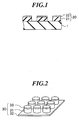
- Fig. 1 is a sectional view showing a mask according to the first embodiment of the present invention.
- the mask 20 is, for example, a mask to be used when sandblasting a hard and brittle material and, in the embodiment, formed on a PZT (Pb (lead) zirconate titanate) plate material 1 as a target of machining.
- PZT Pb (lead) zirconate titanate
- the mask 20 includes a soft material layer 21 and a hard material layer 22.
- the soft material layer 21 is formed by employing a soft material having elasticity.
- a material having a Young' s modulus from on the order of 1kgf/mm 2 to about 50kgf/mm 2 is desirably used, and specifically, a dry-film resist (DFR) , a general resist, urethane, an adhesive and so on can be used.
- DFR dry-film resist
- the hard material layer 22 is formed by employing a film of a hard material such as a metal or ceramics and protects the edge of the soft material layer 21.
- a material having a Young's modulus on the order of 10 4 kgf/mm 2 is desirably used.
- a metal such as SUS (stainless steel), copper (Cu), iron (Fe), nickel (Ni), tungsten (W), and molybdenum (Mo), or an alloy of them, PZT, PLZT (Pb (lead) lanthanum zirconate titanate), an oxide such as titanium oxide (TiO 2 ), zinc oxide (ZnO), tin oxide (SnO), alumina (Al 2 O 3 ), barium titanate (BaTiO 3 ), SRO (strontium ruthenium oxide: SrRuO 3 ), glass (SiO 2 ), and ITO (indium tine oxide), a nitride, etc. can be cited.
- SUS stainless steel
- Cu copper
- an oxide such as titanium
- Young's modulus of the hard material > Young's modulus of the soft material
- Young' s modulus of the hard material is a hundred times or more larger than Young's modulus of the soft material.
- a dry-film resist Young's modulus: about 0.5kgf /mm 2 to 2.5kgf /mm 2
- SUS 340 Young' s modulus: about 20000kgf/mm 2
- copper Young' s modulus : about 13868kgf/mm 2
- the hard material may be used as the hard material.
- the soft material layer 21 is protected at the time of blasting by providing the hard material layer 22 on the soft material layer 21, and thereby, the film thickness of the mask can be prevented from being thinner and the pattern can be prevented from being deformed due to receding of the edge. Further, by providing the soft material layer 21 having high elasticity, the soft material layer 21 serves as a cushion to absorb the shock applied to the hard material layer 22 at the time of blasting, and thereby, the durability of the hard material layer 22 can be made higher. Therefore, by using such mask, abrasive grain can be blasted for a long time while maintaining the mask pattern, and high-precision machining with high aspect can be performed.
- a fabricating method of the mask according to the first embodiment of the present invention and a machining method of a material using the mask will be described by referring to Fig. 2 to Fig. 5D.
- the case of manufacturing an ultrasonic transducer array in accordance with the sandblasting method is taken as an example.
- Fig. 2 is a perspective view showing an ultrasonic transducer array.
- This ultrasonic transducer array includes plural piezoelectric elements 31 arranged in a two-dimensional manner, a common electrode 32, and electrodes 33 formed on the respective piezoelectric elements 31.
- the piezoelectric elements 31 expand and contract by the piezoelectric effect to generate ultrasonic waves.
- the plural piezoelectric elements 31 are driven while providing time differences, and thereby, the ultrasonic waves generated from the respective piezoelectric elements are synthesized and an ultrasonic beam is transmitted.
- Fig. 3 is a flowchart showing a manufacturing method of an ultrasonic transducer array using the mask according to the embodiment
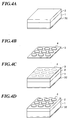
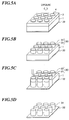
- Fig. 4A to Fig. 5D are diagrams for explanation of the manufacturing method of such an ultrasonic transducer array.
- the common electrode 32 is formed by attaching ametal plate on one surface of the PZT plate material 1 as the target of machining.
- the soft material layer 2 is formed on the PZT plate material 1.
- a positive type dry-film resist is used, and this is stacked on the PZT plate material 1.
- dry-film resists for sandblasting in thicknesses of, for example, 50 ⁇ m, 100 ⁇ m, 120 ⁇ m and so on are commercially available, and these can be used.
- a cushioning property is recognized.
- the resist about 50 ⁇ m is good.
- the film thickness is desirably selected so that the aspect ratio (drilling depth : pattern width) may be generally within 1/6.
- a hard material mask 4 having a desired pattern is formed on a thermal release sheet 3 by employing a hard material such as a metal in accordance with an etching method or the like.
- the thermal release sheet is a sheet-like adhesive member having an adhesive surface, and the sheet loses the adhesion of the adhesive surface and becomes releasable by being applied with heat.
- adhesive member for example, a product of NITTO DENKO CORPORATION, "RIVALPHA" can be used.
- the thermal release sheet 3 as shown in Fig. 4B, on which the hardmaterial mask 4 is formed is attached to the soft material layer (dry-film resist) 2 as shown in Fig. 4A.
- the hard material mask 4 is brought into contact with the soft material layer 2. Since the dry-film resist has adhesion, by attaching the thermal release sheet 3, on which the hard material mask 4 is formed, to the dry-film resist and applying pressure thereto, the hard material mask 4 adheres to the dry-film resist.
- steps S12 and S13 may be performed at the same time. That is, the dry-film resist and the thermal release sheet 3, on which the hard material mask 4 is formed, are overlapped on the PZT plate material 1 and applied with pressure by a roller or the like.
- the thermal release sheet 3 is overheated and released from the soft material layer 2 and the hard material mask 4. Thereby, as shown in Fig. 4D, the hard material mask 4 having an isolated pattern is formed on the soft material layer 2.
- step S15 as shown in Fig. 5A, the soft material layer (dry-film resist) 2, on which the hard material mask 4 is formed, is exposed by using, for example, ultraviolet light and, at step S16, development is performed by using, for example, a weakly alkaline solution.
- step S16 development is performed by using, for example, a weakly alkaline solution.
- sandblasting is performed by spraying abrasive grain onto the PZT plate material 1 on which the mask 20 has been formed.
- abrasive grain for example, alumina (AL 2 O 3 ), silicon carbide (SiC), zirconia (ZnOx), tungsten carbide (WC), etc. can be used.
- the mask 20 is removed in accordance with a method such as wet etching, for example.
- a method such as wet etching, for example.
- the electrodes 33 are formed on the upper surfaces of the respective PZT elements 31 in accordance with a method such as sputtering.
- the ultrasonic transducer array including plural ultrasonic transducers 30 is fabricated.
- the durability of the mask in sandblasting can be improved. Therefore, the mask form is maintained even blasted for a long time, and a micropattern with a high aspect ratio can be formed.
- abrasive grain having large specific gravity and high blasting performance as tungsten carbide
- machining by taking advantage of high blasting performance can be performed.
- the mask pattern is formed by forming the metal mask on the thermal release sheet and transferring it onto the soft material layer, not only the hollowing-out pattern but also the isolated pattern, which is the reversal pattern of the hollowing-out pattern, can be formed.
- the thermal release sheet is used when the hard material mask is formed, however, a member that can be released by a stimulus other than heat may be used.
- a UV release sheet that loses adhesion by being applied with ultraviolet light may be used.
- the common electrode is providedby attaching the metal plate to the PZT plate material , however, the common electrode may be provided by forming a metal film on the PZT plate material.
- the metal film may be formed on the PZT plate material first, or the metal film may be formed after the sandblasting on the PZT plate material is completed.
- a fabricating method of a mask according to the second embodiment will be described.
- the positive type photosensitive dry-film resist is used as the softmaterial layer 21, however, a negative type photosensitive dry-film resist may be used.
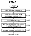
- Fig. 6 is a flowchart showing the fabricating method of a mask according to the second embodiment.
- Figs. 7A to 7D are diagrams for explanation of the fabricating method of the mask using a negative type photosensitive dry-film resist.
- a soft material layer 5 is formed on a PZT plate material 1 as a target of machining.
- a negative type photosensitive dry-film resist is used, and it is stacked on the PZT plate material 1.
- a hard material mask 4 made of a metal or the like is formed on a thermal release sheet 3 in accordance with an etching method or the like.
- a mask pattern is formed by performing exposure, development, etc. on the softmaterial layer (dry-film resist) by using a photomask 6.
- a photomask 6 As the photomask 6, a mask having the same pattern as the hard material mask 4 formed at step S22 is used. Thereby, as shown in Fig. 7D, a soft material layer 5a, in which the mask pattern is formed, is formed.
- the thermal release sheet 3, in which the hard material mask 4 has been formed at step S21, is attached onto the soft material layer 5a in which the mask pattern has been formed.
- the sheet is disposed while making alignment so that the position of the hard material mask 4 may match the position of the mask pattern of the soft material layer 5a.
- the thermal release sheet 3 is overheated and released from the hard material mask 4 and the soft material layer 5a. Thereby, as shown in Fig. 8B, the mask 20 including the soft material layer 21 and the hard material layer 22 is fabricated.
- a desired pattern is formed on the PZT plate material 1 by performing sandblasting by using the mask 20.
- the photosensitive dry-film resist is used as the soft material layer 21, however, the third embodiment is characterized in that a non-photosensitive member is used as the soft material layer 21.
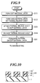
- Fig. 9 is a flowchart showing the fabricating method of the mask according to the embodiment.
- the thermal release sheet 3, on which the hard material mask 4 has been formed is attached onto the soft material layer 2 that has been formed on the PZT plate material 1, and the thermal release sheet 3 is overheated and released.
- the soft material layer 2 a non-photosensitive member such as an adhesive or the like may be used.
- a mask pattern is formed by removing the region of the soft material layer 2 on which the hard material mask 4 is not formed.
- a publicly known method such as dry etching, wet etching, sandblasting and so on can be used.
- the mask 20 including the soft material layer 21 and the hard material layer 22 is fabricated.
- a desired pattern is formed on the PZT plate material 1 by performing sandblasting by using the mask 20.
- Fig. 10 is a sectional view showing the mask according to the fourth embodiment.
- the mask 40 is a mask to be used at the time of sandblasting, and formed on a PZT plate material 1 as a target of machining.
- the mask 40 includes a first soft material layer 41, a hard material layer 42, and a second soft material layer 43.
- the first soft material layer 41 is formed by employing an adhesive or adherent material having flexibility and elasticity directly on the PZT plate material 1.
- the first soft material layer 41 serves as a cushion for absorbing a shock applied onto the hard material layer 42 at the time of sandblasting.
- This first soft material layer 41 may be either of photosensitive or non-photosensitive material.
- the hard material layer 42 is formed as a film of a hard material such as a metal or ceramics on the first soft material layer 41.
- the hard material layer 42 protects the soft material layer 41 at the time of blasting, and prevents the film thickness of the mask from being thinner and the pattern deformation due to receding of the edge.
- the second soft material layer 43 is formed by employing a soft material having photosensitivity such as a positive type or negative type dry-film resist.
- the second soft material layer 43 protects the hard material layer 42 and serves as a mask when a pattern is formed in the first soft material layer 41 and the hard material layer 42.
- the second soft material layer 43 may be a member having weak adhesion or adhesiveness.
- the second soft material layer 43 is easily damaged at the time of blasting.
- the film thickness of the second soft material layer 43 becomes thinner or its edge recedes, the pattern of the whole mask is maintained by the hard material layer 42 in the under layer thereof, and therefore, good masking performance can be maintained even when sandblasting is performed for a long time.
- the thickness of the soft material layer 41 is thick, as long as the resolution of the second soft material layer 43 is high, machining at a high aspect ratio can be performed.
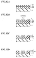
- FIG. 11 is a flowchart showing the fabricating method of the mask according to the fourth embodiment.
- Figs. 12A to 12D are diagrams for explanation of the fabricating method of the mask according to the fourth embodiment.
- a first soft material layer 41a, a hard material layer 42a, and a second soft material layer 43a are sequentially formed on a PZT plate material 1.
- step S42 as shown in Fig. 12B, the second soft material layer 43a is exposed to light by using a photomask 7 and further developed. Thereby, as shown in Fig. 12C, the second soft material layer 43, in which a mask pattern is formed, is obtained.
- etching is performed on the hard material layer 42a and the first soft material layer 41a.
- the etching method to be used at the time may be either dry etching or wet etching, and a publicly known etching method can be used. Further, the etching method may be changed between the hardmaterial layer 42a and the first soft material layer 41a, and a suitable etching method may be selected according to the material.
- the mask 40 including the first soft material layer 41, the hard material layer 42, and the second soft material layer 43 is fabricated. Furthermore, by performing sandblasting by using the mask 40, a desired pattern is formed on the PZT plate material 1.
- the pattern is formed in the under layer by using the second soft material layer as a mask, and therefore, the range of choice of the material usable for the under layer such as the first soft material layer can be broadened.
- the mask in which single layers of the first soft material layer 41, the hard material layer 42, and the second soft material layer 43 are stacked is fabricated, however, a mask having a periodic structure may be formed by further stacking these layers alternately. Especially, in the case of forming a pattern with a large aspect ratio, it is desired that the number of stacked layers is determined according to the drilling depth.
- Fig. 13 is a partially sectional perspective view showing the mask according to the fifth embodiment.
- an arrow indicates the rolling direction of a metal plate.
- the mask 50 includes a soft material layer 51, a first metal layer 52 and a second metal layer 53.
- the soft material layer 51 is formed by employing a soft material having elasticity as DFR or a general resist as well as in the first embodiment of the present invention.
- the first metal layer 52 and the second metal layer 53 are disposed as hard material layers for protecting the edge of the soft material layer 51.
- the thickness of each of the first metal layer 52 and the second metal layer 53 is, for example, about 20 ⁇ m to 30 ⁇ m, and it is desired that the total thickness of the two metal layers is set about 50 ⁇ m.
- a metal such as SUS (stainless steel), copper (Cu), iron (Fe), nickel (Ni), tungsten (W), and molybdenum (Mo), or an alloy of them can be used as well as in the first embodiment of the present invention.
- the first metal layer 52 and the second metal layer 53 are disposed such that the respective rolling directions are not in parallel with each other.
- these metal layers are disposed such that the rolling direction of the first metal layer 52 is in parallel with the Y axis and the rolling direction of the second metal layer 53 is in parallel with the X axis.
- a metal plate is fabricated by extending a metal material 61 by applying pressure by using a roller 60 in one direction until the thickness of the material becomes a desired thickness.
- a metal plate is fabricated by extending a metal material 61 by applying pressure by using a roller 60 in one direction until the thickness of the material becomes a desired thickness.
- a mask including a metal plate 62 and a soft material layer 63 when the machining time becomes significantly longer, the metal plate is curved in a certain direction. It is thought that this phenomenon is caused by change in composition or residual stress of the metal plate produced at the time of rolling.
- the hard material layer is formed by stacking the two metal plates while shifting the respective rolling directions.
- the respective curving of the metal plates are impeded with each other, and mask deformation can be suppressed for a long time.
- the total thickness of the two metal plates for example, nearly the same as the hard material layer 22 of the mask shown in Fig. 1, the accuracy of the formed pattern can be maintained.
- the hard material layer of the mask is formed by disposing the two metal layers 52 and 53 such that the respective rolling directions may form an angle of 90° (within ⁇ 10°) with each other, however, the number of stacked metal layers and the angle formed by the rolling directions are not limited to these values. That is, at least two metal plates may be disposed such that the respective rolling directions are not in parallel.
- the number of stacked metal layers and the angle formed by the rolling directions are defined according to the mask shape.
- n metal layers are stacked by rotating the metal layers such that their rolling directions may be shifted 180°/n (within ⁇ 10°) with each other.
- the hard material layer of the mask may be formed by stacking three-layer metal layers 54a to 54c such that their rolling directions may be shifted 60° with each other.
- arrows represent the rolling directions.
- the hard material layer including such plural metal layers is fabricated by adjusting the orientations of the metal plates according to the rolling directions and bonding the plates.
- a general adhesive may be used or diffusion bonding may be used.
- the diffusion bonding is a bonding method of overlapping plural metal plates and heating them while applying pressure to the bonded surfaces. Thereby, atoms near the respective bonded surfaces of the metal plates are diffused to the opposed surfaces, and accordingly, the plural metal plates are securely brought into close contact.
- the strength of the mask can be further increased.
- a high strength mask that can endure the sandblasting for a significantly long time can be fabricated without thickening the hard material layer. Therefore, by using such a mask, a high aspect pattern can be formed with high accuracy.
- Fig. 16A is a partially sectional perspective view showing the first modified example of the mask according to the fifth embodiment.
- This mask includes a softmaterial layer 51, a reinforcing layer 55, and a metal layer 56.
- a honeycomb structure formed by a metal or ceramics is used for the reinforcing layer 55.
- anodized porous alumina having a honeycomb structure is used for the reinforcing layer 55.
- the metal layer 56 is reinforced by the reinforcing layer 55, and thereby, the curvature of the metal layer 56 to the rolling direction is suppressed so as to prevent the mask deformation.
- Fig. 16B is a partially sectional perspective view showing the second modified example of the mask according to the fifth embodiment.
- This mask includes a soft material layer 51, two metal layers 57 and 58 disposed such that the rolling directions are shifted with each other, and a reinforcing layer 55 disposed between the two metal layers 57 and 58.
- Fig. 16C is a partially sectional perspective view showing the third modified example of the mask according to the fifth embodiment.
- This mask includes a soft material layer 51 and a metal layer 59.
- the metal layer 59 is disposed such that the rolling direction thereof may be in parallel with the Z-axis.
- the method according to this embodiment is a method for fabricating the mask 20 as shown in Fig. 1 and the mask 40 as shown in Fig. 10.
- a dispenser fixed amount discharge device
- the dispenser includes a needle or nozzle for discharging a material in a liquid form or a paste form, a supplying unit having a syringe, barrel, valve, pump or the like for supplying the material to the needle, and a controller for adjusting a discharge amount of the material and so on.
- the dispenser can discharge a desired amount of material to a desired region with high accuracy.
- Such dispenser is prepared in various types for purposes such as conduction of IC chips, adhesive application, etc., and utilized in a wide range of fields including an electronics field, a medical field, a food field, etc.
- Figs. 17A to 17D are diagrams for explanation of the fabricating method of the mask according to the embodiment and a machining method of a material using the mask.
- a target of machining such as a PZT plate material 1 is prepared, and an elastic material in a liquid form or a paste form is discharged from a needle 70 and applied onto the target of machining to form a mask pattern, and further cured to form a soft material layer 71.
- the elastic material a resin material such as epoxy, urethane, and silicon is used.
- the elastic material applied to the target of machining may be kept at a temperature which is set in accordance with the material (e.g., room temperature to a hundred and several dozen temperature) for a predetermined time.
- an ultraviolet (UV) curing resin material may be used as the elastic material.
- a liquid or paste form hard material is discharged from the needle 70 and applied onto the soft material layer 71, and further, cured to form a hard material layer 72.
- the hard material metal paste such as silver paste, solder, or the like can be used.
- the paste applied to the soft material layer 71 may be fired at predetermined temperature for a predetermined time.
- ultraviolet (UV) curing paste may be used as the hard material.
- a mask 73 including the soft material layer 71 and the hard material layer 72 is fabricated.
- a liquid or paste form elastic material may be further applied onto the hard material layer by using the dispenser and then cured.
- the combination of the elastic material to be used for the soft material layer 71 and the hard material to be used for the hard material layer 72 is desirably selected from the relationship with the temperature at which the liquid or paste form material is cured in addition to the view of the ratio of Young' s modulus , as described above.
- the reason is that there is the possibility that the resin to be used as the soft material layer 71 is deformed or thermally decomposed at a high temperature largely exceeding the glass transitionpoint or resistible heat and its quality is altered.
- the glass transition point is a boundary temperature when a resin structure changes from the glass state into the rubber state, i.e., when the elastic modulus is rapidly reduced.
- the glass transition point after once cured is about 60°C to about 150°C for epoxy resin, and about 100°C for urethane resin.
- the resistible temperature of silicon resin is about 250°C.
- the silver (Ag) paste there are low temperature type that cures by firing at a temperature about 100°C for sixty minutes and high temperature type that cures by firing at a temperature about 150°C to 290°C for 20 to 30 minutes.
- the solder paste there are low temperature type that cures by firing at temperature about 150°C to 160°C for several tens of seconds and high temperature type that cures by firing at temperature about 220°C for several tens of seconds.
- the firing temperature of the metal paste never exceeds largely the glass transition point or a resistible temperature of the resin to be used as the soft material layer 71. Since many resin materials only become soft when heated nearly at the glass transition point but never lead to fluidization or change in quality, it can be fired nearly at the glass transition point. For example, if the urethane resin having the glass transition point of nearly 100°C is used in combination with the low-temperature type silver paste having the firing temperature about 100°C, there is no problem in intended use in the embodiment. Further, the UV curing silver paste that cures by being applied with ultraviolet light can be combined with a resin having a lower glass transition point.
- an epoxy resin such as a product of EPOXY TECHNOLOGY INC., EPO-TEK 330 (glass transition point at 90°C or more, Shore D hardness about 80) and EPO-TEK 310 (decomposition temperature about 326°C, Shore D hardness about 22 (flexible)) are cited.
- the Shore D hardness represents hardness measured by a Shore durometer of D type (for high hardness), and the larger numerical value represents that the material is harder.
- Young' s modulus of the epoxy resin is anticipated about 10 -9 Pa to 10 -7 Pa.
- the material used for the hard material layer 72 silver paste manufactured by EPOXY TECHNOLOGY INC., EPO-TEK H35-175MP (curing condition at 165°C for 1.5 hours to 180°C for one hour), solder paste of 207 series (Young's modulus about 2 ⁇ 10 10 Pa to 4 ⁇ 10 10 Pa) manufactured by NIHON HANDA CO., LTD. (Japan) , etc. are cited. Therefore, by combining, for example, EPO-TEK 310 as the soft material layer 71 with solder paste as the hard material layer 72, the mask 73 having a high ratio of Young' s modulus and good performance can be fabricated.
- sandblasting is performed by spraying abrasive grain onto the PZT plate material 1 on which the mask 73 has been formed.
- a structure in which plural piezoelectric bodies are arranged in a desired layout is fabricated.
- the mask 73 is removed in accordance with a method such as wet etching.
- the metal rolled plate is used as the hard material layer (metal layer)
- the hard material layer metal layer
- no problem of anisotropy of the hard material layer occurs. Accordingly, a mask that hardly curves even during sandblasting can be fabricated at fewer steps. Further, since the soft material layer and the hard material layer are formed by using liquid or paste form materials, a mask having an arbitrary shape and arbitrary arrangement can be fabricated easily.
- the mask to be used in sandblasting and the fabricating method thereof are described, however, such a mask can be used in a material machining method other than the sandblasting method.
- pattern formation may be performed by using the mask according to any one of the first to sixth embodiments in a dry etching method represented by a plasma etching or a wet etching method.
- an ultrasonic transducer array as, for example, shown in Fig. 18 can be fabricated.
- This ultrasonic transducer array includes plural ultrasonic transducers 80 arranged in a two-dimensional matrix, an interconnection board 81, and a common electrode 82.
- Each ultrasonic transducer 80 includes a laminated structure 80a in which plural piezoelectric material layers such as PZT and plural internal electrode layers are stacked alternately, and side electrodes 80b and 80c disposed on two opposed surfaces.
- the stacked plural layers are connected in parallel by the side electrodes 80b and 80c, while miniaturizing the device, the capacity between electrodes of the entire device can be made larger compared with the case of using a single-layered structure.
- Such ultrasonic transducer array is fabricated as below.
- a laminated structure in which piezoelectric material layers and internal electrodes are alternately arranged is formed on the interconnection board 81 on which plural electrodes corresponding to the arrangement of the plural ultrasonic transducers 80 have been formed.
- a mask having a desired shape is disposed on the laminated structure in a desired arrangement, and dicing is performed in accordance with the sandblasting method.
- the side electrodes 80b and 80c are disposed on the side surfaces of each divided laminated structure 80a and the common electrode 82 is disposed thereon.
- ultrasonic transducer array voltages are applied to the respective ultrasonic transducers 80 via the plural electrodes formed on the interconnection board 81 and the common electrode 82. Thereby, ultrasonic waves are generated from the respective ultrasonic transducers 80. At that time, by driving the plural ultrasonic transducers 80 while providing predetermined delay time thereto, an ultrasonic beam focused in a desired direction and a depth can be formed.
- the method for arranging the plural ultrasonic transducers 80 is not limited to the two-dimensional matrix form.
- one-dimensional array, two-dimensional array in which several one-dimensional arrays are arranged in parallel also referred to as "1.5-dimensional array”
- concentric form arrangement or random arrangement
- random arrangement may be adopted.
- an ultrasonic probe to be used for ultrasonic diagnostic equipment can be fabricated.
- an ultrasonic transducer array can be fabricated easily with high accuracy by using the mask according to any one of the first to sixth embodiments of the present invention, productivity of an ultrasonic transducer array and an ultrasonic probe including the ultrasonic transducer array can be improved. Further, since an ultrasonic transducer array having arbitrary arrangement can be formed by arbitrarily arranging the mask, an ultrasonic probe capable of ultrasonic transmission and reception with suppressed crosstalk can be fabricated.
- the mask according to any one of the first to sixth embodiments of the present invention can be used in various fields other than that of the ultrasonic transducer array. As below, a manufacturing method of an optical shutter array using the mask according to any one of the first to sixth embodiments of the present invention will be described.
- the optical shutter array is a switching device to be used for an image writing head of a printer, facsimile, etc.
- An optical shutter array constituted by a material showing the Electro-Optic effect (EO effect) is broadly applied because it can control open and close of an optical path at high speed with accuracy, and improvement in the manufacturing method thereof etc. is being promoted in order to raise the performance and manufacture yield.
- the EO effect is a phenomenon in which a refractive index of an optical material changes by applying an electric field to the optical material.
- Fig. 19 is a perspective view showing an optical shutter array using PLZT as a material showing the EO effect.
- This optical shutter array includes plural PLZT elements 100 each having electrodes 101 provided on two opposed side surfaces.
- the PLZT elements 100 have rectangular solid shapes having sides of 100 ⁇ m and height of 100 ⁇ m or more for example, and arranged with 110 ⁇ m pitches.
- An array including such plural PLZT elements 100 is disposed between two polarizing plates 102 and 103 positioned such that the polarizing directions thereof may be shifted by 45 degrees.
- a light source 104 such as a halogen lamp is disposed to illuminate the polarizing plate 102, the PLZT elements 100, and the polarizing plate 103.
- the light source beam emitted from the light source 104 is polarized by being transmitted through the polarizing plate 102, and further, transmitted through the PLZT elements 100.
- the light source beam that has been polarized by the polarizing plate 102 can hardly be transmitted through the polarizing plate 103.
- the PLZT elements 100 change their refractive indices by the EO effect, and the plane of polarization of the transmitted light is rotated. Thereby, the beam transmitted through the PLZT elements 100 is transmitted through the polarizing plate 103. Accordingly, by controlling the voltages applied to the respective PLZT elements 100, ON and OFF of the beams emitted from the positions corresponding to the elements can be controlled.
- Such PLZT element is generally fabricated by dicing a PLZT plate material. However, if dicing is performed, the element is scratched or broken, or optical characteristics of the element changes due to stress, and thereby, the performance of the optical shutter is degraded. On this account, in the embodiment, the PLZT element is fabricated in accordance with the sandblasting method.
- Fig. 20 is a flowchart showing a manufacturing method of the optical shutter array according to this embodiment. Further, Figs. 21A to 21D are diagrams for explanation of the manufacturing method of the optical shutter array according to this embodiment.
- a mask 111 having a desired pattern is formed on a PLZT plate material 110.
- the fabricating method of the mask 111 the fabricating method of the mask according any one of the first to sixth embodiments of the present invention may be used.
- the mask including a soft material layer 111a and a hard material layer 111b is shown.
- step S52 as shown in Fig. 21B, by performing sandblasting, a pattern is formed on the PLZT plate material 110.
- step S53 as shown in Fig. 21C, by forming metal films of aluminum or the like on the opposed side surfaces of the respective PLZT elements 100 in accordance with a method such as sputtering, for example, electrodes 112 are formed.
- the mask 111 is removed by wet etching for example.
- a PLZT element array in which plural PLZT elements 100 are arranged is fabricated.
- the optical shutter array as shown in Fig. 19 is manufactured.
- the optical shutter array see Publication of Japanese Patent Applications JP-A-5-93893, JP-A-5-188337, JP-2001-21856A, and JP-P2001-33834A. The disclosures of those applications are incorporated herein by reference.
- micromachining with high aspect can be performed without damaging the optical characteristics of the PLZT element. Therefore, an optical shutter array having high performance can be manufactured easily and the PLZT elements can be further highly integrated.
- various precision instruments and devices such as a micro-reactor, micro-mirror and so on may be manufactured in accordance with the sandblasting method.
- the micro-reactor is a reactor in which microchannels each having a width of about several micrometers to several hundreds of micrometers are formed on a base material such as a silicon wafer.
- chemical reaction and chemical analysis can be performed by using a tiny amount of chemical while controlling the amount and the temperature of the chemical accurately.
- the micro-mirror is an MEMS device in which a minute mirror having sides about 16 ⁇ m is connected to an actuator of PZT or the like via a hinge. In these precision instruments, according to the sandblasting method at the time of machining the silicon wafer, PZT, etc., machining with high aspect and high accuracy can be performed without going through a complex manufacturing process.
Landscapes
- Engineering & Computer Science (AREA)
- Mechanical Engineering (AREA)
- Physics & Mathematics (AREA)
- General Physics & Mathematics (AREA)
- Gas-Filled Discharge Tubes (AREA)
- Micromachines (AREA)
- Particle Formation And Scattering Control In Inkjet Printers (AREA)
- Preparing Plates And Mask In Photomechanical Process (AREA)
Abstract
Description
- The present invention relates to a mask to be used when machining a material and a method of fabricating the mask, and further relates to a method of machining a material.
- Conventionally, as a machining method of a hard and brittle material such as glass or ceramic or a method of micromachining a semiconductor, the sandblasting method and the dry or wet etching method are known. The sandblasting method is a machining method of performing drilling and polishing a workpiece by blasting a polishing material (abrasive grain) at high pressure (for example, 0.3MPa to 0.4MPa) from a nozzle to spray the material on the workpiece. In the sandblasting method, a nozzle having a diameter about 0.5mm to 5mm is generally used, and, further by using a mask, a micropattern can be formed on the hard and brittle material. Such sandblasting method is used in the fields such as the manufacture of a plasma display panel, the manufacture of an ultrasonic transducer array, and MEMS (micro electromechanical system) related devices. Further, the plasma etching method as one of the dry etching methods is a technique for etching a workpiece by making a reactive gas into a plasma state under low vacuum pressure, and mainly used for micromachining a semiconductor.
- In the sandblasting method, a member having elasticity such as a dry-film resist is used as a mask. The reason is as follows. Since not only the target of machining but also the mask is damaged by the sprayed abrasive grain, it is necessary to absorb the shock by the abrasive grain. Further, in order to endure the reduction of the mask thickness, the mask is made to have a certain degree of thickness.
- Generally, in the case where a hard material is machined or a target of machining is deeply drilled by the sandblasting method, abrasive grain is blasted for a long time. However, the longer the blasting time of abrasive grain, the greater the damage to the mask becomes. Especially, since the edge portion in the mask peripheral part is damaged greatly, the mask peripheral part recedes and the mask shape cannot be maintained. On this account, the formed pattern becomes tapered, and thus, there has been a problem that formation of a precise pattern with a high aspect ratio (drilling depth: pattern width) is difficult by the sandblasting method.
- In order to reduce the mask damage due to abrasive grain, it is conceivable that a hard member such as a metal is used as a mask. However, if a member such as a metal is used, the shock by the abrasive grain cannot be absorbed, and the durability of the mask becomes degraded instead. Further, in order to make the mask usable for a long time even if the mask is damaged, it is conceivable that the thickness of the mask is made thicker. However, if the mask becomes thicker, the capability to reliably shield the target of machining from abrasive grain is degraded, and therefore, the accuracy of the pattern formation becomes lower.
- The following three documents, Japanese Patent Application Publication JP-A-5-205636, JP-A-6-243789, and JP-A-6-251702 disclose that the sandblasting method is used when a plasma display substrate is manufactured. From among the three documents, the first document JP-A-5-205636 discloses in Fig. 3 ametal mask formed by providing an adhesive layer 12 on the back side of ametal thin plate 11 and a protective layer 13 on the front side thereof. The adhesive layer 12 brings the metal mask into close contact with the upper surface of a barrier 2 (Fig. 1 of the first document) and absorbs the rebound force of an abrasive at the time of sandblasting treatment. The protective layer 13 absorbs the shock of the abrasive at the time of sandblasting treatment and prevents the metal thin plate 11, especially its edge portion from wear, heat generation, and deformation. Further, the first document also discloses in Fig. 4 a metal mask having greater effect of absorbing the rebound force of an abrasive at the time of sandblasting treatment by further providing a cushion layer 14 consisting of a dry film between the metal thin plate 11 and the adhesive layer 12 in the above-mentioned metal mask.
- Thus, by using a composite mask in combination of a soft material and a hard material, the durability of the mask can be improved. However, such composite mask is for forming a "hollowing-out pattern" to be used when fabricating a fluorescent material pattern. That is, there is a problem that amask for forming an isolatedpattern, which is a reversal pattern of the "hollowing-out pattern", cannot be fabricated by the methods disclosed in the above-mentioned documents.
- The present invention has been achieved in view of the above-described problems. An object of the present invention is to provide a mask which can endure the use for a long time and which can be used for forming an isolated pattern with a high aspect ratio.
- In order to solve the above-described problems, a fabricating method of a mask according to a first aspect of the present invention includes the steps of: (a) forming a soft material layer by disposing a soft material having positive photosensitivity and adhesion or adhesiveness on a material as a target of machining; (b) forming a hardmaterial layer by disposing an opaque hard material, in which a desired mask pattern has been formed in advance, on the soft material layer; and (c) forming the mask pattern in the soft material layer by performing exposure to light and development on the soft material layer by using the hard material layer as a photomask.
- A fabricating method of a mask according to a second aspect of the present invention includes the steps of: (a) forming a soft material layer by disposing a soft material having adhesion or adhesiveness on a material as a target of machining; (b) forming a hard material layer by disposing a hard material, in which a desired mask pattern has been formed in advance, on the soft material layer; and (c) forming the mask pattern in the soft material layer by etching the soft material layer by using the hard material layer as a mask.
- A fabricating method of a mask according to a third aspect of the present invention includes the steps of: (a) forming a soft material layer by disposing a soft material having negative photosensitivity and adhesion or adhesiveness on a material as a target of machining; (b) forming a desired mask pattern in the soft material layer by performing exposure to light and development on the soft material layer by using a photomask in which the mask pattern has been formed; and (c) disposing a hard material, in which the mask pattern has been formed in advance, on the soft material layer, in which the mask pattern has been formed, while aligning them with each other.
- A fabricating method of a mask according to a fourth aspect of the present invention includes the steps of: (a) forming a first soft material layer by disposing a soft material having adhesion or adhesiveness on a material as a target of machining; (b) forming a hard material layer by disposing a hard material on the first soft material layer; (c) forming a second soft material layer by disposing a soft material having photosensitivity and adhesion or adhesiveness on the hard material layer; (d) forming a desired mask pattern in the second soft material layer by performing exposure to light and development on the second soft material layer by using a photomask in which the mask pattern has been formed; and (e) forming the mask pattern in the soft material layer and the hard material layer by using the second soft material layer, in which the mask pattern has been formed, as a mask.
- A fabricating method of a mask according to a fifth aspect of the present invention includes the steps of: (a) forming a soft material layer by applying an elastic material in a liquid form or a paste form onto a material as a target of machining to form a mask pattern and curing the material; and (b) forming a hard material layer by applying a hard material in a liquid form or a paste form onto the soft material layer and curing the hard material.
- A mask according to one aspect of the present invention includes: a soft material layer formed on a material as a target of machining by employing a soft material, the soft material layer having an isolated mask pattern; and a hard material layer formed on the soft material layer by employing a hard material.
- A machining method of a material according to the first aspect of the present invention includes the steps of: (a) forming a soft material layer by disposing a soft material having positive photosensitivity and adhesion or adhesiveness on a material as a target of machining; (b) forming a hard material layer by disposing an opaque hard material, in which a desired mask pattern has been formed in advance, on the soft material layer; (c) forming the mask pattern in the soft material layer by performing exposure to light and development on the soft material layer by using the hard material layer as a photomask; and (d) removing a region of the material as the target of machining, on which the mask pattern is not formed, in accordance with a sandblasting method or an etching method.
- A machining method of a material according to the second aspect of the present invention includes the steps of: (a) forming a soft material layer by disposing a soft material having adhesion or adhesiveness on a material as a target of machining; (b) forming a hard material layer by disposing a hard material, in which a desired mask pattern has been formed in advance, on the soft material layer; (c) forming the mask pattern in the soft material layer by etching the soft material layer by using the hard material layer as a mask; and (d) removing a region of the material as the target of machining, on which the mask pattern is not formed, in accordance with a sandblasting method or an etching method.
- A machining method of a material according to the third aspect of the present invention includes the steps of: (a) forming a soft material layer by disposing a soft material having negative photosensitivity and adhesion or adhesiveness on a material as a target of machining; (b) forming a mask pattern in the soft material layer by performing exposure to light and development on the soft material layer by using a photomask in which a desired mask pattern has been formed; (c) disposing a hard material, in which the mask pattern has been formed in advance, on the soft material layer, in which the mask pattern has been formed, while aligning them with each other; and (d) removing a region of the material as the target of machining, on which the mask pattern is not formed, in accordance with a sandblasting method or an etching method.
- A machining method of a material according to the fourth aspect of the present invention includes the steps of: (a) forming a first soft material layer by disposing a soft material having adhesion or adhesiveness on a material as a target of machining; (b) forming a hard material layer by disposing a hard material on the first soft material layer; (c) forming a second soft material layer by disposing a soft material having photosensitivity and adhesion or adhesiveness on the hard material layer; (d) forming a desired mask pattern in the second sof t material layer by performing exposure to light and development on the second soft material layer by using a photomask in which the mask pattern has been formed; (e) forming the mask pattern in the first soft material layer and the hard material layer by using the second soft material layer, in which the mask pattern has been formed, as a mask; and (f) removing a region of the material as the target of machining; on which the mask pattern is not formed, in accordance with a sandblasting method or an etching method.
- A machining method of a material according to the fifth aspect of the present invention includes the steps of: (a) forming a soft material layer by applying an elastic material in a liquid form or a paste form to a material as a target of machining to form a mask pattern and curing the elastic material; (b) forming a hard material layer by applying a hard material in a liquid form or a paste form on the soft material layer and curing the hard material; and (c) removing a region of the material as the target of machining, on which the mask pattern is not formed, in accordance with a sandblasting method or an etching method by using the soft material layer and the hard material layer as a mask.
- According to the present invention, durability of the mask to be used in the sandblasting method can be improved. As a result, the machining can be continued for a long time, which increases kinds of materials such as the hard and brittle material that can be machined in accordance with the sandblasting method. Further, high aspect pattern formation with an aspect ratio exceeding 1:10 and a precise machining in which surface precision of the pattern edge portion is improved can be performed.
-
- Fig. 1 is a sectional view showing a mask according to the first embodiment of the present invention;
- Fig. 2 is a perspective view showing an ultrasonic transducer array;
- Fig. 3 is a flowchart showing a manufacturing method of an ultrasonic transducer array including a fabricating method of the mask according to the first embodiment of the present invention;
- Figs. 4A to 4D are diagrams for explanation of the manufacturing method of the ultrasonic transducer array including the fabricating method of the mask according to the first embodiment of the present invention;
- Figs. 5A to 5D are diagrams for explanation of the manufacturing method of the ultrasonic transducer array including the fabricating method of the mask according to the first embodiment of the present invention;
- Fig. 6 is a flowchart showing a fabricating method of a mask according to the second embodiment of the present invention;
- Figs. 7A to 7D are diagrams for explanation of the fabricating method of the mask according to the second embodiment of the present invention;
- Figs. 8A and 8B are diagrams for explanation of the fabricating method of the mask according to the second embodiment of the present invention;
- Fig. 9 is a flowchart showing a fabricating method of a mask according to the third embodiment of the present invention;
- Fig. 10 is a sectional view showing the structure of a mask according to the fourth embodiment of the present invention;
- Fig. 11 is a flowchart showing a fabricating method of the mask according to the fourth embodiment of the present invention;
- Figs. 12A to 12D are diagrams for explanation of the fabricating method of the mask according to the fourth embodiment of the present invention;
- Fig. 13 is apartially sectional perspective view showing a mask according to the fifth embodiment of the present invention;
- Figs. 14A and 14B are diagrams for explanation of the curvature of a metal plate relating to its rolling direction;
- Fig. 15 is a diagram for explanation of a stacking method of metal plates according to a mask shape;
- Figs. 16A to 16C show a modified example of the mask according to the fifth embodiment of the present invention;
- Figs. 17A to 17D are diagrams for explanation of a fabricating method of a mask according to the sixth embodiment of the present invention and a machining method of a material using the mask;
- Fig. 18 is a perspective view showing an ultrasonic transducer array;
- Fig. 19 is a perspective view showing an optical shutter array;
- Fig. 20 is a flowchart showing a manufacturing method of the optical shutter array; and
- Figs. 21A to 21D are diagrams for explanation of the manufacturing method of the optical shutter array.
-
- Hereinafter, preferred embodiments of the present invention will be described in detail by referring to the drawings. The same component elements are assigned with the same reference numerals and the description thereof will be omitted.
- Fig. 1 is a sectional view showing a mask according to the first embodiment of the present invention. The
mask 20 is, for example, a mask to be used when sandblasting a hard and brittle material and, in the embodiment, formed on a PZT (Pb (lead) zirconate titanate)plate material 1 as a target of machining. - The
mask 20 includes asoft material layer 21 and ahard material layer 22. Thesoft material layer 21 is formed by employing a soft material having elasticity. As thesoft material layer 21, a material having a Young' s modulus from on the order of 1kgf/mm2 to about 50kgf/mm2 is desirably used, and specifically, a dry-film resist (DFR) , a general resist, urethane, an adhesive and so on can be used. - The
hard material layer 22 is formed by employing a film of a hard material such as a metal or ceramics and protects the edge of thesoft material layer 21. As thehard material layer 22, a material having a Young's modulus on the order of 104 kgf/mm2 is desirably used. As such a material, a metal such as SUS (stainless steel), copper (Cu), iron (Fe), nickel (Ni), tungsten (W), and molybdenum (Mo), or an alloy of them, PZT, PLZT (Pb (lead) lanthanum zirconate titanate), an oxide such as titanium oxide (TiO2), zinc oxide (ZnO), tin oxide (SnO), alumina (Al2O3), barium titanate (BaTiO3), SRO (strontium ruthenium oxide: SrRuO3), glass (SiO2), and ITO (indium tine oxide), a nitride, etc. can be cited. - As materials to be used for the
hard material layer 22 as an upper layer and thesoft material layer 21 as a lower layer, selection of a combination that satisfies the following relationships is needed.
Young's modulus of the hard material
> Young's modulus of the soft material
Further, it is desired that Young' s modulus of the hard material is a hundred times or more larger than Young's modulus of the soft material. For example, in the case where a dry-film resist (Young's modulus: about 0.5kgf /mm2 to 2.5kgf /mm2) is used as the soft material and SUS 340 (Young' s modulus: about 20000kgf/mm2) is used as the hard material, theabove-mentioned condition is sufficiently satisfied. Alternatively, copper (Young' s modulus : about 13868kgf/mm2) may be used as the hard material. - Thus, in the embodiment, the
soft material layer 21 is protected at the time of blasting by providing thehard material layer 22 on thesoft material layer 21, and thereby, the film thickness of the mask can be prevented from being thinner and the pattern can be prevented from being deformed due to receding of the edge. Further, by providing thesoft material layer 21 having high elasticity, thesoft material layer 21 serves as a cushion to absorb the shock applied to thehard material layer 22 at the time of blasting, and thereby, the durability of thehard material layer 22 can be made higher. Therefore, by using such mask, abrasive grain can be blasted for a long time while maintaining the mask pattern, and high-precision machining with high aspect can be performed. - Next, a fabricating method of the mask according to the first embodiment of the present invention and a machining method of a material using the mask will be described by referring to Fig. 2 to Fig. 5D. In the embodiment, the case of manufacturing an ultrasonic transducer array in accordance with the sandblasting method is taken as an example.
- Fig. 2 is a perspective view showing an ultrasonic transducer array. This ultrasonic transducer array includes plural
piezoelectric elements 31 arranged in a two-dimensional manner, acommon electrode 32, andelectrodes 33 formed on the respectivepiezoelectric elements 31. By applying voltages to thepiezoelectric elements 31 via thecommon electrode 32 and theelectrodes 33, thepiezoelectric elements 31 expand and contract by the piezoelectric effect to generate ultrasonic waves. The pluralpiezoelectric elements 31 are driven while providing time differences, and thereby, the ultrasonic waves generated from the respective piezoelectric elements are synthesized and an ultrasonic beam is transmitted. - Fig. 3 is a flowchart showing a manufacturing method of an ultrasonic transducer array using the mask according to the embodiment, and Fig. 4A to Fig. 5D are diagrams for explanation of the manufacturing method of such an ultrasonic transducer array.
- At step S10 in Fig. 3, as shown in Fig. 4A, the
common electrode 32 is formed by attaching ametal plate on one surface of thePZT plate material 1 as the target of machining. - Then, at step S11, as shown in Fig. 4A, the
soft material layer 2 is formed on thePZT plate material 1. In the embodiment, as thesoft material layer 2, a positive type dry-film resist is used, and this is stacked on thePZT plate material 1. As the dry-film resist, dry-film resists for sandblasting in thicknesses of, for example, 50 µm, 100 µm, 120 µm and so on are commercially available, and these can be used. In the dry-film resist, as long as it has a film thickness of 10µm or more, a cushioning property is recognized. In the case where a pattern of, for example, 300 µm × 300 µm is formed, the resist about 50µm is good. If the film thickness becomes too much greater, the cushioning property becomes too high and the efficiency of the sandblasting is reduced. That is, the film thickness is desirably selected so that the aspect ratio (drilling depth : pattern width) may be generally within 1/6. - Next, at step S12, as shown in Fig. 4B, a
hard material mask 4 having a desired pattern is formed on athermal release sheet 3 by employing a hard material such as a metal in accordance with an etching method or the like. Here, the thermal release sheet is a sheet-like adhesive member having an adhesive surface, and the sheet loses the adhesion of the adhesive surface and becomes releasable by being applied with heat. As such adhesive member, for example, a product of NITTO DENKO CORPORATION, "RIVALPHA" can be used. - At step S13, the
thermal release sheet 3 as shown in Fig. 4B, on which thehardmaterial mask 4 is formed, is attached to the soft material layer (dry-film resist) 2 as shown in Fig. 4A. At that time, as shown in Fig. 4C, thehard material mask 4 is brought into contact with thesoft material layer 2. Since the dry-film resist has adhesion, by attaching thethermal release sheet 3, on which thehard material mask 4 is formed, to the dry-film resist and applying pressure thereto, thehard material mask 4 adheres to the dry-film resist. - Here, in the case where a film member such as the dry-film resist is used as the
soft material layer 2, steps S12 and S13 may be performed at the same time. That is, the dry-film resist and thethermal release sheet 3, on which thehard material mask 4 is formed, are overlapped on thePZT plate material 1 and applied with pressure by a roller or the like. - At step S14, the
thermal release sheet 3 is overheated and released from thesoft material layer 2 and thehard material mask 4. Thereby, as shown in Fig. 4D, thehard material mask 4 having an isolated pattern is formed on thesoft material layer 2. - At step S15, as shown in Fig. 5A, the soft material layer (dry-film resist) 2, on which the
hard material mask 4 is formed, is exposed by using, for example, ultraviolet light and, at step S16, development is performed by using, for example, a weakly alkaline solution. Thereby, as shown in Fig. 5B, the region of thesoft material layer 2, on which thehard material mask 4 is not formed, is removed, and themask 20 including thesoft material layer 21 and thehard material layer 22 is fabricated. - At step S17, as shown in Fig. 5C, sandblasting is performed by spraying abrasive grain onto the
PZT plate material 1 on which themask 20 has been formed. As the abrasive grain, for example, alumina (AL2O3), silicon carbide (SiC), zirconia (ZnOx), tungsten carbide (WC), etc. can be used. - Then, at step S18, the
mask 20 is removed in accordance with a method such as wet etching, for example. Thereby, as shown in Fig. 5D, a structure in which theplural PZT elements 31 are arranged in a desired layout is fabricated. Furthermore, theelectrodes 33 are formed on the upper surfaces of therespective PZT elements 31 in accordance with a method such as sputtering. Thereby, as shown in Fig. 2, the ultrasonic transducer array including pluralultrasonic transducers 30 is fabricated. - As described above, according to the embodiment, by combining the soft material layer and the hard material layer, the durability of the mask in sandblasting can be improved. Therefore, the mask form is maintained even blasted for a long time, and a micropattern with a high aspect ratio can be formed. Especially, in the case of using abrasive grain having large specific gravity and high blasting performance as tungsten carbide, by combining with the mask according to the embodiment, machining by taking advantage of high blasting performance can be performed. Further, according to the embodiment, since the mask pattern is formed by forming the metal mask on the thermal release sheet and transferring it onto the soft material layer, not only the hollowing-out pattern but also the isolated pattern, which is the reversal pattern of the hollowing-out pattern, can be formed.
- In this embodiment, the thermal release sheet is used when the hard material mask is formed, however, a member that can be released by a stimulus other than heat may be used. For example, a UV release sheet that loses adhesion by being applied with ultraviolet light may be used.
- Further, in the embodiment, the common electrode is providedby attaching the metal plate to the PZT plate material , however, the common electrode may be provided by forming a metal film on the PZT plate material. In this case, the metal film may be formed on the PZT plate material first, or the metal film may be formed after the sandblasting on the PZT plate material is completed.
- Next, a fabricating method of a mask according to the second embodiment will be described. In the first embodiment of the present invention, the positive type photosensitive dry-film resist is used as the
softmaterial layer 21, however, a negative type photosensitive dry-film resist may be used. Fig. 6 is a flowchart showing the fabricating method of a mask according to the second embodiment. Further, Figs. 7A to 7D are diagrams for explanation of the fabricating method of the mask using a negative type photosensitive dry-film resist. - At step S21 in Fig. 6, as shown in Fig. 7A, a
soft material layer 5 is formed on aPZT plate material 1 as a target of machining. In this embodiment, as thesoft material layer 5, a negative type photosensitive dry-film resist is used, and it is stacked on thePZT plate material 1. - Then, at step S22, as shown in Fig. 7B, a
hard material mask 4 made of a metal or the like is formed on athermal release sheet 3 in accordance with an etching method or the like. - At step S23, as shown in Fig. 7C, a mask pattern is formed by performing exposure, development, etc. on the softmaterial layer (dry-film resist) by using a
photomask 6. As thephotomask 6, a mask having the same pattern as thehard material mask 4 formed at step S22 is used. Thereby, as shown in Fig. 7D, asoft material layer 5a, in which the mask pattern is formed, is formed. - At step S24, the
thermal release sheet 3, in which thehard material mask 4 has been formed at step S21, is attached onto thesoft material layer 5a in which the mask pattern has been formed. At that time, as shown in Fig. 8A, the sheet is disposed while making alignment so that the position of thehard material mask 4 may match the position of the mask pattern of thesoft material layer 5a. - At step S25, the
thermal release sheet 3 is overheated and released from thehard material mask 4 and thesoft material layer 5a. Thereby, as shown in Fig. 8B, themask 20 including thesoft material layer 21 and thehard material layer 22 is fabricated. - Furthermore, a desired pattern is formed on the
PZT plate material 1 by performing sandblasting by using themask 20. - Next, a fabricating method of a mask according to the third embodiment will be described. In the first and second embodiments of the present invention, the photosensitive dry-film resist is used as the
soft material layer 21, however, the third embodiment is characterized in that a non-photosensitive member is used as thesoft material layer 21. - Fig. 9 is a flowchart showing the fabricating method of the mask according to the embodiment.
- At steps S11 to S14, as shown in Figs. 4A to 4D, the
thermal release sheet 3, on which thehard material mask 4 has been formed, is attached onto thesoft material layer 2 that has been formed on thePZT plate material 1, and thethermal release sheet 3 is overheated and released. Here, as thesoft material layer 2, a non-photosensitive member such as an adhesive or the like may be used. The details of the process at steps S11 to S14 are the same as described in the first embodiment of the present invention. - Then, at step S31, a mask pattern is formed by removing the region of the
soft material layer 2 on which thehard material mask 4 is not formed. At that time, a publicly known method such as dry etching, wet etching, sandblasting and so on can be used. Thereby, as shown in Fig. 5B, themask 20 including thesoft material layer 21 and thehard material layer 22 is fabricated. Furthermore, a desired pattern is formed on thePZT plate material 1 by performing sandblasting by using themask 20. - Next, a mask according to the fourth embodiment of the present invention will be described.
- Fig. 10 is a sectional view showing the mask according to the fourth embodiment. The
mask 40 is a mask to be used at the time of sandblasting, and formed on aPZT plate material 1 as a target of machining. - The
mask 40 includes a firstsoft material layer 41, ahard material layer 42, and a secondsoft material layer 43. The firstsoft material layer 41 is formed by employing an adhesive or adherent material having flexibility and elasticity directly on thePZT plate material 1. The firstsoft material layer 41 serves as a cushion for absorbing a shock applied onto thehard material layer 42 at the time of sandblasting. This firstsoft material layer 41 may be either of photosensitive or non-photosensitive material. - The
hard material layer 42 is formed as a film of a hard material such as a metal or ceramics on the firstsoft material layer 41. Thehard material layer 42 protects thesoft material layer 41 at the time of blasting, and prevents the film thickness of the mask from being thinner and the pattern deformation due to receding of the edge. - The second
soft material layer 43 is formed by employing a soft material having photosensitivity such as a positive type or negative type dry-film resist. The secondsoft material layer 43 protects thehard material layer 42 and serves as a mask when a pattern is formed in the firstsoft material layer 41 and thehard material layer 42. The secondsoft material layer 43 may be a member having weak adhesion or adhesiveness. - As shown in Fig. 10, since the uppermost layer of the
mask 40 is formed by employing a soft material, the secondsoft material layer 43 is easily damaged at the time of blasting. However, even if the film thickness of the secondsoft material layer 43 becomes thinner or its edge recedes, the pattern of the whole mask is maintained by thehard material layer 42 in the under layer thereof, and therefore, good masking performance can be maintained even when sandblasting is performed for a long time. Further, in the case where the thickness of thesoft material layer 41 is thick, as long as the resolution of the secondsoft material layer 43 is high, machining at a high aspect ratio can be performed. - Next, a fabricating method of the mask according to the fourth embodiment of the present invention will be described. Fig. 11 is a flowchart showing the fabricating method of the mask according to the fourth embodiment. Figs. 12A to 12D are diagrams for explanation of the fabricating method of the mask according to the fourth embodiment.
- At step S41 in Fig. 11, as shown in Fig. 12A, a first
soft material layer 41a, ahard material layer 42a, and a secondsoft material layer 43a are sequentially formed on aPZT plate material 1. - Then, at step S42, as shown in Fig. 12B, the second
soft material layer 43a is exposed to light by using aphotomask 7 and further developed. Thereby, as shown in Fig. 12C, the secondsoft material layer 43, in which a mask pattern is formed, is obtained. - At step S43, by using the second
soft material layer 43 shown in Fig. 12C as a mask, etching is performed on thehard material layer 42a and the firstsoft material layer 41a. The etching method to be used at the time may be either dry etching or wet etching, and a publicly known etching method can be used. Further, the etching method may be changed between thehardmaterial layer 42a and the firstsoft material layer 41a, and a suitable etching method may be selected according to the material. - Thereby, as shown in Fig. 12D, the
mask 40 including the firstsoft material layer 41, thehard material layer 42, and the secondsoft material layer 43 is fabricated. Furthermore, by performing sandblasting by using themask 40, a desired pattern is formed on thePZT plate material 1. - According to this embodiment, the pattern is formed in the under layer by using the second soft material layer as a mask, and therefore, the range of choice of the material usable for the under layer such as the first soft material layer can be broadened.
- In this embodiment, the mask in which single layers of the first
soft material layer 41, thehard material layer 42, and the secondsoft material layer 43 are stacked is fabricated, however, a mask having a periodic structure may be formed by further stacking these layers alternately. Especially, in the case of forming a pattern with a large aspect ratio, it is desired that the number of stacked layers is determined according to the drilling depth. - Next, a mask according to the fifth embodiment of the present invention and a manufacturing method thereof will be described. Fig. 13 is a partially sectional perspective view showing the mask according to the fifth embodiment. In Fig. 13, a state, in which amask 50 according to this embodiment is disposed on a
PZT plate material 1 as a target of machining, is shown. In Fig. 13, an arrow indicates the rolling direction of a metal plate. - The
mask 50 includes asoft material layer 51, afirst metal layer 52 and asecond metal layer 53. Thesoft material layer 51 is formed by employing a soft material having elasticity as DFR or a general resist as well as in the first embodiment of the present invention. - The
first metal layer 52 and thesecond metal layer 53 are disposed as hard material layers for protecting the edge of thesoft material layer 51. The thickness of each of thefirst metal layer 52 and thesecond metal layer 53 is, for example, about 20µm to 30µm, and it is desired that the total thickness of the two metal layers is set about 50µm. Further, as materials of thefirst metal layer 52 and thesecond metal layer 53, a metal such as SUS (stainless steel), copper (Cu), iron (Fe), nickel (Ni), tungsten (W), and molybdenum (Mo), or an alloy of them can be used as well as in the first embodiment of the present invention. - The
first metal layer 52 and thesecond metal layer 53 are disposed such that the respective rolling directions are not in parallel with each other. For example, in Fig. 13, these metal layers are disposed such that the rolling direction of thefirst metal layer 52 is in parallel with the Y axis and the rolling direction of thesecond metal layer 53 is in parallel with the X axis. - The reason why the rolling directions of the two metal layers are thus shifted is as follows. As shown in Fig. 14A, generally, a metal plate is fabricated by extending a
metal material 61 by applying pressure by using aroller 60 in one direction until the thickness of the material becomes a desired thickness. On this account, as shown in Fig. 14B, in the case where sandblasting is performed by using a mask including ametal plate 62 and a soft material layer 63 , when the machining time becomes significantly longer, the metal plate is curved in a certain direction. It is thought that this phenomenon is caused by change in composition or residual stress of the metal plate produced at the time of rolling. - In order not to produce such curvature, it is conceivable to thicken the metal plate for reinforcement. However, if the metal plate becomes thicker, it becomes difficult to form a mask pattern in the metal plate by using isotropic etching or the like. Especially, formation of a pattern with pitches of approximately 100µm or less is significantly difficult at the present stage. Further, since thickening the metal plate increases the thickness of the entire mask, abrasive grain becomes easy to be reflected on the mask side surface. On this account, the capability to reliably shield the target of machining from abrasive grain is degraded, and therefore, the accuracy of the pattern formation becomes lower. Especially, in the case of performing high aspect drilling, it becomes difficult to maintain the vertical form of the pattern side surface.
- Accordingly, in the embodiment, the hard material layer is formed by stacking the two metal plates while shifting the respective rolling directions. Thereby, the respective curving of the metal plates are impeded with each other, and mask deformation can be suppressed for a long time. Further, by making the total thickness of the two metal plates, for example, nearly the same as the
hard material layer 22 of the mask shown in Fig. 1, the accuracy of the formed pattern can be maintained. - In this embodiment, the hard material layer of the mask is formed by disposing the two
metal layers layer metal layers 54a to 54c such that their rolling directions may be shifted 60° with each other. In Fig. 15, arrows represent the rolling directions. - The hard material layer including such plural metal layers is fabricated by adjusting the orientations of the metal plates according to the rolling directions and bonding the plates. At the time of bonding, a general adhesive may be used or diffusion bonding may be used. Here, the diffusion bonding is a bonding method of overlapping plural metal plates and heating them while applying pressure to the bonded surfaces. Thereby, atoms near the respective bonded surfaces of the metal plates are diffused to the opposed surfaces, and accordingly, the plural metal plates are securely brought into close contact.
- By using thus fabricated hard material layer in the fabricating method of the mask according to the first to fourth embodiments of the present invention, the strength of the mask can be further increased.
- As described above, according to the embodiment, a high strength mask that can endure the sandblasting for a significantly long time can be fabricated without thickening the hard material layer. Therefore, by using such a mask, a high aspect pattern can be formed with high accuracy.
- Next, modified examples of the mask according to the fifth embodiment of the present invention will be described by referring to Figs. 16A to 16C.
- Fig. 16A is a partially sectional perspective view showing the first modified example of the mask according to the fifth embodiment. This mask includes a
softmaterial layer 51, a reinforcinglayer 55, and ametal layer 56. For the reinforcinglayer 55, a honeycomb structure formed by a metal or ceramics is used. In this example, anodized porous alumina having a honeycomb structure is used. Thus, themetal layer 56 is reinforced by the reinforcinglayer 55, and thereby, the curvature of themetal layer 56 to the rolling direction is suppressed so as to prevent the mask deformation. - Fig. 16B is a partially sectional perspective view showing the second modified example of the mask according to the fifth embodiment. This mask includes a
soft material layer 51, twometal layers layer 55 disposed between the twometal layers metal layers layer 55, the effect of suppressing the mask deformation can be increased further. - Fig. 16C is a partially sectional perspective view showing the third modified example of the mask according to the fifth embodiment. This mask includes a
soft material layer 51 and ametal layer 59. Themetal layer 59 is disposed such that the rolling direction thereof may be in parallel with the Z-axis. Thus, by aligning the orientation of the force that the mask is received from abrasive grain at the time of sandblasting (Z axis direction) with the rolling direction of themetal layer 59, the mask deformation can be suppressed also in the case of using only one metal layer. - Next, a fabricating method of a mask according to the sixth embodiment of the present invention will be described. The method according to this embodiment is a method for fabricating the
mask 20 as shown in Fig. 1 and themask 40 as shown in Fig. 10. In this embodiment, a dispenser (fixed amount discharge device) is used for fabricating those masks. - The dispenser includes a needle or nozzle for discharging a material in a liquid form or a paste form, a supplying unit having a syringe, barrel, valve, pump or the like for supplying the material to the needle, and a controller for adjusting a discharge amount of the material and so on. The dispenser can discharge a desired amount of material to a desired region with high accuracy. Such dispenser is prepared in various types for purposes such as conduction of IC chips, adhesive application, etc., and utilized in a wide range of fields including an electronics field, a medical field, a food field, etc.
- Figs. 17A to 17D are diagrams for explanation of the fabricating method of the mask according to the embodiment and a machining method of a material using the mask.
- First, as shown in Fig. 17A, a target of machining such as a
PZT plate material 1 is prepared, and an elastic material in a liquid form or a paste form is discharged from aneedle 70 and applied onto the target of machining to form a mask pattern, and further cured to form asoft material layer 71. As the elastic material, a resin material such as epoxy, urethane, and silicon is used. In order to cure the liquid or paste form elastic material, the elastic material applied to the target of machining may be kept at a temperature which is set in accordance with the material (e.g., room temperature to a hundred and several dozen temperature) for a predetermined time. Alternatively, as the elastic material, an ultraviolet (UV) curing resin material may be used. - Next, as shown in Fig. 17B, a liquid or paste form hard material is discharged from the
needle 70 and applied onto thesoft material layer 71, and further, cured to form ahard material layer 72. As the hard material, metal paste such as silver paste, solder, or the like can be used. In order to cure the metal paste or the like, the paste applied to thesoft material layer 71 may be fired at predetermined temperature for a predetermined time. Alternatively, as the hard material, ultraviolet (UV) curing paste may be used. Thereby, amask 73 including thesoft material layer 71 and thehard material layer 72 is fabricated. By the way, in the case where a mask as shown in Fig. 10 is formed, a liquid or paste form elastic material may be further applied onto the hard material layer by using the dispenser and then cured. - Here, the combination of the elastic material to be used for the
soft material layer 71 and the hard material to be used for thehard material layer 72 is desirably selected from the relationship with the temperature at which the liquid or paste form material is cured in addition to the view of the ratio of Young' s modulus , as described above. The reason is that there is the possibility that the resin to be used as thesoft material layer 71 is deformed or thermally decomposed at a high temperature largely exceeding the glass transitionpoint or resistible heat and its quality is altered. Here, the glass transition point is a boundary temperature when a resin structure changes from the glass state into the rubber state, i.e., when the elastic modulus is rapidly reduced. For example, the glass transition point after once cured is about 60°C to about 150°C for epoxy resin, and about 100°C for urethane resin. Further, the resistible temperature of silicon resin is about 250°C. On the other hand, as for the silver (Ag) paste, there are low temperature type that cures by firing at a temperature about 100°C for sixty minutes and high temperature type that cures by firing at a temperature about 150°C to 290°C for 20 to 30 minutes. Further, as for the solder paste, there are low temperature type that cures by firing at temperature about 150°C to 160°C for several tens of seconds and high temperature type that cures by firing at temperature about 220°C for several tens of seconds. On this account, it is important to select a combination of materials in which the firing temperature of the metal paste never exceeds largely the glass transition point or a resistible temperature of the resin to be used as thesoft material layer 71. Since many resin materials only become soft when heated nearly at the glass transition point but never lead to fluidization or change in quality, it can be fired nearly at the glass transition point. For example, if the urethane resin having the glass transition point of nearly 100°C is used in combination with the low-temperature type silver paste having the firing temperature about 100°C, there is no problem in intended use in the embodiment. Further, the UV curing silver paste that cures by being applied with ultraviolet light can be combined with a resin having a lower glass transition point. - Specifically, as the material used for the
soft material layer 71, an epoxy resin such as a product of EPOXY TECHNOLOGY INC., EPO-TEK 330 (glass transition point at 90°C or more, Shore D hardness about 80) and EPO-TEK 310 (decomposition temperature about 326°C, Shore D hardness about 22 (flexible)) are cited. Here, the Shore D hardness represents hardness measured by a Shore durometer of D type (for high hardness), and the larger numerical value represents that the material is harder. Further, generally, Young' s modulus of the epoxy resin is anticipated about 10-9 Pa to 10-7 Pa. On the other hand, the material used for thehard material layer 72, silver paste manufactured by EPOXY TECHNOLOGY INC., EPO-TEK H35-175MP (curing condition at 165°C for 1.5 hours to 180°C for one hour), solder paste of 207 series (Young's modulus about 2 × 10¹⁰ Pa to 4 × 10¹⁰ Pa) manufactured by NIHON HANDA CO., LTD. (Japan) , etc. are cited. Therefore, by combining, for example, EPO-TEK 310 as thesoft material layer 71 with solder paste as thehard material layer 72, themask 73 having a high ratio of Young' s modulus and good performance can be fabricated. - Next, as shown in Fig. 17C, sandblasting is performed by spraying abrasive grain onto the
PZT plate material 1 on which themask 73 has been formed. Thereby, as shown in Fig. 17D, a structure in which plural piezoelectric bodies are arranged in a desired layout is fabricated. Furthermore, themask 73 is removed in accordance with a method such as wet etching. - According to this embodiment, unlike the case where the metal rolled plate is used as the hard material layer (metal layer) , no problem of anisotropy of the hard material layer occurs. Accordingly, a mask that hardly curves even during sandblasting can be fabricated at fewer steps. Further, since the soft material layer and the hard material layer are formed by using liquid or paste form materials, a mask having an arbitrary shape and arbitrary arrangement can be fabricated easily.
- In the above-mentioned first to sixth embodiments, the mask to be used in sandblasting and the fabricating method thereof are described, however, such a mask can be used in a material machining method other than the sandblasting method. For example, pattern formation may be performed by using the mask according to any one of the first to sixth embodiments in a dry etching method represented by a plasma etching or a wet etching method.
- By using the mask according to any one of the above-mentioned first to sixth embodiments, an ultrasonic transducer array as, for example, shown in Fig. 18 can be fabricated. This ultrasonic transducer array includes plural
ultrasonic transducers 80 arranged in a two-dimensional matrix, aninterconnection board 81, and acommon electrode 82. - Each
ultrasonic transducer 80 includes alaminated structure 80a in which plural piezoelectric material layers such as PZT and plural internal electrode layers are stacked alternately, andside electrodes ultrasonic transducer 80, since the stacked plural layers are connected in parallel by theside electrodes - Such ultrasonic transducer array is fabricated as below. First, on the
interconnection board 81 on which plural electrodes corresponding to the arrangement of the pluralultrasonic transducers 80 have been formed, a laminated structure in which piezoelectric material layers and internal electrodes are alternately arranged is formed. Then, as described in the first to sixth embodiments, a mask having a desired shape is disposed on the laminated structure in a desired arrangement, and dicing is performed in accordance with the sandblasting method. In the dicing according to the sandblasting method, since heat and stress produced by friction becomes smaller compared with the case of using a general dicer, the sections of the laminated structures and the boundaries of the respective layers are less affected. Furthermore, theside electrodes laminated structure 80a and thecommon electrode 82 is disposed thereon. - In such ultrasonic transducer array, voltages are applied to the respective
ultrasonic transducers 80 via the plural electrodes formed on theinterconnection board 81 and thecommon electrode 82. Thereby, ultrasonic waves are generated from the respectiveultrasonic transducers 80. At that time, by driving the pluralultrasonic transducers 80 while providing predetermined delay time thereto, an ultrasonic beam focused in a desired direction and a depth can be formed. - Here, the method for arranging the plural ultrasonic transducers 80 (
laminated structures 80a) is not limited to the two-dimensional matrix form. For example, one-dimensional array, two-dimensional array in which several one-dimensional arrays are arranged in parallel (also referred to as "1.5-dimensional array"), concentric form arrangement, or random arrangement may be adopted. Furthermore, by providing an acoustic matching layer, a backing layer and so on to such an ultrasonic transducer array, an ultrasonic probe to be used for ultrasonic diagnostic equipment can be fabricated. - As described above, since an ultrasonic transducer array can be fabricated easily with high accuracy by using the mask according to any one of the first to sixth embodiments of the present invention, productivity of an ultrasonic transducer array and an ultrasonic probe including the ultrasonic transducer array can be improved. Further, since an ultrasonic transducer array having arbitrary arrangement can be formed by arbitrarily arranging the mask, an ultrasonic probe capable of ultrasonic transmission and reception with suppressed crosstalk can be fabricated.
- Furthermore, the mask according to any one of the first to sixth embodiments of the present invention can be used in various fields other than that of the ultrasonic transducer array. As below, a manufacturing method of an optical shutter array using the mask according to any one of the first to sixth embodiments of the present invention will be described.
- The optical shutter array is a switching device to be used for an image writing head of a printer, facsimile, etc. An optical shutter array constituted by a material showing the Electro-Optic effect (EO effect) is broadly applied because it can control open and close of an optical path at high speed with accuracy, and improvement in the manufacturing method thereof etc. is being promoted in order to raise the performance and manufacture yield. Here, the EO effect is a phenomenon in which a refractive index of an optical material changes by applying an electric field to the optical material.
- Fig. 19 is a perspective view showing an optical shutter array using PLZT as a material showing the EO effect. This optical shutter array includes plural
PLZT elements 100 each havingelectrodes 101 provided on two opposed side surfaces. ThePLZT elements 100 have rectangular solid shapes having sides of 100µm and height of 100µm or more for example, and arranged with 110µm pitches. An array including suchplural PLZT elements 100 is disposed between twopolarizing plates light source 104 such as a halogen lamp is disposed to illuminate thepolarizing plate 102, thePLZT elements 100, and thepolarizing plate 103. - The light source beam emitted from the
light source 104 is polarized by being transmitted through thepolarizing plate 102, and further, transmitted through thePLZT elements 100. Here, in a normal condition, due to the arrangement of thepolarizing plate 102 and thepolarizing plate 103, the light source beam that has been polarized by thepolarizing plate 102 can hardly be transmitted through thepolarizing plate 103. At this time, when voltages are applied to thePLZT elements 100 via theelectrodes 101, thePLZT elements 100 change their refractive indices by the EO effect, and the plane of polarization of the transmitted light is rotated. Thereby, the beam transmitted through thePLZT elements 100 is transmitted through thepolarizing plate 103. Accordingly, by controlling the voltages applied to the respectivePLZT elements 100, ON and OFF of the beams emitted from the positions corresponding to the elements can be controlled. - Such PLZT element is generally fabricated by dicing a PLZT plate material. However, if dicing is performed, the element is scratched or broken, or optical characteristics of the element changes due to stress, and thereby, the performance of the optical shutter is degraded. On this account, in the embodiment, the PLZT element is fabricated in accordance with the sandblasting method.
- Fig. 20 is a flowchart showing a manufacturing method of the optical shutter array according to this embodiment. Further, Figs. 21A to 21D are diagrams for explanation of the manufacturing method of the optical shutter array according to this embodiment.
- First, at step S51, as shown in Fig. 21A, a
mask 111 having a desired pattern is formed on aPLZT plate material 110. As a fabricating method of themask 111, the fabricating method of the mask according any one of the first to sixth embodiments of the present invention may be used. In Fig. 21A, the mask including asoft material layer 111a and ahard material layer 111b is shown. - Then, at step S52, as shown in Fig. 21B, by performing sandblasting, a pattern is formed on the
PLZT plate material 110. - At step S53, as shown in Fig. 21C, by forming metal films of aluminum or the like on the opposed side surfaces of the respective
PLZT elements 100 in accordance with a method such as sputtering, for example,electrodes 112 are formed. - At step S54, the
mask 111 is removed by wet etching for example. Thereby, as shown in Fig. 21D, a PLZT element array in whichplural PLZT elements 100 are arranged is fabricated. - Furthermore, by leading out interconnections from the
electrodes 112 and disposing polarizing plates and a light source, the optical shutter array as shown in Fig. 19 is manufactured. Regarding the detail of the optical shutter array, see Publication of Japanese Patent Applications JP-A-5-93893, JP-A-5-188337, JP-2001-21856A, and JP-P2001-33834A. The disclosures of those applications are incorporated herein by reference. - As described above, according to the sandblasting method, micromachining with high aspect can be performed without damaging the optical characteristics of the PLZT element. Therefore, an optical shutter array having high performance can be manufactured easily and the PLZT elements can be further highly integrated.
- Other than that, various precision instruments and devices such as a micro-reactor, micro-mirror and so on may be manufactured in accordance with the sandblasting method.
- The micro-reactor is a reactor in which microchannels each having a width of about several micrometers to several hundreds of micrometers are formed on a base material such as a silicon wafer. By using the micro-reactor, chemical reaction and chemical analysis can be performed by using a tiny amount of chemical while controlling the amount and the temperature of the chemical accurately. Recently, the development of a micro-reactor array in which cells having micro-reactors formed therein are arrayed is being promoted. Further, the micro-mirror is an MEMS device in which a minute mirror having sides about 16µm is connected to an actuator of PZT or the like via a hinge. In these precision instruments, according to the sandblasting method at the time of machining the silicon wafer, PZT, etc., machining with high aspect and high accuracy can be performed without going through a complex manufacturing process.
Claims (21)
- A method of fabricating a mask, said method comprising the steps of:(a) forming a soft material layer by disposing a soft material having positive photosensitivity and at least one of adhesion and adhesiveness on a material as a target of machining;(b) forming a hard material layer by disposing an opaque hard material, in which a desired mask pattern has been formed in advance, on said soft material layer; and(c) forming the mask pattern in said soft material layer by performing exposure to light and development on said soft material layer by using said hard material layer as a photomask.
- A method of fabricating a mask, said method comprising the steps of:(a) forming a soft material layer by disposing a soft material having at least one of adhesion and adhesiveness on a material as a target of machining;(b) forming a hard material layer by disposing a hard material, in which a desired mask pattern has been formed in advance, on said soft material layer; and(c) forming the mask pattern in said soft material layer by etching said soft material layer by using said hard material layer as a mask.
- The method according to claim 1 or 2, wherein step (b) includes:forming the mask pattern of said hard material on a member having adhesion that is reduced by at least one of an external stimulus and external energy; andtransferring the mask pattern of said hard material formed on said member onto said soft material layer by attaching said member formed with the mask pattern of said hard material to said soft material layer, and then, applying at least one of external stimulus and external energy to said member to release said member from said hard material and said soft material layer.
- A method of fabricating a mask, said method comprising the steps of:(a) forming a soft material layer by disposing a soft material having negative photosensitivity and at least one of adhesion and adhesiveness on a material as a target of machining;(b) forming a desired mask pattern in said soft material layer by performing exposure to light and development on said soft material layer by using a photomask in which the mask pattern has been formed; and(c) disposing a hard material, in which the mask pattern has been formed in advance, on said soft material layer, in which the mask pattern has been formed, while aligning them with each other.
- The method according to claim 4, wherein step (c) includes:forming the mask pattern of said hard material on a member having adhesion that is reduced by at least one of an external stimulus and external energy; andtransferring the mask pattern of said hard material formed on said member onto said soft material layer by attaching said member formed with the mask pattern of said hard material to said soft material layer, and then, applying at least one of external stimulus and external energy to said member to release said member from said hard material and said soft material layer.
- A method of fabricating a mask, said method comprising the steps of:(a) forming a first soft material layer by disposing a soft material having at least one of adhesion and adhesiveness on a material as a target of machining;(b) forming a hard material layer by disposing a hard material on said first soft material layer;(c) forming a second soft material layer by disposing a soft material having photosensitivity and at least one of adhesion and adhesiveness on said hard material layer;(d) forming a desired mask pattern in said second soft material layer by performing exposure to light and development on said second soft material layer by using a photomask in which the mask pattern has been formed; and(e) forming the mask pattern in said first soft material layer and said hard material layer by using said second soft material layer, in which the mask pattern has been formed, as a mask.
- The method according to claim 6, wherein step (e) includes forming the mask pattern in accordance with a pattern forming method including one of an etching method and a sandblasting method.
- The method according to any one of claims 1-7, wherein step (b) includes forming said hard material layer by stacking at least two metal plates such that respective rolling directions thereof are not in parallel with each other.
- A method of fabricating a mask, said method comprising the steps of:(a) forming a soft material layer by applying an elastic material in one of a liquid form and a paste form onto a material as a target of machining to form a mask pattern and curing said elastic material; and(b) forming a hard material layer by applying a hard material in one of a liquid form and a paste form onto said soft material layer and curing said hard material.
- The method according to any one of claims 1-9, wherein said mask pattern includes a plurality of isolated patterns.
- A mask comprising:a soft material layer formed on a material as a target of machining by employing a soft material, said soft material layer having an isolated mask pattern; anda hard material layer formed on said soft material layer by employing a hard material.
- The mask according to claim 11, further comprising:a second soft material layer formed on said hard material layer by employing a soft material.
- The mask according to claim 11 or 12, wherein said hard material layer is formed by stacking at least two metal plates such that respective rolling directions thereof are not in parallel with each other.
- The mask according to any one of claims 11-13, further comprising:a plurality of soft material layers and a plurality of hard material layers stacked alternately.
- The mask according to any one of claims 11-14, wherein the upper most soft material layer has one of positive photosensitivity and negative photosensitivity.
- A machining method of a material comprising the steps of:(a) forming a soft material layer by disposing a soft material having positive photosensitivity and at least one of adhesion and adhesiveness on a material as a target of machining;(b) forming a hard material layer by disposing an opaque hard material, in which a desired mask pattern has been formed in advance, on said soft material layer;(c) forming the mask pattern in said soft material layer by performing exposure to light and development on said soft material layer by using said hard material layer as a photomask; and(d) removing a region of said material as the target of machining, on which the mask pattern is not formed, in accordance with one of a sandblasting method and an etching method.
- A method of machining a material, said method comprising the steps of:(a) forming a soft material layer by disposing a soft material having at least one of adhesion and adhesiveness on a material as a target of machining;(b) forming a hard material layer by disposing a hard material, in which a desired mask pattern has been formed in advance, on said soft material layer;(c) forming the mask pattern in said soft material layer by etching said soft material layer by using said hard material layer as a mask; and(d) removing a region of said material as the target of machining, on which the mask pattern is not formed, in accordance with one of a sandblasting method and an etching method.
- A method of machining a material, said method comprising the steps of:(a) forming a soft material layer by disposing a soft material having negative photosensitivity and at least one of adhesion and adhesiveness on a material as a target of machining;(b) forming a mask pattern in said soft material layer by performing exposure to light and development on said soft material layer by using a photomask in which a desired mask pattern has been formed;(c) disposing a hard material, in which the mask pattern has been formed in advance, on said soft material layer, in which the mask pattern has been formed, while aligning them with each other; and(d) removing a region of said material as the target of machining, on which the mask pattern is not formed, in accordance with one of a sandblasting method and an etching method.
- A machining method of a material comprising the steps of:(a) forming a first soft material layer by disposing a softmaterial having at least one of adhesion and adhesiveness on a material as a target of machining;(b) forming a hard material layer by disposing a hard material on said first soft material layer;(c) forming a second soft material layer by disposing a soft material having photosensitivity and at least one of adhesion and adhesiveness on said hard material layer;(d) forming a desired mask pattern in said second soft material layer by performing exposure to light and development on said second soft material layer by using a photomask in which the mask pattern has been formed;(e) forming the mask pattern in said first soft material layer and said hard material layer by using said second soft material layer, in which the mask pattern has been formed, as a mask; and(f) removing a region of said material as the target of machining, on which the mask pattern is not formed, in accordance with one of a sandblasting method and an etching method.
- The method according to any one of claims 16-19, wherein step (b) includes forming said hard material layer by stacking at least two metal plates such that respective rolling directions thereof are not in parallel with each other.
- A method of machining a material comprising the steps of:(a) forming a soft material layer by applying an elastic material in one of a liquid form and a paste form onto a material as a target of machining to form a mask pattern and curing said elastic material;(b) forming a hard material layer by applying a hard material in one of a liquid form and a paste form onto said soft material layer and curing said hard material; and(c) removing a region of said material as the target of machining, on which the mask pattern is not formed, in accordance with one of a sandblasting method and an etching method by using said soft material layer and said hard material layer as a mask.
Applications Claiming Priority (4)
| Application Number | Priority Date | Filing Date | Title |
|---|---|---|---|
| JP2003209764 | 2003-08-29 | ||
| JP2003209764 | 2003-08-29 | ||
| JP2004032956 | 2004-02-10 | ||
| JP2004032956 | 2004-02-10 |
Publications (2)
| Publication Number | Publication Date |
|---|---|
| EP1510863A2 true EP1510863A2 (en) | 2005-03-02 |
| EP1510863A3 EP1510863A3 (en) | 2007-04-18 |
Family
ID=34106879
Family Applications (1)
| Application Number | Title | Priority Date | Filing Date |
|---|---|---|---|
| EP04020159A Withdrawn EP1510863A3 (en) | 2003-08-29 | 2004-08-25 | Mask and method of fabricating the same, and method of machining material |
Country Status (3)
| Country | Link |
|---|---|
| US (1) | US7563382B2 (en) |
| EP (1) | EP1510863A3 (en) |
| JP (1) | JP4361434B2 (en) |
Cited By (1)
| Publication number | Priority date | Publication date | Assignee | Title |
|---|---|---|---|---|
| CN104011265A (en) * | 2011-12-20 | 2014-08-27 | 苹果公司 | Metal surface and process for treating a metal surface |
Families Citing this family (10)
| Publication number | Priority date | Publication date | Assignee | Title |
|---|---|---|---|---|
| JP4690896B2 (en) * | 2006-01-10 | 2011-06-01 | 三菱重工業株式会社 | Blast polishing mask, automatic blast polishing apparatus, and solar cell panel manufacturing method |
| US7649666B2 (en) * | 2006-12-07 | 2010-01-19 | E Ink Corporation | Components and methods for use in electro-optic displays |
| KR101594723B1 (en) | 2011-08-18 | 2016-02-16 | 애플 인크. | Anodization and plating surface treatments |
| JP5856543B2 (en) * | 2012-06-27 | 2016-02-09 | 東京エレクトロン株式会社 | Etching method |
| US9057272B2 (en) * | 2012-06-29 | 2015-06-16 | United Technologies Corporation | Protective polishing mask |
| JP6146891B2 (en) * | 2012-10-19 | 2017-06-14 | 株式会社ミマキエンジニアリング | Sandblasting method |
| US10335922B2 (en) * | 2015-01-13 | 2019-07-02 | Director General, Centre For Materials For Electronics Technology | Non-conductive substrate with tracks formed by sand blasting |
| JP2017201668A (en) * | 2016-05-06 | 2017-11-09 | 豊田合成株式会社 | Method for manufacturing semiconductor light-emitting device |
| DE102019211858A1 (en) * | 2019-08-07 | 2021-02-11 | Audi Ag | Process for masking surfaces to be matted |
| WO2025225401A1 (en) * | 2024-04-23 | 2025-10-30 | 大日本印刷株式会社 | Metal mask and production method of same |
Citations (1)
| Publication number | Priority date | Publication date | Assignee | Title |
|---|---|---|---|---|
| JPS5429854A (en) | 1977-08-09 | 1979-03-06 | Sumitomo Chem Co Ltd | Stencil to be sticked to substrate for patterning by sand blast |
Family Cites Families (14)
| Publication number | Priority date | Publication date | Assignee | Title |
|---|---|---|---|---|
| US4737425A (en) * | 1986-06-10 | 1988-04-12 | International Business Machines Corporation | Patterned resist and process |
| JPH0386479A (en) * | 1989-08-30 | 1991-04-11 | Fuji Seisakusho:Kk | Masking sheet for sand blast |
| JPH0739235B2 (en) * | 1990-10-09 | 1995-05-01 | アイセロ化学株式会社 | Image engraving method using resist mask |
| JP3277002B2 (en) | 1991-10-14 | 2002-04-22 | 大日本印刷株式会社 | Method for forming phosphor screen on plasma display substrate |
| JPH06243789A (en) | 1993-02-15 | 1994-09-02 | Dainippon Printing Co Ltd | Plasma display panel |
| JPH06251702A (en) | 1993-02-26 | 1994-09-09 | Dainippon Printing Co Ltd | Formation of phosphor screen for plasma display substrate |
| JPH0730226A (en) * | 1993-07-09 | 1995-01-31 | Sumitomo Metal Ind Ltd | Method of forming metal wiring |
| KR100343222B1 (en) * | 1995-01-28 | 2002-11-23 | 삼성에스디아이 주식회사 | Method for fabricating field emission display |
| JPH10148927A (en) * | 1996-11-19 | 1998-06-02 | Oki Electric Ind Co Ltd | Formation to mask pattern |
| US6140226A (en) * | 1998-01-16 | 2000-10-31 | International Business Machines Corporation | Dual damascene processing for semiconductor chip interconnects |
| US6410453B1 (en) * | 1999-09-02 | 2002-06-25 | Micron Technology, Inc. | Method of processing a substrate |
| EP1297445A4 (en) * | 2000-06-09 | 2005-11-23 | Automotive Systems Lab | Situation awareness processor |
| US20030143472A1 (en) * | 2002-01-24 | 2003-07-31 | Yasuhiro Koizumi | Manufacturing method of photomask |
| US7078334B1 (en) * | 2002-06-06 | 2006-07-18 | Cypress Semiconductor Corporation | In situ hard mask approach for self-aligned contact etch |
-
2004
- 2004-07-16 JP JP2004210137A patent/JP4361434B2/en not_active Expired - Fee Related
- 2004-08-25 EP EP04020159A patent/EP1510863A3/en not_active Withdrawn
- 2004-08-27 US US10/927,027 patent/US7563382B2/en not_active Expired - Fee Related
Patent Citations (1)
| Publication number | Priority date | Publication date | Assignee | Title |
|---|---|---|---|---|
| JPS5429854A (en) | 1977-08-09 | 1979-03-06 | Sumitomo Chem Co Ltd | Stencil to be sticked to substrate for patterning by sand blast |
Cited By (2)
| Publication number | Priority date | Publication date | Assignee | Title |
|---|---|---|---|---|
| CN104011265A (en) * | 2011-12-20 | 2014-08-27 | 苹果公司 | Metal surface and process for treating a metal surface |
| US9683305B2 (en) | 2011-12-20 | 2017-06-20 | Apple Inc. | Metal surface and process for treating a metal surface |
Also Published As
| Publication number | Publication date |
|---|---|
| JP4361434B2 (en) | 2009-11-11 |
| US20050048416A1 (en) | 2005-03-03 |
| JP2005254441A (en) | 2005-09-22 |
| EP1510863A3 (en) | 2007-04-18 |
| US7563382B2 (en) | 2009-07-21 |
Similar Documents
| Publication | Publication Date | Title |
|---|---|---|
| US7563382B2 (en) | Mask and method of fabricating the same, and method of machining material | |
| US7089635B2 (en) | Methods to make piezoelectric ceramic thick film arrays and elements | |
| EP0408305B1 (en) | Piezoelectric/electrostrictive actuator | |
| EP1375916B1 (en) | Micro pump | |
| US6854832B2 (en) | Laminate having mono-crystal oxide conductive member on silicon substrate, actuator using such laminate, ink jet head and method for manufacturing such head | |
| US7161281B2 (en) | Less-dust-generative piezoelectric/electrostrictive device and manufacturing method | |
| US6984922B1 (en) | Composite piezoelectric transducer and method of fabricating the same | |
| US6956317B2 (en) | Piezoelectric/electrostrictive device and piezoelectric/electrostrictive element | |
| US7677708B2 (en) | Discharge device | |
| US20120117769A1 (en) | Method for manufacturing piezoelectric element | |
| WO2011148969A1 (en) | Method for manufacturing piezoelectric element | |
| JP2015099864A (en) | Method for manufacturing thin film piezoelectric actuator | |
| US9003620B2 (en) | Process for producing liquid ejection head | |
| CN103287105B (en) | Process for producing liquid ejection head | |
| JP2003309302A (en) | Piezoelectric film type element structure, liquid jet head, and methods of manufacturing them | |
| JP2005033174A (en) | Cylindrical piezoelectric actuator, cylindrical piezoelectric actuator array, and manufacturing method therefor | |
| JP3857911B2 (en) | Composite piezoelectric material and manufacturing method thereof | |
| JPH10181013A (en) | Piezoelectric actuator and manufacturing method thereof | |
| Kommepalli et al. | Piezoelectric T-beam microactuators | |
| KR101179320B1 (en) | Method for manufacturing inkjet head | |
| Grinberg et al. | Direct torsion of bulk PZT using directional interdigitated electrodes | |
| JP2011142153A (en) | Thin-film actuator, and ink jet head | |
| JP2015112839A (en) | Liquid discharge head and method of manufacturing liquid discharge head | |
| KR20010057858A (en) | A micro actuator manufacturing method of inkjet print head | |
| JP2002357776A (en) | Optical path changing device |
Legal Events
| Date | Code | Title | Description |
|---|---|---|---|
| PUAI | Public reference made under article 153(3) epc to a published international application that has entered the european phase |
Free format text: ORIGINAL CODE: 0009012 |
|
| AK | Designated contracting states |
Kind code of ref document: A2 Designated state(s): AT BE BG CH CY CZ DE DK EE ES FI FR GB GR HU IE IT LI LU MC NL PL PT RO SE SI SK TR |
|
| AX | Request for extension of the european patent |
Extension state: AL HR LT LV MK |
|
| RAP1 | Party data changed (applicant data changed or rights of an application transferred) |
Owner name: FUJIFILM CORPORATION |
|
| PUAL | Search report despatched |
Free format text: ORIGINAL CODE: 0009013 |
|
| AK | Designated contracting states |
Kind code of ref document: A3 Designated state(s): AT BE BG CH CY CZ DE DK EE ES FI FR GB GR HU IE IT LI LU MC NL PL PT RO SE SI SK TR |
|
| AX | Request for extension of the european patent |
Extension state: AL HR LT LV MK |
|
| 17P | Request for examination filed |
Effective date: 20071018 |
|
| AKX | Designation fees paid |
Designated state(s): DE FR GB |
|
| 17Q | First examination report despatched |
Effective date: 20080901 |
|
| STAA | Information on the status of an ep patent application or granted ep patent |
Free format text: STATUS: THE APPLICATION HAS BEEN WITHDRAWN |
|
| 18W | Application withdrawn |
Effective date: 20111222 |