EP1508857A1 - Signal processor - Google Patents
Signal processor Download PDFInfo
- Publication number
- EP1508857A1 EP1508857A1 EP02733237A EP02733237A EP1508857A1 EP 1508857 A1 EP1508857 A1 EP 1508857A1 EP 02733237 A EP02733237 A EP 02733237A EP 02733237 A EP02733237 A EP 02733237A EP 1508857 A1 EP1508857 A1 EP 1508857A1
- Authority
- EP
- European Patent Office
- Prior art keywords
- signal processor
- block
- data
- debug information
- processor according
- Prior art date
- Legal status (The legal status is an assumption and is not a legal conclusion. Google has not performed a legal analysis and makes no representation as to the accuracy of the status listed.)
- Withdrawn
Links
Images




Classifications
-
- G—PHYSICS
- G06—COMPUTING OR CALCULATING; COUNTING
- G06F—ELECTRIC DIGITAL DATA PROCESSING
- G06F11/00—Error detection; Error correction; Monitoring
- G06F11/07—Responding to the occurrence of a fault, e.g. fault tolerance
- G06F11/08—Error detection or correction by redundancy in data representation, e.g. by using checking codes
- G06F11/10—Adding special bits or symbols to the coded information, e.g. parity check, casting out 9's or 11's
- G06F11/1008—Adding special bits or symbols to the coded information, e.g. parity check, casting out 9's or 11's in individual solid state devices
-
- G—PHYSICS
- G06—COMPUTING OR CALCULATING; COUNTING
- G06F—ELECTRIC DIGITAL DATA PROCESSING
- G06F11/00—Error detection; Error correction; Monitoring
- G06F11/36—Prevention of errors by analysis, debugging or testing of software
- G06F11/362—Debugging of software
- G06F11/3648—Debugging of software using additional hardware
Definitions
- the present invention relates to a signal processor for a mobile communication system including a plurality of function blocks for signal processing such as modulation, demodulation, error correction coding and error correction decoding, and is directed to facilitating debugging. More particularly, the present invention relates to the configuration of the signal processor and the operation of an external debugger.
- a signal processor for a mobile communication system including a plurality of function blocks for signal processing such as modulation, demodulation, error correction coding and error correction decoding will be discussed.
- it is often required to read data from the memory of an arbitrary function block in order to specify the location of a failure in the signal processor.
- This memory is provided inside or outside the function block. Normally, a memory read of this case is carried out via an MPU (Micro Processing Unit).
- MPU Micro Processing Unit
- Another problem is that the timing of a failure occurrence is difficult to specify.
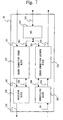
- Fig. 7 is a diagram showing the configuration of a conventional signal processor.
- a reference numeral 100 denotes a signal processor for a mobile communication system.
- the signal processor 1000 is configured with a transmitter block and a receiver block.
- the transmitter block has an error correction coder block 102 and a modulator block 104.
- the error correction coder block 102 performs error correction coding, which is the signal processing that allows correcting an error bit produced in wireless transmission, for transmission data 101 for coding as the input data.
- error correction coder block 102 outputs a coded data series 103. Error bit correction is necessary for improving line quality in wireless transmission.
- the modulator block 104 modulates the coded data series 103 as the input data so as to convert the coded data series 103 and obtain modulated transmission data 105.
- the modulator block 104 then outputs the modulated transmission data 105.
- the modulated transmission data 105 is transmitted via a wireless transmission channel. Modulation is implemented to reduce the interference effect of jamming or change of transmission channel.
- the receiver block has a demodulator block 202 and an error correction decoder block 204.
- the demodulator block 202 demodulates received modulated data 201, which is received via the wireless transmission channel, as the input data so as to convert the received modulated data 201 to obtain a demodulated data series 203.
- the demodulator block 202 then outputs the demodulated data series 203.
- Demodulation which is an inverse transform process of modulation, is a data restoration process.
- the error correction decoder block 204 performs error correction decoding for the demodulated data series 203 as the input data so as to correct an error bit produced by deterioration in line quality in wireless transmission.
- the error correction decoder block 204 then outputs decoded data 205 that is obtained through the correction.
- the error correction coder block 102, the modulator block 104, the demodulator block 202, and the error correction decoder block 204 are configured as function blocks.
- Those function blocks include devices such as DSP (Digital Signal Processor), LSI (Large Scale Integration), and FPGA (Field Programmable Gate Array). Also, those function blocks operate in various operation modes when controlled by MPU (Micro Processing Block) 302.
- wireless channel information about such as spreading code is transmitted to the modulator block 104 and the demodulator block 202 as the operation modes.
- wireless channel information about such as spreading code is transmitted to the modulator block 104 and the demodulator block 202 as the operation modes.
- the coding system if the mobile communication system is based both on convolution coding and Turbo coding, information about such as coding system and coding rate is transmitted to the error correction coder block 102 and the error correction decoder block 204 as the operation modes.
- an input/output signal line 303 is used. If the transmission is made from the MPU 302 to the error correction decoder block 204, an input/output signal line 305 is used. If an operation mode is transmitted from the MPU 302 to the modulator block 104, then the input/output signal line 303, the error correction coder block 102 and the input/output signal line 304 are used. If an operation mode is transmitted from the MPU 302 to the demodulator block 202, then the input/output signal line 305, the error correction decoder block 204, and an input/output signal line 306 are used.
- the signal processor for a mobile communication system is thus configured with the function blocks having various types of operation modes combined in a complicated manner.
- a failure occurs in such a signal processor, a necessity occurs to specify a function block as a failure factor.
- the failure is a phenomenon such as the modulated transmission data 105 or the decoded data 205 do not match with data assumed, for example.
- a human analyzer acquires debug information such as the input data and/or output data of an arbitrary function block using an externally provided debugger. This allows specifying the function blocks.
- the MPU 302 is instructed from an outside via the input/output signal line 301 connected with the MPU 302 to perform a memory read for the debug information such as the input data and/or output data of an arbitrary function block.
- the MPU 302 in response to this instruction, reads the debug information such as the input data and/or output data required from the memory provided inside or outside an arbitrary function block using the input/output signal lines 303-306 that are also used for transmitting the operation modes. Then, the MPU 302 outputs retrieved debug information using the input/output signal line 301.
- the operation mode of the signal processor changes according to the timing of CFN, which is a frame counter of 0 ⁇ 255. Then, corresponding to this change, a failure may occur.
- Another problem is, with a failure thus occurred, it is difficult, unless the debug information carries time information, to specify the timing of occurrence of the failure and the factor thereof.
- a signal processor is characterized by including:
- the dedicated output path is characterized by transmitting the debug information serially.
- the debug information is characterized by including input data to at least one of the plurality of function blocks.
- the debug information is characterized by including output data from at least one of the plurality of function blocks.
- the debug information is characterizes by being data in an arbitrary length (size).
- the signal processor is characterized by being designed for a mobile communication system, ant one of the plurality of function blocks is characterized by being an error correction coder block, which inputs transmission data for coding as input data, performs error correction coding as the signal processing, and outputs a coded data series as output data.
- the signal processor is characterized by being designed for a mobile communication system, and one of the plurality of function blocks is characterized by being a modulator block, which inputs a coded data series as input data, performs modulation as the signal processing, and outputs modulated transmission data as output data.
- the signal processor is characterized by being designed for a mobile communication system, and one of the plurality of function blocks is characterized by being a demodulator block, which inputs received modulated data as input data, performs demodulation as the signal processing, and outputs a demodulated data series as output data.
- the signal processor is characterized by being designed for a mobile communication system, and one of the plurality of function blocks is characterized by being an error correction decoder block, which inputs a decoded data series as input data, performs error bit correction as the signal processing, and outputs decoded data as output data.
- the signal processor is characterized by further including a selection multiplex output block for acquiring an instruction from an outside, selecting the debug information based on the instruction acquired, inputting the debug information selected via the dedicated output path, and outputting the debug information inputted to the outside.
- the selection multiplex output block is characterized by selecting multiple pieces of debug information based on the instruction, inputs the multiple pieces of debug information, multiplexes the multiple pieces of debug information, and outputs multiplexed debug information to the outside.
- the multiple pieces of debug information are characterized by being acquired from different function blocks.
- the selection multiplex output block is characterized by performing time multiplexing.
- the debug information is characterized by being added with time information.
- the time information is characterized by being added by a function block.
- the time information is characterized by including a plurality of frame counters of different cycles.
- the plurality of frame counters is characterized by including CFN (Connection Frame Number Counter) and BFN (Node B Frame Number Counter).
- Fig. 1 is a block diagram illustrating the configuration of a signal processor for a mobile communication system according to a first embodiment.
- Fig. 2 is a diagram showing an example of the state of output in the case where a single piece of debug information is output from an arbitrary function block.
- Fig. 3 is a diagram showing an example of the state of multiplex output in the case where multiple pieces of debug information are output from an arbitrary function block.
- Fig. 4 is a diagram showing an example of the state of output in the case where a single piece of debug information including input data and/or output data is output from an arbitrary function block, when the debug information is added with time information.
- Fig. 5 is a diagram showing an example of the state of multiplex output in the case where multiple pieces of debug information are output from one or more arbitrary function blocks, when the debug information is added with time information.
- Fig. 6 is a diagram illustrating an automation algorithm for specifying a failure factor using a debugger.
- Fig. 7 is a diagram showing the configuration of a conventional signal processor.
- Fig. 1 is a block diagram of the configuration of a signal processor for a mobile communication system according to the first embodiment.
- a reference numeral 100 denotes a signal processor for a mobile communication system.
- the signal processor 1000 is configured with a transmitter block and a receiver block.
- the transmitter block has an error correction coder block 102 and a modulator block 104.
- the error correction coder block 102 performs error correction coding, which is the signal processing that allows correcting an error bit produced in wireless transmission, for transmission data 101 for coding as the input data.
- error correction coder block 102 outputs a coded data series 103. Error bit correction is necessary for improving line quality in wireless transmission.
- the modulator block 104 modulates the coded data series 103 as the input data so as to convert the coded data series 103 and obtain modulated transmission data 105.
- the modulator block 104 then outputs the modulated transmission data 105.
- the modulated transmission data 105 is transmitted via a wireless transmission channel. Modulation is implemented to reduce the interference effect of jamming or change of transmission channel.
- the receiver block has a demodulator block 202 and an error correction decoder block 204.
- the demodulator block 202 demodulates received modulated data 201, which is received via the wireless transmission channel, as the input data so as to convert the received modulated data 201 to obtain a demodulated data series 203.
- the demodulator block 202 then outputs the demodulated data series 203.
- Demodulation which is an inverse transform process of modulation, is a data restoration process.
- the error correction decoder block 204 performs error correction decoding for the demodulated data series 203 as the input data so as to correct an error bit produced by deterioration in line quality in wireless transmission.
- the error correction decoder block 204 then outputs decoded data 205 that is obtained through the correction.
- the error correction coder block 102, the modulator block 104, the demodulator block 202, and the error correction decoder block 204 are configured as function blocks.
- Those function blocks include devices such as DSP (Digital Signal Processor), LSI (Large Scale Integration), and FPGA (Field Programmable Gate Array). Also, those function blocks operate in various operation modes when controlled by MPU (Micro Processing Block) 302.
- wireless channel information about such as spreading code is transmitted to the modulator block 104 and the demodulator block 202 as the operation modes.
- wireless channel information about such as spreading code is transmitted to the modulator block 104 and the demodulator block 202 as the operation modes.
- the coding system if the mobile communication system is based both on convolution coding and Turbo coding, information about such as coding system and coding rate is transmitted to the error correction coder block 102 and the error correction decoder block 204 as the operation modes.
- an input/output signal line 303 is used. If the transmission is made from the MPU 302 to the error correction decoder block 204, an input/output signal line 305 is used. If an operation mode is transmitted from the MPU 302 to the modulator block 104, then the input/output signal line 303, the error correction coder block 102 and the input/output signal line 304 are used. If an operation mode is transmitted from the MPU 302 to the demodulator block 202, then the input/output signal line 305, the error correction decoder block 204, and an input/output signal line 306 are used.
- the signal lines are an example of a dedicated output path, or these signal lines transmit the debug information serially.
- Signal lines 404(1) ⁇ 404(I)(where the suffix I is a positive integer 2 or more) transmit the input data and output data of the error correction coder block 102 as the debug information.
- the error correction coder block 102 as a function block has a plurality of sub-function blocks. Each signal line is connected to each sub-function block.
- Signal lines 405(1) ⁇ 405(J)(where the suffix J is a positive integer 2 or more) transmit the input data and output data of the modulator block 104 as the debug information.
- the modulator block 104 as a function block has a plurality of sub-function blocks. Each signal line is connected to each sub-function block.
- Signal lines 406(1) ⁇ 406(K)(where the suffix K is a positive integer 2 or more) transmit the input data and output data of the demodulator block 202 as the debug information.
- the demodulator block 202 as a function block has a plurality of sub-function blocks. Each signal line is connected to each sub-function block.
- Signal lines 407(1) ⁇ 407(L)(where the suffix L is a positive integer 2 or more) transmit the input data and output data of the error correction decoder block 407 as the debug information.
- the error correction decoder block 407 as a function block has a plurality of sub-function blocks. Each signal line is connected to each sub-function block.
- the signal lines 404(1) ⁇ 404(I), 405(1) ⁇ 405(J), 406(1) ⁇ 406(K), and 407(1) ⁇ 407(L) connected to the respective function blocks are connected to the selection multiplex output block 403. These signal lines can output the debug information including the input data and output data of an arbitrary function block to the selection multiplex output block 403.
- the selection multiplex output block 403 is controlled by the MPU 302 via the input/output signal line 307. Through this control, an instruction from an outside is transferred to the selection multiplex output block 403. Upon acquisition of the instruction from the outside, the selection multiplex output block 403 selects one or more items of input data and/or output data outputted by a function block arbitrarily specified as the debug information according to this instruction. The selection multiplex outputs block 403 also inputs selected debug information through the signal lines (1) ⁇ 404(I), 405(1) ⁇ 405(J), 406(1) ⁇ 406(K), and 407(1) ⁇ 407(L). Then, the selection multiplex output block 403 can output the input debug information outside the signal processor via a selection multiplex output signal line 402.
- an instruction to output the debug information including the input data and/or output data of an arbitrary function block can be given from outside the signal processor to the MPU 302 via the input/output signal line 301 connected to the MPU 3020.
- the selection multiplex output block 403 can operate according to this instruction.
- a debugger 401 for example, is externally connected to the signal processor.
- the signal lines 404(1) ⁇ 404(I), 405(1) ⁇ 405(J), 406(1) ⁇ 406, and 407(1) ⁇ 407(L) connected to the respective function blocks are provided as the dedicated output paths for outputting the debug information acquired from the respective function blocks outside the signal processor.
- the selection multiplex output block 403 including a select function and a time multiplex function is provided as an outlet for outputting the debug information outside the signal processor.
- This select function allows a fixed number of the signal lines for interfacing with the outside of the signal processor, regardless of the number of the signal lines 404(1) ⁇ 404(I), 405(1) ⁇ 405(J), 406(1) ⁇ 406(K), and 407(1) ⁇ 407(L) connected to the respective function blocks.
- this time multiplex function allows upholding the fixed number of signal lines for interfacing with the outside of the signal processor even in the case where the multiple pieces of debug information are output from one or more arbitrary function blocks.
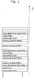
- Fig. 2 is a diagram showing an example of the state of output in the case where a single piece of debug information is output from an arbitrary function block.
- Fig. 3 is a diagram showing an example of the state of multiplex output in the case where multiple pieces of debug information are output from an arbitrary function block.
- the debug information is assumed 16 bits.
- the debug information includes a data start flag and a data length.
- the data start flag indicates a delimiter for the debug information
- the data length indicates the data length of subsequent debug information, data #1 ⁇ data #n (or data #1 ⁇ data #m).
- two pieces of debug information are time multiplexed.
- debug information a and debug information b shall be outputted alternately and serially. Those pieces of debug information may be acquired from different function blocks from each other.
- Fig. 4 is a diagram showing an example of the state of output in the case where a single piece of debug information including input data and/or output data is output from an arbitrary function block, when the debug information is added with time information. The time information is added to the debug information in the arbitrary function block.
- Fig. 5 is a diagram showing an example of the state of multiplex output in the case where multiple pieces of debug information are output from one or more arbitrary function blocks, when the debug information is added with time information. This addition is performed in the arbitrary function blocks as well.
- the debug information is assumed 16 bits.
- the debug information includes a data start flag and a data length.
- the data start flag indicates a delimiter for the debug information
- the data length indicates the data length of subsequent debug information, data #1 ⁇ data #n (or data #1 ⁇ data #m).
- Fig. 5 shows an example in which two pieces of debug information are time multiplexed. Hence debug information a and debug information b both in an arbitrary length (size) are outputted alternately and serially.
- the examples are both based on the assumption that the signal processor is designed for a mobile communication system based on the W-CDMA system prescribed by 3GPP(Third Generation Partnership Project). Based on this assumption, the debug information is added with CFN (Connection Frame Number Counter) and BFN(Node B Frame Number Counter) both as the time information.
- CFN is a frame counter of 0 ⁇ 255
- BFN is a frame counter of 0 ⁇ 4095.
- CFN is used for synchronization between UE (User Equipment) and UTRAN (UMTS Terrestrial Radio Access Network).
- UE User Equipment
- UTRAN UMTS Terrestrial Radio Access Network
- a third embodiment of the present invention will now be discussed with reference to the figures.
- a description will be given of the case where a signal processor having the functions discussed in the first or second embodiment is combined with the debugger 401 of Fig. 1. Combining with the debugger 401 has the effect that a failure factor can be automatically specified.
- the debugger of Fig. 1 has the function of instructing the MPU 302 to output the debug information to an arbitrary function block via the input/output signal line 301.
- the MPU 302 based on this instruction, controls the selection multiplex output block 403 via the input/output signal line 307.
- the debugger has the function of retrieving debug information that is outputted as a result of the control via the selection multiplex output signal line 402.
- Fig. 6 is a diagram illustrating an automation algorithm using a debugger for specifying a failure factor. More particularly, this algorithm is used to specify a function block having a failure factor and to specify the timing thereof.
- the debugger (401) outputs an instruction to the MPU (302) to start outputting debug information to an arbitrary function block via the input/output signal line 301, and then a memory write is performed of the instruction. Note, however, if the current process is processed for a second time or more, then the instruction to start outputting the debug information is sent to a function block that has not been subjected to 605 judgement.
- the MPU (302) transmits to the selection multiplex output block (403) via the input/output signal line 307 a control order indicating which of the signal lines 404(1) ⁇ 404(I), 405(1) ⁇ 405(J), 406(1) ⁇ 406(K), and 407(1) ⁇ 407(L) connected to the respective function blocks, is selected, and indicating whether or not data output is with time multiplex.
- the debugger (401) receives debug information outputted from the signal processor (100) via the selection multiplex output signal line 402, and writes it in an internal memory of the debugger (401).
- the debugger (401) outputs an instruction to the MPU (302) to stop outputting the debug information to the arbitrary function block via the input/output signal line 301, and a memory write is performed of the instruction.
- the dedicated output paths are thus provided for transmitting the debug information acquired from the function blocks serially.
- the debug information required may be obtained independent of the memory capacity.
- the debug information is thus multiplexed.
- the configuration of the interface with the outside may be simplified.
- the time information is thus added to the debug information. Hence, the specification of the timing of a failure occurrence may be facilitated.
- the frame counters of a different cycle are added as the time information. Hence, the timing may be specified for a long range.
Landscapes
- Engineering & Computer Science (AREA)
- Theoretical Computer Science (AREA)
- Computer Hardware Design (AREA)
- Quality & Reliability (AREA)
- Physics & Mathematics (AREA)
- General Engineering & Computer Science (AREA)
- General Physics & Mathematics (AREA)
- Debugging And Monitoring (AREA)
- Mobile Radio Communication Systems (AREA)
- Detection And Prevention Of Errors In Transmission (AREA)
Abstract
Description
Claims (17)
- A signal processor comprising:(1) a plurality of function blocks for signal processing; and(2) a dedicated output path for transmitting debug information for debugging for the signal processor obtained from each of the plurality of function blocks.
- The signal processor according to claim 1, wherein the dedicated output path transmits the debug information serially.
- The signal processor according to claim 1, wherein the debug information includes input data to at least one of the plurality of function blocks.
- The signal processor according to claim 1, wherein the debug information includes output data from at least one of the plurality of function blocks.
- The signal processor according to claim 1, wherein the debug information is data in an arbitrary length (size).
- The signal processor according to claim 1, wherein the signal processor is designed for a mobile communication system, and
wherein one of the plurality of function blocks is an error correction coder block, which inputs transmission data for coding as input data, performs error correction coding as the signal processing, and outputs a coded data series as output data. - The signal processor according to claim 1, wherein the signal processor is designed for a mobile communication system, and
wherein one of the plurality of function blocks is a modulator block, which inputs a coded data series as input data, performs modulation as the signal processing, and outputs modulated transmission data as output data. - The signal processor according to claim 1, wherein the signal processor is designed for a mobile communication system, and
wherein one of the plurality of function blocks is a demodulator block, which inputs received modulated data as input data, performs demodulation as the signal processing, and outputs a demodulated data series as output data. - The signal processor according to claim 1, wherein the signal processor is designed for a mobile communication system, and
wherein one of the plurality of function blocks is an error correction decoder block, which inputs a decoded data series as input data, performs error bit correction as the signal processing, and outputs decoded data as output data. - The signal processor according to claim 1, further comprising:a selection multiplex output block for acquiring an instruction from an outside, selecting the debug information based on the instruction acquired, inputting the debug information selected via the dedicated output path, and outputting the debug information inputted to the outside.
- The signal processor according to claim 10, wherein the selection multiplex output block selects multiple pieces of debug information based on the instruction, inputs the multiple pieces of debug information, multiplexes the multiple pieces of debug information, and outputs multiplexed debug information to the outside.
- The signal processor according to claim 11, wherein the multiple pieces of debug information are acquired from different function blocks.
- The signal processor according to claim 10, wherein the selection multiplex output block performs time multiplexing.
- The signal processor according to claim 1, wherein the debug information is added with time information.
- The signal processor according to claim 14, wherein the time information is added by a function block.
- The signal processor according to claim 15, wherein the time information includes a plurality of frame counters of different cycles.
- The signal processor according to claim 16, wherein the plurality of frame counters includes CFN (Connection Frame Number Counter) and BFN (Node B Frame Number Counter).
Applications Claiming Priority (1)
| Application Number | Priority Date | Filing Date | Title |
|---|---|---|---|
| PCT/JP2002/005186 WO2003100615A1 (en) | 2002-05-29 | 2002-05-29 | Signal processor |
Publications (2)
| Publication Number | Publication Date |
|---|---|
| EP1508857A1 true EP1508857A1 (en) | 2005-02-23 |
| EP1508857A4 EP1508857A4 (en) | 2008-11-05 |
Family
ID=29561089
Family Applications (1)
| Application Number | Title | Priority Date | Filing Date |
|---|---|---|---|
| EP02733237A Withdrawn EP1508857A4 (en) | 2002-05-29 | 2002-05-29 | SIGNAL PROCESSOR |
Country Status (5)
| Country | Link |
|---|---|
| US (1) | US20050195890A1 (en) |
| EP (1) | EP1508857A4 (en) |
| JP (1) | JPWO2003100615A1 (en) |
| CN (1) | CN1628288A (en) |
| WO (1) | WO2003100615A1 (en) |
Families Citing this family (2)
| Publication number | Priority date | Publication date | Assignee | Title |
|---|---|---|---|---|
| US10075266B2 (en) * | 2013-10-09 | 2018-09-11 | Qualcomm Incorporated | Data transmission scheme with unequal code block sizes |
| CN112104382A (en) * | 2020-09-10 | 2020-12-18 | 中国电子科技集团公司第五十八研究所 | Parallel digital down-conversion processing system based on digital signals |
Family Cites Families (12)
| Publication number | Priority date | Publication date | Assignee | Title |
|---|---|---|---|---|
| JPH06214819A (en) * | 1993-01-19 | 1994-08-05 | Toshiba Corp | Information processor and system and method for evaluating the same |
| JPH06284464A (en) * | 1993-03-25 | 1994-10-07 | Toshiba Corp | Dual mode radio communication device |
| JPH07260885A (en) * | 1994-03-18 | 1995-10-13 | Fujitsu Ltd | Electronics |
| JPH09504673A (en) * | 1994-06-06 | 1997-05-06 | エリクソン インコーポレイテッド | Self-regulating modulator |
| JPH0964811A (en) * | 1995-08-28 | 1997-03-07 | Sony Corp | Transmit / receive signal monitoring method |
| US5717695A (en) * | 1995-12-04 | 1998-02-10 | Silicon Graphics, Inc. | Output pin for selectively outputting one of a plurality of signals internal to a semiconductor chip according to a programmable register for diagnostics |
| US5911082A (en) * | 1997-02-25 | 1999-06-08 | Audio Digitalimaging Inc. | Parallel processing building block chip |
| IL128933A0 (en) * | 1999-03-11 | 2000-02-17 | Mango Computers Ltd | A system for convertinog high-level computer languages into specific low-level languages of digital signal processors |
| JP2000349654A (en) * | 1999-03-31 | 2000-12-15 | Matsushita Electric Ind Co Ltd | Transmission device, reception device, and transmission / reception method |
| US6684348B1 (en) * | 1999-10-01 | 2004-01-27 | Hitachi, Ltd. | Circuit for processing trace information |
| JP4212224B2 (en) * | 2000-07-10 | 2009-01-21 | 株式会社東芝 | Semiconductor integrated circuit |
| US20020133794A1 (en) * | 2001-02-24 | 2002-09-19 | Ruban Kanapathippillai | Method and apparatus for integrated circuit debugging |
-
2002
- 2002-05-29 EP EP02733237A patent/EP1508857A4/en not_active Withdrawn
- 2002-05-29 US US10/508,846 patent/US20050195890A1/en not_active Abandoned
- 2002-05-29 CN CNA028290348A patent/CN1628288A/en active Pending
- 2002-05-29 JP JP2004508000A patent/JPWO2003100615A1/en active Pending
- 2002-05-29 WO PCT/JP2002/005186 patent/WO2003100615A1/en not_active Ceased
Also Published As
| Publication number | Publication date |
|---|---|
| JPWO2003100615A1 (en) | 2005-09-29 |
| EP1508857A4 (en) | 2008-11-05 |
| CN1628288A (en) | 2005-06-15 |
| WO2003100615A1 (en) | 2003-12-04 |
| US20050195890A1 (en) | 2005-09-08 |
Similar Documents
| Publication | Publication Date | Title |
|---|---|---|
| US10362220B2 (en) | Conversation of pixel data into compression format of pixels | |
| RU2371883C2 (en) | System and method for multiplexing of control data at physical data link | |
| EP2317677B1 (en) | Radio transmission method and radio transmission device | |
| AU733218B2 (en) | Method for decreasing the frame error rate in data transmission in the form of data frames | |
| TW201419784A (en) | Fixed HS-DSCH or E-DCH configuration for VOIP (1) | |
| NO317235B1 (en) | Method and apparatus for voice transmission in a mobile communication system | |
| JP4015465B2 (en) | Method for transmitting signaling information over a control channel of a communication system | |
| US20230085423A1 (en) | Packet communication system, and its transmitting apparatus, receiving apparatus, and program | |
| US7653844B2 (en) | Communication apparatus and communication system | |
| EP1300976B1 (en) | Method of blind transport format detection | |
| EP1508857A1 (en) | Signal processor | |
| JP2020519204A (en) | Communication method and communication device | |
| US5333197A (en) | System to prevent a scrambler from generating undesired symbols | |
| JP4258272B2 (en) | CDMA receiver and its TFCI candidate determination method | |
| JP2004349763A (en) | Code division multiple access receiving apparatus | |
| US6198499B1 (en) | Radio-communication video terminal device | |
| JP2022019960A (en) | Receiver, transmitter, receiving method and transmitting method | |
| JP4905720B2 (en) | TFCI decoding apparatus and method | |
| KR20040059165A (en) | Emulator in communication system | |
| JP3267581B2 (en) | Frame synchronization method and apparatus | |
| JP2006318451A (en) | Method and system for screen frame transmission from one terminal to multiple terminals, and receiving device thereof | |
| EP1047221A2 (en) | PN code generator, communication unit using the PN code generator, communication system, and PN code generation method | |
| JP3135546B2 (en) | Error correction circuit | |
| JP3587372B2 (en) | Serial communication method and device | |
| KR20010068526A (en) | Method and apparatus for time based data coding for communication systems |
Legal Events
| Date | Code | Title | Description |
|---|---|---|---|
| PUAI | Public reference made under article 153(3) epc to a published international application that has entered the european phase |
Free format text: ORIGINAL CODE: 0009012 |
|
| 17P | Request for examination filed |
Effective date: 20041126 |
|
| AK | Designated contracting states |
Kind code of ref document: A1 Designated state(s): AT BE CH CY DE DK ES FI FR GB GR IE IT LI LU MC NL PT SE TR |
|
| AX | Request for extension of the european patent |
Extension state: AL LT LV MK RO SI |
|
| DAX | Request for extension of the european patent (deleted) | ||
| RBV | Designated contracting states (corrected) |
Designated state(s): DE FR GB |
|
| RAP1 | Party data changed (applicant data changed or rights of an application transferred) |
Owner name: MITSUBISHI DENKI KABUSHIKI KAISHA |
|
| A4 | Supplementary search report drawn up and despatched |
Effective date: 20081006 |
|
| 17Q | First examination report despatched |
Effective date: 20090318 |
|
| STAA | Information on the status of an ep patent application or granted ep patent |
Free format text: STATUS: THE APPLICATION HAS BEEN WITHDRAWN |
|
| 18W | Application withdrawn |
Effective date: 20090907 |