EP1507406B1 - Image sensor with active reset and randomly addressable pixels - Google Patents
Image sensor with active reset and randomly addressable pixels Download PDFInfo
- Publication number
- EP1507406B1 EP1507406B1 EP04005865A EP04005865A EP1507406B1 EP 1507406 B1 EP1507406 B1 EP 1507406B1 EP 04005865 A EP04005865 A EP 04005865A EP 04005865 A EP04005865 A EP 04005865A EP 1507406 B1 EP1507406 B1 EP 1507406B1
- Authority
- EP
- European Patent Office
- Prior art keywords
- reset
- column
- operational amplifier
- imaging array
- line
- Prior art date
- Legal status (The legal status is an assumption and is not a legal conclusion. Google has not performed a legal analysis and makes no representation as to the accuracy of the status listed.)
- Expired - Fee Related
Links
Images

Classifications
-
- H—ELECTRICITY
- H04—ELECTRIC COMMUNICATION TECHNIQUE
- H04N—PICTORIAL COMMUNICATION, e.g. TELEVISION
- H04N25/00—Circuitry of solid-state image sensors [SSIS]; Control thereof
- H04N25/60—Noise processing, e.g. detecting, correcting, reducing or removing noise
- H04N25/65—Noise processing, e.g. detecting, correcting, reducing or removing noise applied to reset noise, e.g. KTC noise related to CMOS structures by techniques other than CDS
-
- H—ELECTRICITY
- H04—ELECTRIC COMMUNICATION TECHNIQUE
- H04N—PICTORIAL COMMUNICATION, e.g. TELEVISION
- H04N25/00—Circuitry of solid-state image sensors [SSIS]; Control thereof
- H04N25/70—SSIS architectures; Circuits associated therewith
-
- H—ELECTRICITY
- H04—ELECTRIC COMMUNICATION TECHNIQUE
- H04N—PICTORIAL COMMUNICATION, e.g. TELEVISION
- H04N25/00—Circuitry of solid-state image sensors [SSIS]; Control thereof
- H04N25/70—SSIS architectures; Circuits associated therewith
- H04N25/76—Addressed sensors, e.g. MOS or CMOS sensors
- H04N25/77—Pixel circuitry, e.g. memories, A/D converters, pixel amplifiers, shared circuits or shared components
Definitions
- the present invention relates to CMOS image sensors.
- CMOS image sensors provide a number of advantages over CCD image sensors.
- the CMOS yields are significantly better than those of the CCD fabrication process.
- the minimum noise levels achievable with CMOS-based sensors are substantially lower than those that can be obtained with CCDs.
- the image stored in a.CMOS-based image sensor can be readout without destroying the image.
- CMOS sensors suffer from temporal noise.
- Schemes for reducing temporal noise are known to the art.
- U.S. Patent 6,424,375 which is hereby incorporated by reference, describes an active pixel reset system that reduces the effects of temporal noise.
- the pixel design discussed in this patent requires a CMOS pixel having a number of additional components that are used to reset the voltage on a photodiode prior to accumulating an image. This additional circuitry increases the size of the pixel, and hence, increases the cost of an imaging array utilizing this design.
- CMOS image sensor comprising a photodiode for carrying out a photoelectric conversion of incident light, a reset transistor for resetting the voltage at a cathode of the photodiode and a voltage control circuit for controlling the potential of a gate of the reset transistor during a reset cycle to thereby vary the on-state resistance of the reset transistor in order to reduce the kTC noise whilst achieving a high bandwidth.
- the present invention is based on the object of providing an imaging array having a reduced noise and a further increased bandwidth.
- the present invention includes an imaging array having one or more columns of pixels.
- Each pixel includes a photodiode including first and second terminals, a local reset circuit for connecting the first terminal to a column reset line; and a buffer circuit for selectively connecting the first terminal to a column bit line in response to a word select signal.
- Each column also includes a column reset circuit having an operational amplifier and a low-pass filter.
- the operational amplifier has a first input connected to the column bit line for that column and a second input connected to a reset signal generator that generates a reset signal during a reset cycle.
- the output of the operational amplifier is connected to the column reset line during the reset cycle.
- the operational amplifier has a gain that is determined by a gain control signal.
- the gain of the operational amplifier is varied during the reset cycle in this embodiment.
- the passband of the low-pass filter is also varied over the reset cycle.
- the preferred low-pass filter includes one or more capacitors that are connected to the column reset line during the reset cycle.
- Figure 1 is a schematic drawing of one column 100 of pixels in a two-dimensional imaging array.
- an imaging array is constructed from a plurality of pixels that are organized into a rectangular array having M columns and N rows.
- Figure 1 shows one column of pixels. Exemplary pixels are shown at 131 and 134.
- Each pixel has three components, a photodiode 112, a local reset circuit 101, and an output amplifier.
- the output amplifier consists of transistors 114 and 116.
- Transistor 116 is used to selectively couple the output from transistor 114 to a column output line 118 that is used to couple a signal representing the potential on photodiode 112 to a column output amplifier 61.
- the selected pixel is connected to output line 118 by a signal on the corresponding word line 121.
- the local reset circuit 101 consists of transistors 122 and 108 and capacitor 111. While capacitor 111 is shown as a separate circuit component, it should be noted that capacitor 111 can be replaced by the parasitic capacitance of transistor 122 in some embodiments.
- Transistor 122 couples the gate of transistor 108 to a column reset line 158 in response to a signal on the corresponding reset line. Exemplary word reset lines are shown at 141 and 151. At any given time, only one pixel in each column is coupled to column reset line 158.
- Each column of pixels also includes a column reset circuit 60 that includes an amplifier 40 and a capacitor 30.
- amplifier 40 includes a plurality of operational amplifiers connected in parallel. Exemplary amplifiers are shown at 41 and 42. Each amplifier includes a gating circuit that determines if the amplifier is ON or OFF. The gating circuits for amplifiers 41 and 42 are controlled by suitable signals on control lines 44 and 45, respectively.
- capacitor 30 is constructed from a plurality of capacitors connected in parallel. Exemplary capacitors are shown at 31 and 32. Each capacitor has a corresponding switch that determines whether or not the capacitor is connected to column reset line 158. The switches corresponding to capacitors 31 and 32 are shown at 33 and 34, respectively.
- column reset line 158 e.g., amplifier 41 and capacitor 31.
- pixel 134 is to be reset.
- the reset cycle can be broken into two time periods.
- column reset line 158 is connected to the reset amplifier by closing switch 50.
- reset line 151 is raised to connect the gate of transistor 108 to reset line 158, and transistor 108 is connected to Vdd via reset line 152.
- the output of amplifier 41 is then briefly grounded.
- Amplifier 41 is then connected to a reset signal generator via lead 43.
- Vr the negative input of the operational amplifier
- Vr exceeds the potential on photodiode 112 plus the threshold voltages of transistors 108 and 114, the potential on the photodiode likewise increases to some maximum value.
- Vr is held constant at its maximum value.
- the potential on photodiode 112 increases during this period of time due to transistor 108.
- the drop in potential on reset line 158 turns off transistor 108 and the potential on photodiode 112 is then allowed to settle during the second period of time.
- the photodiode is capacitive coupled to reset line 158 via the gate to source capacitance of transistor 108.
- the capacitive coupling to photodiode 112 forms a feedback loop around amplifier 41.
- This feedback loop is used to reduce the reset noise on the photodiode 112.
- the settling of the feedback loop follows a typical RC time curve, hence, the larger the capacitance, the longer the settling time.
- this problem is overcome by using an amplifier having an amplification factor that varies in time over the reset cycle.
- the bandwidth limiting capacitance is also varied over time.
- a small amplification factor and large bandwidth are utilized to move the potential on photodiode 112 to a value close to the desired reset potential.
- a larger amplification factor and a smaller bandwidth are utilized to reduce the noise level. Since the reset potential is near its final value when the switch occurs, the settling time is not increased significantly, since the voltage change that must be accommodated at the reduced bandwidth is relatively small.
- the change in amplification and bandwidth limiting capacitance is implemented by switching the selected amplifier and capacitor.
- amplifier 40 includes a plurality of operational amplifiers. Each operational amplifier has a different gain in this embodiment of the present invention. Hence, by switching the selected amplifier during the reset cycle, the amplification factor can be effectively varied.
- capacitor 30 is implemented as a plurality of capacitors that can be switched into, or out of, the reset loop at predetermined points in the reset cycle.
- Imaging array 300 is constructed from a plurality of columns of pixels constructed as discussed above with reference to Figure 1.
- the pixels are organized into a rectangular array 301 having N columns and M rows. All of the pixels on a given row are connected to the same word line and word reset line.
- Each column of pixels has one reset circuit such as that discussed with reference to Figure 1.
- the N column reset circuits are shown at 302.
- An exemplary column of pixels is shown at 310, and the corresponding column reset circuit is shown at 311.
- An exemplary row is shown at 312.
- a single reset signal generator 303 provides the reset signal for all of the columns.
- the readout circuitry includes an analog-to-digital converter (ADC) that converts the analog value to a digital value that is output from the imaging array.
- ADC analog-to-digital converter
- the readout circuit can include one ADC per column.
- the ADC latches preferably store the converted results. The results can then be readout in an order specified by column select circuit 304.
- the present invention is well suited for applications in which only a subset of all of the pixels in the array are utilized.
- the camera sets the focus and exposure by examining a subset of the pixels in an image.
- the focus is typically set with reference to one of a predetermined plurality of subfields in the field of view.
- the exposure is typically set by measuring the light intensity of a predetermined plurality of pixels that are more or less randomly placed in the field of view.
- the present invention allows all or a subset of the pixels in each row to be readout. Similarly, any subset of the pixels in any given row can be reset. Hence, when a sequence of measurement that involves only a subset of the total pixels is needed, only those pixels need to be read and reset. Since reading and resetting the entire image can require a significant amount of time, this random access feature can significantly shorten the time needed to compute the correct exposure and focus.
- the power consumed in such partial readout and reset operations is substantially less than that utilized in systems in which all of the image must be read and reset.
- Digital cameras are generally powered by batteries.
- the present invention provides a means for increasing the number of images that can be taken before the battery needs to be replaced.
Description
- The present invention relates to CMOS image sensors.
- In principle, CMOS image sensors provide a number of advantages over CCD image sensors. The CMOS yields are significantly better than those of the CCD fabrication process. In addition, the minimum noise levels achievable with CMOS-based sensors are substantially lower than those that can be obtained with CCDs. Finally, the image stored in a.CMOS-based image sensor can be readout without destroying the image.
- CMOS sensors suffer from temporal noise. Schemes for reducing temporal noise are known to the art. For example, U.S. Patent 6,424,375, which is hereby incorporated by reference, describes an active pixel reset system that reduces the effects of temporal noise. However, the pixel design discussed in this patent requires a CMOS pixel having a number of additional components that are used to reset the voltage on a photodiode prior to accumulating an image. This additional circuitry increases the size of the pixel, and hence, increases the cost of an imaging array utilizing this design.
- In addition, there is a tradeoff between the degree of noise reduction and the time needed to reset the pixel. To provide high noise reduction, the bandwidth of the reset circuit must be limited. This increases the time needed for the photodiode to stabilize at the reset potential. If the bandwidth is increased to provide a shorter reset time, the noise level increases. Hence, this design cannot provide both short reset times and high noise reduction.
- US 2003/146993 discloses a CMOS image sensor comprising a photodiode for carrying out a photoelectric conversion of incident light, a reset transistor for resetting the voltage at a cathode of the photodiode and a voltage control circuit for controlling the potential of a gate of the reset transistor during a reset cycle to thereby vary the on-state resistance of the reset transistor in order to reduce the kTC noise whilst achieving a high bandwidth.
- The present invention is based on the object of providing an imaging array having a reduced noise and a further increased bandwidth.
- This object is achieved by an imaging array in accordance with
claim 1. - The present invention includes an imaging array having one or more columns of pixels. Each pixel includes a photodiode including first and second terminals, a local reset circuit for connecting the first terminal to a column reset line; and a buffer circuit for selectively connecting the first terminal to a column bit line in response to a word select signal. Each column also includes a column reset circuit having an operational amplifier and a low-pass filter. The operational amplifier has a first input connected to the column bit line for that column and a second input connected to a reset signal generator that generates a reset signal during a reset cycle. The output of the operational amplifier is connected to the column reset line during the reset cycle. In one embodiment, the operational amplifier has a gain that is determined by a gain control signal. The gain of the operational amplifier is varied during the reset cycle in this embodiment. In this embodiment, the passband of the low-pass filter is also varied over the reset cycle. The preferred low-pass filter includes one or more capacitors that are connected to the column reset line during the reset cycle.
-
- Figure 1 is a schematic drawing of one
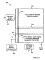
column 100 of pixels in a two-dimensional imaging array. - Figure 2 is a block diagram of a two-
dimensional imaging array 300 together with the reset and decode circuitry used to run the pixels of the imaging array. - The manner in which the present invention provides its advantages can be more easily understood with reference to Figure 1. Figure 1 is a schematic drawing of one
column 100 of pixels in a two-dimensional imaging array. - Referring to Figure 1, an imaging array according to one embodiment of the present invention is constructed from a plurality of pixels that are organized into a rectangular array having M columns and N rows. Figure 1 shows one column of pixels. Exemplary pixels are shown at 131 and 134. Each pixel has three components, a
photodiode 112, alocal reset circuit 101, and an output amplifier. The output amplifier consists oftransistors Transistor 116 is used to selectively couple the output fromtransistor 114 to acolumn output line 118 that is used to couple a signal representing the potential onphotodiode 112 to acolumn output amplifier 61. The selected pixel is connected tooutput line 118 by a signal on thecorresponding word line 121. - The
local reset circuit 101 consists oftransistors capacitor 111. Whilecapacitor 111 is shown as a separate circuit component, it should be noted thatcapacitor 111 can be replaced by the parasitic capacitance oftransistor 122 in some embodiments.Transistor 122 couples the gate oftransistor 108 to a column reset line 158 in response to a signal on the corresponding reset line. Exemplary word reset lines are shown at 141 and 151. At any given time, only one pixel in each column is coupled to column reset line 158. - Each column of pixels also includes a
column reset circuit 60 that includes anamplifier 40 and acapacitor 30. In the embodiment of the present invention shown in Figure 1,amplifier 40 includes a plurality of operational amplifiers connected in parallel. Exemplary amplifiers are shown at 41 and 42. Each amplifier includes a gating circuit that determines if the amplifier is ON or OFF. The gating circuits foramplifiers control lines capacitor 30 is constructed from a plurality of capacitors connected in parallel. Exemplary capacitors are shown at 31 and 32. Each capacitor has a corresponding switch that determines whether or not the capacitor is connected to column reset line 158. The switches corresponding tocapacitors - To better understand the basic reset cycle, assume that only one of the component amplifiers and capacitors is connected to column reset line 158, e.g.,
amplifier 41 andcapacitor 31. Assume thatpixel 134 is to be reset. The reset cycle can be broken into two time periods. At the start of the reset cycle, column reset line 158 is connected to the reset amplifier byclosing switch 50. In addition,reset line 151 is raised to connect the gate oftransistor 108 to reset line 158, andtransistor 108 is connected to Vdd viareset line 152. The output ofamplifier 41 is then briefly grounded.Amplifier 41 is then connected to a reset signal generator vialead 43. During the first time period the negative input of the operational amplifier, Vr, is increased linearly to a maximum potential. When Vr exceeds the potential onphotodiode 112 plus the threshold voltages oftransistors photodiode 112 increases during this period of time due totransistor 108. This causes the output ofamplifier 41, which is connected to the reset line 158, to fall until its differential inputs are at approximately the same potential. The drop in potential on reset line 158 turns offtransistor 108 and the potential onphotodiode 112 is then allowed to settle during the second period of time.
During this second time period, the photodiode is capacitive coupled to reset line 158 via the gate to source capacitance oftransistor 108. The capacitive coupling to photodiode 112 forms a feedback loop aroundamplifier 41. This feedback loop is used to reduce the reset noise on thephotodiode 112. The settling of the feedback loop follows a typical RC time curve, hence, the larger the capacitance, the longer the settling time. - The noise level, i.e., the variations in the reset potential on the photodiode, also depends on the value of
capacitor 31. It can be shown that the noise in the reset value is approximately given by:
where kT is Boltzmann's constant times absolute temperature, C is the capacitance of thephotodiode 112, A is the amplification factor ofamplifier 41, β is the feedback loop gain, and f is a function of the bandwidth of the reset loop that increases with increasing bandwidth. Hence, to provide the lowest noise, one wishes to maximize the amplification factor while minimizing the bandwidth of the reset loop. The bandwidth of the reset loop is controlled by the capacitance ofcapacitor 31 in this example. The larger the output capacitance ofamplifier 40, the smaller the amplifier bandwidth. In addition, a small bandwidth must be used if a large amplification factor is utilized to minimize the noise arising from the first term in the above equation. Unfortunately, as noted above, the time needed for the photodiode to settle to the reset potential is also determined by the bandwidth of the reset loop, smaller bandwidths lead to increased settling times. Hence, a single amplifier and capacitance value cannot provide both low noise and fast reset times. - In one preferred embodiment of the invention, this problem is overcome by using an amplifier having an amplification factor that varies in time over the reset cycle. Similarly, the bandwidth limiting capacitance is also varied over time. In the beginning of the reset cycle, a small amplification factor and large bandwidth are utilized to move the potential on
photodiode 112 to a value close to the desired reset potential. Once the reset potential is close to its final value, a larger amplification factor and a smaller bandwidth are utilized to reduce the noise level. Since the reset potential is near its final value when the switch occurs, the settling time is not increased significantly, since the voltage change that must be accommodated at the reduced bandwidth is relatively small. - In this embodiment, the change in amplification and bandwidth limiting capacitance is implemented by switching the selected amplifier and capacitor. As noted above,
amplifier 40 includes a plurality of operational amplifiers. Each operational amplifier has a different gain in this embodiment of the present invention. Hence, by switching the selected amplifier during the reset cycle, the amplification factor can be effectively varied. Similarly,capacitor 30 is implemented as a plurality of capacitors that can be switched into, or out of, the reset loop at predetermined points in the reset cycle. - Refer now to Figure 2, which is a block diagram of a two-
dimensional imaging array 300 together with the reset and decode circuitry used to run the pixels of the imaging array.Imaging array 300 is constructed from a plurality of columns of pixels constructed as discussed above with reference to Figure 1. The pixels are organized into arectangular array 301 having N columns and M rows. All of the pixels on a given row are connected to the same word line and word reset line. Each column of pixels has one reset circuit such as that discussed with reference to Figure 1. The N column reset circuits are shown at 302. An exemplary column of pixels is shown at 310, and the corresponding column reset circuit is shown at 311. An exemplary row is shown at 312. A singlereset signal generator 303 provides the reset signal for all of the columns. - All of the pixels in a row can be read and reset in parallel. The row in question is determined by an address that is input to word decode
circuit 305. When a row is selected for reading, N analog signals are available for reading, one from each column. If a single pixel value is to be output, acolumn decode circuit 304 can be utilized to select the desired column. In one preferred embodiment of the invention, the readout circuitry includes an analog-to-digital converter (ADC) that converts the analog value to a digital value that is output from the imaging array. However, embodiments that output the analog voltage that is converted off of the imaging array can also be practiced. - Alternatively, the readout circuit can include one ADC per column. In this case, the ADC latches preferably store the converted results. The results can then be readout in an order specified by column
select circuit 304. - It should be noted that the present invention is well suited for applications in which only a subset of all of the pixels in the array are utilized. For example, in automated digital cameras, the camera sets the focus and exposure by examining a subset of the pixels in an image. The focus is typically set with reference to one of a predetermined plurality of subfields in the field of view. The exposure is typically set by measuring the light intensity of a predetermined plurality of pixels that are more or less randomly placed in the field of view.
- The present invention allows all or a subset of the pixels in each row to be readout. Similarly, any subset of the pixels in any given row can be reset. Hence, when a sequence of measurement that involves only a subset of the total pixels is needed, only those pixels need to be read and reset. Since reading and resetting the entire image can require a significant amount of time, this random access feature can significantly shorten the time needed to compute the correct exposure and focus.
- In addition, the power consumed in such partial readout and reset operations is substantially less than that utilized in systems in which all of the image must be read and reset. Digital cameras are generally powered by batteries. Hence, the present invention provides a means for increasing the number of images that can be taken before the battery needs to be replaced.
- Various modifications to the present invention will become apparent to those skilled in the art from the foregoing description and accompanying drawings. Accordingly, the present invention is to be limited solely by the scope of the following claims.
Claims (7)
- An imaging array comprising:a first plurality of pixels (131, 134), each pixel comprising:a photodiode (112) including first and second terminals;a local reset circuit (101) for connecting said first terminal to a first column reset line (158); anda buffer circuit (114, 116) for selectively connecting said first terminal to a first column bit line (118) in response to a word select signal; anda first column reset circuit (60) comprising an operational amplifier (40) having an amplification factor and a low-pass filter (30) having a passband, said operational amplifier (40) having a first input connected to said first column bit line (118), a second input connected to a reset signal generator that generates a reset signal during a reset cycle, and an output selectively connected to said first column reset line (158);wherein said reset signal generator is adapted for controlling said amplification factor and/or said passband during said reset cycle.
- The imaging array of Claim 1 wherein said operational amplifier (40) has a gain that is determined by a gain control signal.
- The imaging array of Claim 2 wherein said operational amplifier (40) comprises a plurality of component operational amplifiers (41, 42) connected in parallel, each component operational amplifier (41, 42) having a different gain, each component operational amplifier being selectable by said gain control signal.
- The imaging array of Claim 2 wherein said gain of said operational amplifier (40) is varied during said reset cycle.
- The imaging array of Claim 1 wherein said low-pass filter passband of said low-pass filter (30) is determined by low-pass filter control signal.
- The imaging array of Claim 1 wherein said low-pass filter comprises a capacitor (31, 32) that is connected to said first column reset line (158) during said reset cycle.
- The imaging array of Claim 1 further comprising:a second plurality of pixels (131, 134), each pixel comprising:a photodiode (112) including first and second terminals;a local reset circuit (101) for connecting said first terminal to a second column reset line (158); anda buffer circuit (114, 116) for selectively connecting said second terminal to a second column bit line (118) in response to a word select signal; anda second column reset circuit (60) comprising an operational amplifier (40) and a low-pass filter (30), said operational amplifier (40) having a first input connected to said second column bit line, a second input connected to said reset signal, and an output selectively connected to said second column reset line (158).
Applications Claiming Priority (2)
| Application Number | Priority Date | Filing Date | Title |
|---|---|---|---|
| US10/639,227 US7274397B2 (en) | 2003-08-11 | 2003-08-11 | Image sensor with active reset and randomly addressable pixels |
| US639227 | 2003-08-11 |
Publications (2)
| Publication Number | Publication Date |
|---|---|
| EP1507406A1 EP1507406A1 (en) | 2005-02-16 |
| EP1507406B1 true EP1507406B1 (en) | 2006-02-08 |
Family
ID=33565227
Family Applications (1)
| Application Number | Title | Priority Date | Filing Date |
|---|---|---|---|
| EP04005865A Expired - Fee Related EP1507406B1 (en) | 2003-08-11 | 2004-03-11 | Image sensor with active reset and randomly addressable pixels |
Country Status (6)
| Country | Link |
|---|---|
| US (1) | US7274397B2 (en) |
| EP (1) | EP1507406B1 (en) |
| JP (1) | JP4487248B2 (en) |
| CN (1) | CN100546337C (en) |
| DE (1) | DE602004000375T2 (en) |
| TW (1) | TWI341122B (en) |
Families Citing this family (14)
| Publication number | Priority date | Publication date | Assignee | Title |
|---|---|---|---|---|
| US20060102827A1 (en) * | 2004-11-17 | 2006-05-18 | Matsushita Electric Industrial Co., Ltd. | Solid-state imaging device |
| US7728896B2 (en) * | 2005-07-12 | 2010-06-01 | Micron Technology, Inc. | Dual conversion gain gate and capacitor and HDR combination |
| US20070024713A1 (en) * | 2005-07-28 | 2007-02-01 | Baer Richard L | Imaging parallel interface RAM |
| US7750960B2 (en) * | 2006-03-15 | 2010-07-06 | Honeywell International Inc. | System and apparatus for high dynamic range sensor |
| US20090040351A1 (en) * | 2007-08-09 | 2009-02-12 | Micron Technology, Inc. | Method and apparatus for reducing noise in a pixel array |
| CN101877758B (en) * | 2009-04-28 | 2013-04-03 | 英属开曼群岛商恒景科技股份有限公司 | Read-out system and method of image sensor |
| JP5530277B2 (en) | 2010-07-09 | 2014-06-25 | パナソニック株式会社 | Solid-state imaging device and driving method thereof |
| JP5470181B2 (en) | 2010-07-09 | 2014-04-16 | パナソニック株式会社 | Solid-state imaging device |
| US8390712B2 (en) | 2010-12-08 | 2013-03-05 | Aptina Imaging Corporation | Image sensing pixels with feedback loops for imaging systems |
| US20120242621A1 (en) * | 2011-03-24 | 2012-09-27 | Christopher James Brown | Image sensor and display device incorporating the same |
| US8952729B2 (en) | 2013-04-03 | 2015-02-10 | BAE Systems Imaging Solutions Inc. | Sample and hold circuit with reduced noise |
| CN106341627B (en) * | 2015-07-07 | 2020-08-11 | 松下知识产权经营株式会社 | Image pickup apparatus |
| US10789450B2 (en) | 2017-10-20 | 2020-09-29 | Synaptics Incorporated | Optical biometric sensor with automatic gain and exposure control |
| US10531035B1 (en) | 2018-07-17 | 2020-01-07 | Semiconductor Components Industries, Llc | Image sensors with predictive pre-charging circuitry |
Family Cites Families (15)
| Publication number | Priority date | Publication date | Assignee | Title |
|---|---|---|---|---|
| US6469740B1 (en) * | 1997-02-04 | 2002-10-22 | Matsushita Electric Industrial Co., Ltd. | Physical quantity distribution sensor and method for driving the same |
| US6697111B1 (en) * | 1998-04-08 | 2004-02-24 | Ess Technology, Inc. | Compact low-noise active pixel sensor with progressive row reset |
| US6587142B1 (en) * | 1998-09-09 | 2003-07-01 | Pictos Technologies, Inc. | Low-noise active-pixel sensor for imaging arrays with high speed row reset |
| US6424375B1 (en) * | 1999-09-21 | 2002-07-23 | Pixel Devices, International | Low noise active reset readout for image sensors |
| JP3984808B2 (en) * | 2000-09-07 | 2007-10-03 | キヤノン株式会社 | Signal processing apparatus, imaging apparatus using the same, and radiation imaging system |
| WO2003024091A1 (en) * | 2000-11-16 | 2003-03-20 | California Institute Of Technology | Photodiode cmos imager with column-feedback soft-reset |
| FR2825219B1 (en) * | 2001-05-28 | 2003-09-05 | St Microelectronics Sa | LOW NOISE CMOS ACTIVE PIXEL |
| US20030076431A1 (en) * | 2001-10-24 | 2003-04-24 | Krymski Alexander I. | Image sensor with pixels having multiple capacitive storage elements |
| US6777660B1 (en) * | 2002-02-04 | 2004-08-17 | Smal Technologies | CMOS active pixel with reset noise reduction |
| JP4132850B2 (en) * | 2002-02-06 | 2008-08-13 | 富士通株式会社 | CMOS image sensor and control method thereof |
| US6919551B2 (en) * | 2002-08-29 | 2005-07-19 | Micron Technology Inc. | Differential column readout scheme for CMOS APS pixels |
| US7215369B2 (en) * | 2003-04-02 | 2007-05-08 | Micron Technology, Inc. | Compact pixel reset circuits using reversed current readout |
| US7280143B2 (en) * | 2003-04-14 | 2007-10-09 | Micron Technology, Inc. | CMOS image sensor with active reset and 4-transistor pixels |
| US7525586B2 (en) * | 2003-05-12 | 2009-04-28 | Altasens, Inc. | Image sensor and method with multiple scanning modes |
| US20040227832A1 (en) * | 2003-05-12 | 2004-11-18 | Innovative Technology Licensing, Llc. | Imaging system with individual pixel reset |
-
2003
- 2003-08-11 US US10/639,227 patent/US7274397B2/en active Active
-
2004
- 2004-03-09 TW TW093106174A patent/TWI341122B/en active
- 2004-03-11 EP EP04005865A patent/EP1507406B1/en not_active Expired - Fee Related
- 2004-03-11 DE DE602004000375T patent/DE602004000375T2/en not_active Expired - Lifetime
- 2004-06-24 CN CNB2004100498422A patent/CN100546337C/en not_active Expired - Fee Related
- 2004-08-05 JP JP2004229640A patent/JP4487248B2/en active Active
Also Published As
| Publication number | Publication date |
|---|---|
| JP4487248B2 (en) | 2010-06-23 |
| US20050036048A1 (en) | 2005-02-17 |
| CN100546337C (en) | 2009-09-30 |
| CN1581929A (en) | 2005-02-16 |
| EP1507406A1 (en) | 2005-02-16 |
| TW200507631A (en) | 2005-02-16 |
| DE602004000375T2 (en) | 2006-10-19 |
| JP2005065270A (en) | 2005-03-10 |
| US7274397B2 (en) | 2007-09-25 |
| TWI341122B (en) | 2011-04-21 |
| DE602004000375D1 (en) | 2006-04-20 |
Similar Documents
| Publication | Publication Date | Title |
|---|---|---|
| US9681071B2 (en) | Image sensor with exception-coded output compression | |
| US8022350B2 (en) | Imaging pixel comprising a comparator to compare integrated photocurrent to a reference value and digital output circuitry | |
| US6525304B1 (en) | Circuitry for converting analog signals from pixel sensor to a digital and for storing the digital signal | |
| US7697051B2 (en) | Image sensor with pixels having multiple capacitive storage elements | |
| KR100399954B1 (en) | Comparator performing analog correlated double sample for cmos image sensor | |
| US7326904B2 (en) | In-pixel kTC noise suppression using circuit techniques | |
| US9402043B2 (en) | Method and systems for amplifying an output of a CMOS pixel array | |
| US7782383B2 (en) | Noise and parasitic capacitance reduction for 1T pixel CMOS image sensors | |
| EP2258107B1 (en) | Imaging array with improved dynamic range | |
| EP1507406B1 (en) | Image sensor with active reset and randomly addressable pixels | |
| US7368698B2 (en) | Imaging device with reduced row readout time and method of operating the same | |
| EP1154483A1 (en) | Solid-state imaging device | |
| US8723095B2 (en) | Method and apparatus for ambient light detection including plural image pixels and at least one dark pixel | |
| EP2863627A1 (en) | An image sensor | |
| US7659928B2 (en) | Apparatus and method for providing anti-eclipse operation for imaging sensors | |
| US6836291B1 (en) | Image pickup device with integral amplification | |
| US6734907B1 (en) | Solid-state image pickup device with integration and amplification | |
| JP2006197338A (en) | Solid state imaging device | |
| US20050030401A1 (en) | Method and circuit for determining the response curve knee point in active pixel image sensors with extended dynamic range | |
| WO2008010893A2 (en) | Method, apparatus and system for charge injection suppression in active pixel sensors | |
| US10187598B2 (en) | Circuit for reading-out voltage variation of floating diffusion area, method thereof and CMOS image sensor using the same | |
| US6972399B2 (en) | Reset voltage generation circuit for CMOS imagers | |
| US20230007196A1 (en) | Imaging device and endoscope system | |
| JP2000236481A (en) | Image pickup device and method for detecting image | |
| JP2003158683A (en) | Solid-state image pickup device and solid-state imaging system employing the same |
Legal Events
| Date | Code | Title | Description |
|---|---|---|---|
| PUAI | Public reference made under article 153(3) epc to a published international application that has entered the european phase |
Free format text: ORIGINAL CODE: 0009012 |
|
| AK | Designated contracting states |
Kind code of ref document: A1 Designated state(s): AT BE BG CH CY CZ DE DK EE ES FI FR GB GR HU IE IT LI LU MC NL PL PT RO SE SI SK TR |
|
| AX | Request for extension of the european patent |
Extension state: AL LT LV MK |
|
| 17P | Request for examination filed |
Effective date: 20050412 |
|
| GRAP | Despatch of communication of intention to grant a patent |
Free format text: ORIGINAL CODE: EPIDOSNIGR1 |
|
| GRAS | Grant fee paid |
Free format text: ORIGINAL CODE: EPIDOSNIGR3 |
|
| AKX | Designation fees paid |
Designated state(s): DE FR GB IT NL |
|
| GRAA | (expected) grant |
Free format text: ORIGINAL CODE: 0009210 |
|
| AK | Designated contracting states |
Kind code of ref document: B1 Designated state(s): DE FR GB IT NL |
|
| REG | Reference to a national code |
Ref country code: GB Ref legal event code: FG4D |
|
| REF | Corresponds to: |
Ref document number: 602004000375 Country of ref document: DE Date of ref document: 20060420 Kind code of ref document: P |
|
| REG | Reference to a national code |
Ref country code: GB Ref legal event code: 732E |
|
| ET | Fr: translation filed | ||
| PLBE | No opposition filed within time limit |
Free format text: ORIGINAL CODE: 0009261 |
|
| STAA | Information on the status of an ep patent application or granted ep patent |
Free format text: STATUS: NO OPPOSITION FILED WITHIN TIME LIMIT |
|
| RAP2 | Party data changed (patent owner data changed or rights of a patent transferred) |
Owner name: AVAGO TECHNOLOGIES GENERAL IP (SINGAPORE) PTE. LTD |
|
| 26N | No opposition filed |
Effective date: 20061109 |
|
| NLT2 | Nl: modifications (of names), taken from the european patent patent bulletin |
Owner name: AVAGO TECHNOLOGIES GENERAL IP (SINGAPORE) PTE. LTD Effective date: 20061227 |
|
| REG | Reference to a national code |
Ref country code: GB Ref legal event code: 732E |
|
| NLS | Nl: assignments of ep-patents |
Owner name: AVAGO TECHNOLOGIES GENERAL IP (SINGAPORE) PTE. LTD Effective date: 20080729 Owner name: MICRON TECHNOLOGY, INC. Effective date: 20080729 |
|
| REG | Reference to a national code |
Ref country code: FR Ref legal event code: TP |
|
| NLS | Nl: assignments of ep-patents |
Owner name: APTINA IMAGING CORPORATION Effective date: 20090827 |
|
| REG | Reference to a national code |
Ref country code: GB Ref legal event code: 732E Free format text: REGISTERED BETWEEN 20101007 AND 20101013 |
|
| PGFP | Annual fee paid to national office [announced via postgrant information from national office to epo] |
Ref country code: IT Payment date: 20120319 Year of fee payment: 9 |
|
| PGFP | Annual fee paid to national office [announced via postgrant information from national office to epo] |
Ref country code: NL Payment date: 20120321 Year of fee payment: 9 |
|
| REG | Reference to a national code |
Ref country code: NL Ref legal event code: V1 Effective date: 20131001 |
|
| PG25 | Lapsed in a contracting state [announced via postgrant information from national office to epo] |
Ref country code: NL Free format text: LAPSE BECAUSE OF NON-PAYMENT OF DUE FEES Effective date: 20131001 Ref country code: IT Free format text: LAPSE BECAUSE OF NON-PAYMENT OF DUE FEES Effective date: 20130311 |
|
| REG | Reference to a national code |
Ref country code: FR Ref legal event code: PLFP Year of fee payment: 13 |
|
| REG | Reference to a national code |
Ref country code: FR Ref legal event code: PLFP Year of fee payment: 14 |
|
| REG | Reference to a national code |
Ref country code: FR Ref legal event code: PLFP Year of fee payment: 15 |
|
| PGFP | Annual fee paid to national office [announced via postgrant information from national office to epo] |
Ref country code: DE Payment date: 20200218 Year of fee payment: 17 Ref country code: GB Payment date: 20200221 Year of fee payment: 17 |
|
| PGFP | Annual fee paid to national office [announced via postgrant information from national office to epo] |
Ref country code: FR Payment date: 20200220 Year of fee payment: 17 |
|
| REG | Reference to a national code |
Ref country code: DE Ref legal event code: R119 Ref document number: 602004000375 Country of ref document: DE |
|
| GBPC | Gb: european patent ceased through non-payment of renewal fee |
Effective date: 20210311 |
|
| PG25 | Lapsed in a contracting state [announced via postgrant information from national office to epo] |
Ref country code: GB Free format text: LAPSE BECAUSE OF NON-PAYMENT OF DUE FEES Effective date: 20210311 Ref country code: FR Free format text: LAPSE BECAUSE OF NON-PAYMENT OF DUE FEES Effective date: 20210331 Ref country code: DE Free format text: LAPSE BECAUSE OF NON-PAYMENT OF DUE FEES Effective date: 20211001 |