EP1507307A1 - Photoelectric conversion device - Google Patents
Photoelectric conversion device Download PDFInfo
- Publication number
- EP1507307A1 EP1507307A1 EP03725689A EP03725689A EP1507307A1 EP 1507307 A1 EP1507307 A1 EP 1507307A1 EP 03725689 A EP03725689 A EP 03725689A EP 03725689 A EP03725689 A EP 03725689A EP 1507307 A1 EP1507307 A1 EP 1507307A1
- Authority
- EP
- European Patent Office
- Prior art keywords
- photoelectric transducer
- mol
- electrolyte layer
- semiconductor
- transducer according
- Prior art date
- Legal status (The legal status is an assumption and is not a legal conclusion. Google has not performed a legal analysis and makes no representation as to the accuracy of the status listed.)
- Granted
Links
- 238000006243 chemical reaction Methods 0.000 title abstract description 46
- 239000004065 semiconductor Substances 0.000 claims abstract description 108
- 239000003792 electrolyte Substances 0.000 claims abstract description 61
- 150000001875 compounds Chemical class 0.000 claims abstract description 36
- 230000001235 sensitizing effect Effects 0.000 claims abstract description 34
- 239000011630 iodine Substances 0.000 claims abstract description 22
- 229910052740 iodine Inorganic materials 0.000 claims abstract description 22
- ZCYVEMRRCGMTRW-UHFFFAOYSA-N 7553-56-2 Chemical compound [I] ZCYVEMRRCGMTRW-UHFFFAOYSA-N 0.000 claims abstract description 21
- 229910052757 nitrogen Inorganic materials 0.000 claims abstract description 19
- 125000004433 nitrogen atom Chemical group N* 0.000 claims abstract description 18
- 239000002904 solvent Substances 0.000 claims description 24
- 229920000642 polymer Polymers 0.000 claims description 18
- BQCIDUSAKPWEOX-UHFFFAOYSA-N 1,1-Difluoroethene Chemical compound FC(F)=C BQCIDUSAKPWEOX-UHFFFAOYSA-N 0.000 claims description 14
- IVCMUVGRRDWTDK-UHFFFAOYSA-M 1-methyl-3-propylimidazol-1-ium;iodide Chemical group [I-].CCCN1C=C[N+](C)=C1 IVCMUVGRRDWTDK-UHFFFAOYSA-M 0.000 claims description 10
- OOWFYDWAMOKVSF-UHFFFAOYSA-N 3-methoxypropanenitrile Chemical group COCCC#N OOWFYDWAMOKVSF-UHFFFAOYSA-N 0.000 claims description 10
- 239000011159 matrix material Substances 0.000 claims description 7
- 150000002825 nitriles Chemical class 0.000 claims description 7
- 150000003839 salts Chemical class 0.000 claims description 7
- 238000009835 boiling Methods 0.000 claims description 6
- 239000001257 hydrogen Substances 0.000 claims description 6
- 229910052739 hydrogen Inorganic materials 0.000 claims description 6
- 125000001424 substituent group Chemical group 0.000 claims description 6
- 239000000126 substance Substances 0.000 claims description 5
- 229920000570 polyether Polymers 0.000 claims description 4
- UFHFLCQGNIYNRP-UHFFFAOYSA-N Hydrogen Chemical compound [H][H] UFHFLCQGNIYNRP-UHFFFAOYSA-N 0.000 claims description 3
- 239000004721 Polyphenylene oxide Substances 0.000 claims description 3
- 125000003342 alkenyl group Chemical group 0.000 claims description 3
- 125000004183 alkoxy alkyl group Chemical group 0.000 claims description 3
- 125000003545 alkoxy group Chemical group 0.000 claims description 3
- 125000000217 alkyl group Chemical group 0.000 claims description 3
- 125000000304 alkynyl group Chemical group 0.000 claims description 3
- 125000004432 carbon atom Chemical group C* 0.000 claims description 3
- 125000001997 phenyl group Chemical group [H]C1=C([H])C([H])=C(*)C([H])=C1[H] 0.000 claims description 3
- 150000002431 hydrogen Chemical class 0.000 claims 2
- 239000000975 dye Substances 0.000 description 77
- 239000010410 layer Substances 0.000 description 75
- 239000000758 substrate Substances 0.000 description 26
- GWEVSGVZZGPLCZ-UHFFFAOYSA-N Titan oxide Chemical compound O=[Ti]=O GWEVSGVZZGPLCZ-UHFFFAOYSA-N 0.000 description 23
- 239000008151 electrolyte solution Substances 0.000 description 22
- 230000033116 oxidation-reduction process Effects 0.000 description 22
- 239000010408 film Substances 0.000 description 21
- 239000000243 solution Substances 0.000 description 21
- OGIDPMRJRNCKJF-UHFFFAOYSA-N titanium oxide Inorganic materials [Ti]=O OGIDPMRJRNCKJF-UHFFFAOYSA-N 0.000 description 15
- 230000000052 comparative effect Effects 0.000 description 13
- 230000007423 decrease Effects 0.000 description 13
- 230000000694 effects Effects 0.000 description 13
- -1 ester compounds Chemical class 0.000 description 12
- 238000000034 method Methods 0.000 description 10
- 239000000203 mixture Substances 0.000 description 10
- FGYADSCZTQOAFK-UHFFFAOYSA-N 1-methylbenzimidazole Chemical compound C1=CC=C2N(C)C=NC2=C1 FGYADSCZTQOAFK-UHFFFAOYSA-N 0.000 description 9
- WEVYAHXRMPXWCK-UHFFFAOYSA-N Acetonitrile Chemical compound CC#N WEVYAHXRMPXWCK-UHFFFAOYSA-N 0.000 description 9
- 229910052751 metal Inorganic materials 0.000 description 9
- 239000002184 metal Substances 0.000 description 9
- 206010070834 Sensitisation Diseases 0.000 description 8
- 230000006870 function Effects 0.000 description 8
- 230000001965 increasing effect Effects 0.000 description 8
- 239000000178 monomer Substances 0.000 description 8
- 230000008313 sensitization Effects 0.000 description 8
- 239000011521 glass Substances 0.000 description 7
- BASFCYQUMIYNBI-UHFFFAOYSA-N platinum Chemical compound [Pt] BASFCYQUMIYNBI-UHFFFAOYSA-N 0.000 description 7
- XLYOFNOQVPJJNP-UHFFFAOYSA-N water Substances O XLYOFNOQVPJJNP-UHFFFAOYSA-N 0.000 description 7
- ZMXDDKWLCZADIW-UHFFFAOYSA-N N,N-Dimethylformamide Chemical compound CN(C)C=O ZMXDDKWLCZADIW-UHFFFAOYSA-N 0.000 description 6
- 239000003638 chemical reducing agent Substances 0.000 description 6
- 239000000470 constituent Substances 0.000 description 6
- 239000000463 material Substances 0.000 description 6
- 239000012046 mixed solvent Substances 0.000 description 6
- 239000002245 particle Substances 0.000 description 6
- 238000010521 absorption reaction Methods 0.000 description 5
- 238000000576 coating method Methods 0.000 description 5
- 238000010438 heat treatment Methods 0.000 description 5
- 238000002347 injection Methods 0.000 description 5
- 239000007924 injection Substances 0.000 description 5
- 150000002500 ions Chemical class 0.000 description 5
- XEEYBQQBJWHFJM-UHFFFAOYSA-N iron Substances [Fe] XEEYBQQBJWHFJM-UHFFFAOYSA-N 0.000 description 5
- 239000007788 liquid Substances 0.000 description 5
- 238000002360 preparation method Methods 0.000 description 5
- 238000000926 separation method Methods 0.000 description 5
- XOLBLPGZBRYERU-UHFFFAOYSA-N tin dioxide Chemical compound O=[Sn]=O XOLBLPGZBRYERU-UHFFFAOYSA-N 0.000 description 5
- AZQWKYJCGOJGHM-UHFFFAOYSA-N 1,4-benzoquinone Chemical compound O=C1C=CC(=O)C=C1 AZQWKYJCGOJGHM-UHFFFAOYSA-N 0.000 description 4
- FXPLCAKVOYHAJA-UHFFFAOYSA-N 2-(4-carboxypyridin-2-yl)pyridine-4-carboxylic acid Chemical compound OC(=O)C1=CC=NC(C=2N=CC=C(C=2)C(O)=O)=C1 FXPLCAKVOYHAJA-UHFFFAOYSA-N 0.000 description 4
- 239000011248 coating agent Substances 0.000 description 4
- 229920001577 copolymer Polymers 0.000 description 4
- 230000003247 decreasing effect Effects 0.000 description 4
- 230000031700 light absorption Effects 0.000 description 4
- 239000002052 molecular layer Substances 0.000 description 4
- 239000003960 organic solvent Substances 0.000 description 4
- 239000007800 oxidant agent Substances 0.000 description 4
- 230000029553 photosynthesis Effects 0.000 description 4
- 238000010672 photosynthesis Methods 0.000 description 4
- 238000007650 screen-printing Methods 0.000 description 4
- 238000002791 soaking Methods 0.000 description 4
- SZTSOGYCXBVMMT-UHFFFAOYSA-N 2,4-dimethyl-1-propylimidazole;hydroiodide Chemical compound [I-].CCC[NH+]1C=C(C)N=C1C SZTSOGYCXBVMMT-UHFFFAOYSA-N 0.000 description 3
- IJGRMHOSHXDMSA-UHFFFAOYSA-N Atomic nitrogen Chemical compound N#N IJGRMHOSHXDMSA-UHFFFAOYSA-N 0.000 description 3
- RTZKZFJDLAIYFH-UHFFFAOYSA-N Diethyl ether Chemical compound CCOCC RTZKZFJDLAIYFH-UHFFFAOYSA-N 0.000 description 3
- CWYNVVGOOAEACU-UHFFFAOYSA-N Fe2+ Chemical compound [Fe+2] CWYNVVGOOAEACU-UHFFFAOYSA-N 0.000 description 3
- KFZMGEQAYNKOFK-UHFFFAOYSA-N Isopropanol Chemical compound CC(C)O KFZMGEQAYNKOFK-UHFFFAOYSA-N 0.000 description 3
- 239000002202 Polyethylene glycol Substances 0.000 description 3
- YXFVVABEGXRONW-UHFFFAOYSA-N Toluene Chemical compound CC1=CC=CC=C1 YXFVVABEGXRONW-UHFFFAOYSA-N 0.000 description 3
- JFDZBHWFFUWGJE-UHFFFAOYSA-N benzonitrile Chemical compound N#CC1=CC=CC=C1 JFDZBHWFFUWGJE-UHFFFAOYSA-N 0.000 description 3
- GDTBXPJZTBHREO-UHFFFAOYSA-N bromine Chemical compound BrBr GDTBXPJZTBHREO-UHFFFAOYSA-N 0.000 description 3
- UHYPYGJEEGLRJD-UHFFFAOYSA-N cadmium(2+);selenium(2-) Chemical compound [Se-2].[Cd+2] UHYPYGJEEGLRJD-UHFFFAOYSA-N 0.000 description 3
- 125000003178 carboxy group Chemical group [H]OC(*)=O 0.000 description 3
- 229930002875 chlorophyll Natural products 0.000 description 3
- 235000019804 chlorophyll Nutrition 0.000 description 3
- ATNHDLDRLWWWCB-AENOIHSZSA-M chlorophyll a Chemical compound C1([C@@H](C(=O)OC)C(=O)C2=C3C)=C2N2C3=CC(C(CC)=C3C)=[N+]4C3=CC3=C(C=C)C(C)=C5N3[Mg-2]42[N+]2=C1[C@@H](CCC(=O)OC\C=C(/C)CCC[C@H](C)CCC[C@H](C)CCCC(C)C)[C@H](C)C2=C5 ATNHDLDRLWWWCB-AENOIHSZSA-M 0.000 description 3
- HCDGVLDPFQMKDK-UHFFFAOYSA-N hexafluoropropylene Chemical group FC(F)=C(F)C(F)(F)F HCDGVLDPFQMKDK-UHFFFAOYSA-N 0.000 description 3
- XMBWDFGMSWQBCA-UHFFFAOYSA-N hydrogen iodide Chemical compound I XMBWDFGMSWQBCA-UHFFFAOYSA-N 0.000 description 3
- PNDPGZBMCMUPRI-UHFFFAOYSA-N iodine Chemical compound II PNDPGZBMCMUPRI-UHFFFAOYSA-N 0.000 description 3
- 229910052742 iron Inorganic materials 0.000 description 3
- 230000003647 oxidation Effects 0.000 description 3
- 238000007254 oxidation reaction Methods 0.000 description 3
- 230000001590 oxidative effect Effects 0.000 description 3
- 229910052697 platinum Inorganic materials 0.000 description 3
- 229920001223 polyethylene glycol Polymers 0.000 description 3
- NLKNQRATVPKPDG-UHFFFAOYSA-M potassium iodide Chemical compound [K+].[I-] NLKNQRATVPKPDG-UHFFFAOYSA-M 0.000 description 3
- 239000000843 powder Substances 0.000 description 3
- 239000011164 primary particle Substances 0.000 description 3
- 238000007789 sealing Methods 0.000 description 3
- 230000006641 stabilisation Effects 0.000 description 3
- 238000011105 stabilization Methods 0.000 description 3
- BFKJFAAPBSQJPD-UHFFFAOYSA-N tetrafluoroethene Chemical group FC(F)=C(F)F BFKJFAAPBSQJPD-UHFFFAOYSA-N 0.000 description 3
- 239000010409 thin film Substances 0.000 description 3
- BBGHYLZUPCGKCT-UHFFFAOYSA-N 1-ethenyl-1H-indene hydrofluoride Chemical compound F.C1=CC=C2C(C=C)C=CC2=C1 BBGHYLZUPCGKCT-UHFFFAOYSA-N 0.000 description 2
- YEJRWHAVMIAJKC-UHFFFAOYSA-N 4-Butyrolactone Chemical compound O=C1CCCO1 YEJRWHAVMIAJKC-UHFFFAOYSA-N 0.000 description 2
- 229920003313 Bynel® Polymers 0.000 description 2
- 229940126062 Compound A Drugs 0.000 description 2
- XTHFKEDIFFGKHM-UHFFFAOYSA-N Dimethoxyethane Chemical compound COCCOC XTHFKEDIFFGKHM-UHFFFAOYSA-N 0.000 description 2
- 239000001856 Ethyl cellulose Substances 0.000 description 2
- ZZSNKZQZMQGXPY-UHFFFAOYSA-N Ethyl cellulose Chemical compound CCOCC1OC(OC)C(OCC)C(OCC)C1OC1C(O)C(O)C(OC)C(CO)O1 ZZSNKZQZMQGXPY-UHFFFAOYSA-N 0.000 description 2
- KMTRUDSVKNLOMY-UHFFFAOYSA-N Ethylene carbonate Chemical compound O=C1OCCO1 KMTRUDSVKNLOMY-UHFFFAOYSA-N 0.000 description 2
- 229910001218 Gallium arsenide Inorganic materials 0.000 description 2
- NLDMNSXOCDLTTB-UHFFFAOYSA-N Heterophylliin A Natural products O1C2COC(=O)C3=CC(O)=C(O)C(O)=C3C3=C(O)C(O)=C(O)C=C3C(=O)OC2C(OC(=O)C=2C=C(O)C(O)=C(O)C=2)C(O)C1OC(=O)C1=CC(O)=C(O)C(O)=C1 NLDMNSXOCDLTTB-UHFFFAOYSA-N 0.000 description 2
- QIGBRXMKCJKVMJ-UHFFFAOYSA-N Hydroquinone Chemical compound OC1=CC=C(O)C=C1 QIGBRXMKCJKVMJ-UHFFFAOYSA-N 0.000 description 2
- BAPJBEWLBFYGME-UHFFFAOYSA-N Methyl acrylate Chemical compound COC(=O)C=C BAPJBEWLBFYGME-UHFFFAOYSA-N 0.000 description 2
- PPBRXRYQALVLMV-UHFFFAOYSA-N Styrene Chemical compound C=CC1=CC=CC=C1 PPBRXRYQALVLMV-UHFFFAOYSA-N 0.000 description 2
- DKGAVHZHDRPRBM-UHFFFAOYSA-N Tert-Butanol Chemical compound CC(C)(C)O DKGAVHZHDRPRBM-UHFFFAOYSA-N 0.000 description 2
- WYURNTSHIVDZCO-UHFFFAOYSA-N Tetrahydrofuran Chemical compound C1CCOC1 WYURNTSHIVDZCO-UHFFFAOYSA-N 0.000 description 2
- 239000007983 Tris buffer Substances 0.000 description 2
- 229910052794 bromium Inorganic materials 0.000 description 2
- 230000015556 catabolic process Effects 0.000 description 2
- 230000003197 catalytic effect Effects 0.000 description 2
- 239000000460 chlorine Substances 0.000 description 2
- 229910052801 chlorine Inorganic materials 0.000 description 2
- 239000010949 copper Substances 0.000 description 2
- 229910001431 copper ion Inorganic materials 0.000 description 2
- 238000006731 degradation reaction Methods 0.000 description 2
- 229920001249 ethyl cellulose Polymers 0.000 description 2
- 235000019325 ethyl cellulose Nutrition 0.000 description 2
- 230000006872 improvement Effects 0.000 description 2
- 239000003446 ligand Substances 0.000 description 2
- 230000007774 longterm Effects 0.000 description 2
- 229920003023 plastic Polymers 0.000 description 2
- 239000004033 plastic Substances 0.000 description 2
- 229920002239 polyacrylonitrile Polymers 0.000 description 2
- 239000011148 porous material Substances 0.000 description 2
- 230000008569 process Effects 0.000 description 2
- 230000001681 protective effect Effects 0.000 description 2
- 238000006479 redox reaction Methods 0.000 description 2
- SBIBMFFZSBJNJF-UHFFFAOYSA-N selenium;zinc Chemical compound [Se]=[Zn] SBIBMFFZSBJNJF-UHFFFAOYSA-N 0.000 description 2
- 238000005245 sintering Methods 0.000 description 2
- 239000007787 solid Substances 0.000 description 2
- 229910001456 vanadium ion Inorganic materials 0.000 description 2
- YBNMDCCMCLUHBL-UHFFFAOYSA-N (2,5-dioxopyrrolidin-1-yl) 4-pyren-1-ylbutanoate Chemical compound C=1C=C(C2=C34)C=CC3=CC=CC4=CC=C2C=1CCCC(=O)ON1C(=O)CCC1=O YBNMDCCMCLUHBL-UHFFFAOYSA-N 0.000 description 1
- AVQQQNCBBIEMEU-UHFFFAOYSA-N 1,1,3,3-tetramethylurea Chemical compound CN(C)C(=O)N(C)C AVQQQNCBBIEMEU-UHFFFAOYSA-N 0.000 description 1
- ISHFYECQSXFODS-UHFFFAOYSA-M 1,2-dimethyl-3-propylimidazol-1-ium;iodide Chemical compound [I-].CCCN1C=C[N+](C)=C1C ISHFYECQSXFODS-UHFFFAOYSA-M 0.000 description 1
- PJQIBTFOXWGAEN-UHFFFAOYSA-N 1,2-dimethylbenzimidazole Chemical compound C1=CC=C2N(C)C(C)=NC2=C1 PJQIBTFOXWGAEN-UHFFFAOYSA-N 0.000 description 1
- CYSGHNMQYZDMIA-UHFFFAOYSA-N 1,3-Dimethyl-2-imidazolidinon Chemical compound CN1CCN(C)C1=O CYSGHNMQYZDMIA-UHFFFAOYSA-N 0.000 description 1
- POSRBSJJCMKQNU-UHFFFAOYSA-N 1-methyl-2-phenylbenzimidazole Chemical compound N=1C2=CC=CC=C2N(C)C=1C1=CC=CC=C1 POSRBSJJCMKQNU-UHFFFAOYSA-N 0.000 description 1
- RNHUYBMAVXTLOP-UHFFFAOYSA-N 1-propylimidazole;hydroiodide Chemical compound [I-].CCC[NH+]1C=CN=C1 RNHUYBMAVXTLOP-UHFFFAOYSA-N 0.000 description 1
- QKPVEISEHYYHRH-UHFFFAOYSA-N 2-methoxyacetonitrile Chemical compound COCC#N QKPVEISEHYYHRH-UHFFFAOYSA-N 0.000 description 1
- JWUJQDFVADABEY-UHFFFAOYSA-N 2-methyltetrahydrofuran Chemical compound CC1CCCO1 JWUJQDFVADABEY-UHFFFAOYSA-N 0.000 description 1
- ZPSJGADGUYYRKE-UHFFFAOYSA-N 2H-pyran-2-one Chemical compound O=C1C=CC=CO1 ZPSJGADGUYYRKE-UHFFFAOYSA-N 0.000 description 1
- ICMHDLNVYNIXAK-UHFFFAOYSA-N 3-methoxypropanenitrile 1-methylbenzimidazole Chemical compound COCCC#N.C1=CC=C2N(C)C=NC2=C1 ICMHDLNVYNIXAK-UHFFFAOYSA-N 0.000 description 1
- VWIIJDNADIEEDB-UHFFFAOYSA-N 3-methyl-1,3-oxazolidin-2-one Chemical compound CN1CCOC1=O VWIIJDNADIEEDB-UHFFFAOYSA-N 0.000 description 1
- CBEBYGZGCHCLFB-UHFFFAOYSA-N 4-[10,15,20-tris(4-carboxyphenyl)-21,23-dihydroporphyrin-5-yl]benzoic acid zinc Chemical compound C(=O)(O)C1=CC=C(C=C1)C1=C2C=CC(C(=C3C=CC(=C(C=4C=CC(=C(C5=CC=C1N5)C5=CC=C(C=C5)C(=O)O)N4)C4=CC=C(C=C4)C(=O)O)N3)C3=CC=C(C=C3)C(=O)O)=N2.[Zn] CBEBYGZGCHCLFB-UHFFFAOYSA-N 0.000 description 1
- JAPCXGFREZPNHK-UHFFFAOYSA-N 9-phenyl-9h-xanthene Chemical compound C12=CC=CC=C2OC2=CC=CC=C2C1C1=CC=CC=C1 JAPCXGFREZPNHK-UHFFFAOYSA-N 0.000 description 1
- WKBOTKDWSSQWDR-UHFFFAOYSA-N Bromine atom Chemical compound [Br] WKBOTKDWSSQWDR-UHFFFAOYSA-N 0.000 description 1
- 229910002971 CaTiO3 Inorganic materials 0.000 description 1
- OKTJSMMVPCPJKN-UHFFFAOYSA-N Carbon Chemical compound [C] OKTJSMMVPCPJKN-UHFFFAOYSA-N 0.000 description 1
- 229910004613 CdTe Inorganic materials 0.000 description 1
- VEXZGXHMUGYJMC-UHFFFAOYSA-M Chloride anion Chemical compound [Cl-] VEXZGXHMUGYJMC-UHFFFAOYSA-M 0.000 description 1
- ZAMOUSCENKQFHK-UHFFFAOYSA-N Chlorine atom Chemical compound [Cl] ZAMOUSCENKQFHK-UHFFFAOYSA-N 0.000 description 1
- JPVYNHNXODAKFH-UHFFFAOYSA-N Cu2+ Chemical compound [Cu+2] JPVYNHNXODAKFH-UHFFFAOYSA-N 0.000 description 1
- OIFBSDVPJOWBCH-UHFFFAOYSA-N Diethyl carbonate Chemical compound CCOC(=O)OCC OIFBSDVPJOWBCH-UHFFFAOYSA-N 0.000 description 1
- LFQSCWFLJHTTHZ-UHFFFAOYSA-N Ethanol Chemical compound CCO LFQSCWFLJHTTHZ-UHFFFAOYSA-N 0.000 description 1
- VGGSQFUCUMXWEO-UHFFFAOYSA-N Ethene Chemical compound C=C VGGSQFUCUMXWEO-UHFFFAOYSA-N 0.000 description 1
- JIGUQPWFLRLWPJ-UHFFFAOYSA-N Ethyl acrylate Chemical compound CCOC(=O)C=C JIGUQPWFLRLWPJ-UHFFFAOYSA-N 0.000 description 1
- 239000005977 Ethylene Substances 0.000 description 1
- 229910002621 H2PtCl6 Inorganic materials 0.000 description 1
- WHXSMMKQMYFTQS-UHFFFAOYSA-N Lithium Chemical compound [Li] WHXSMMKQMYFTQS-UHFFFAOYSA-N 0.000 description 1
- VVQNEPGJFQJSBK-UHFFFAOYSA-N Methyl methacrylate Chemical compound COC(=O)C(C)=C VVQNEPGJFQJSBK-UHFFFAOYSA-N 0.000 description 1
- RJUFJBKOKNCXHH-UHFFFAOYSA-N Methyl propionate Chemical compound CCC(=O)OC RJUFJBKOKNCXHH-UHFFFAOYSA-N 0.000 description 1
- OHLUUHNLEMFGTQ-UHFFFAOYSA-N N-methylacetamide Chemical compound CNC(C)=O OHLUUHNLEMFGTQ-UHFFFAOYSA-N 0.000 description 1
- 239000002033 PVDF binder Substances 0.000 description 1
- RFFFKMOABOFIDF-UHFFFAOYSA-N Pentanenitrile Chemical compound CCCCC#N RFFFKMOABOFIDF-UHFFFAOYSA-N 0.000 description 1
- 229920003171 Poly (ethylene oxide) Polymers 0.000 description 1
- XBDQKXXYIPTUBI-UHFFFAOYSA-M Propionate Chemical compound CCC([O-])=O XBDQKXXYIPTUBI-UHFFFAOYSA-M 0.000 description 1
- KJTLSVCANCCWHF-UHFFFAOYSA-N Ruthenium Chemical compound [Ru] KJTLSVCANCCWHF-UHFFFAOYSA-N 0.000 description 1
- 229920002125 Sokalan® Polymers 0.000 description 1
- 229910002370 SrTiO3 Inorganic materials 0.000 description 1
- 229910003090 WSe2 Inorganic materials 0.000 description 1
- 239000006096 absorbing agent Substances 0.000 description 1
- 229910052946 acanthite Inorganic materials 0.000 description 1
- KXKVLQRXCPHEJC-UHFFFAOYSA-N acetic acid trimethyl ester Natural products COC(C)=O KXKVLQRXCPHEJC-UHFFFAOYSA-N 0.000 description 1
- 239000002253 acid Substances 0.000 description 1
- 239000000999 acridine dye Substances 0.000 description 1
- 229940107816 ammonium iodide Drugs 0.000 description 1
- 230000003466 anti-cipated effect Effects 0.000 description 1
- 229910052787 antimony Inorganic materials 0.000 description 1
- 239000003125 aqueous solvent Substances 0.000 description 1
- 239000000987 azo dye Substances 0.000 description 1
- 230000006399 behavior Effects 0.000 description 1
- 229910052797 bismuth Inorganic materials 0.000 description 1
- XDXFALYQLCMAQN-WLHGVMLRSA-N butanedioic acid;(e)-but-2-enedioic acid Chemical compound OC(=O)CCC(O)=O.OC(=O)\C=C\C(O)=O XDXFALYQLCMAQN-WLHGVMLRSA-N 0.000 description 1
- 229910052793 cadmium Inorganic materials 0.000 description 1
- 150000004649 carbonic acid derivatives Chemical class 0.000 description 1
- 150000004770 chalcogenides Chemical class 0.000 description 1
- 229910052804 chromium Inorganic materials 0.000 description 1
- 229920001940 conductive polymer Polymers 0.000 description 1
- 238000007334 copolymerization reaction Methods 0.000 description 1
- 229910052802 copper Inorganic materials 0.000 description 1
- 239000006059 cover glass Substances 0.000 description 1
- 238000009792 diffusion process Methods 0.000 description 1
- IEJIGPNLZYLLBP-UHFFFAOYSA-N dimethyl carbonate Chemical compound COC(=O)OC IEJIGPNLZYLLBP-UHFFFAOYSA-N 0.000 description 1
- 229910001873 dinitrogen Inorganic materials 0.000 description 1
- 238000003618 dip coating Methods 0.000 description 1
- 238000003379 elimination reaction Methods 0.000 description 1
- 230000002708 enhancing effect Effects 0.000 description 1
- 229920006332 epoxy adhesive Polymers 0.000 description 1
- 150000002170 ethers Chemical class 0.000 description 1
- JBTWLSYIZRCDFO-UHFFFAOYSA-N ethyl methyl carbonate Chemical compound CCOC(=O)OC JBTWLSYIZRCDFO-UHFFFAOYSA-N 0.000 description 1
- 239000010419 fine particle Substances 0.000 description 1
- SCNOFCUSDSAHOM-UHFFFAOYSA-N formamide;n-methylformamide Chemical compound NC=O.CNC=O SCNOFCUSDSAHOM-UHFFFAOYSA-N 0.000 description 1
- 229910052733 gallium Inorganic materials 0.000 description 1
- 239000007789 gas Substances 0.000 description 1
- 229910002804 graphite Inorganic materials 0.000 description 1
- 239000010439 graphite Substances 0.000 description 1
- 150000002391 heterocyclic compounds Chemical class 0.000 description 1
- 239000012943 hotmelt Substances 0.000 description 1
- 125000004435 hydrogen atom Chemical class [H]* 0.000 description 1
- 125000002887 hydroxy group Chemical group [H]O* 0.000 description 1
- 150000004693 imidazolium salts Chemical class 0.000 description 1
- COHYTHOBJLSHDF-BUHFOSPRSA-N indigo dye Chemical compound N\1C2=CC=CC=C2C(=O)C/1=C1/C(=O)C2=CC=CC=C2N1 COHYTHOBJLSHDF-BUHFOSPRSA-N 0.000 description 1
- COHYTHOBJLSHDF-UHFFFAOYSA-N indigo powder Natural products N1C2=CC=CC=C2C(=O)C1=C1C(=O)C2=CC=CC=C2N1 COHYTHOBJLSHDF-UHFFFAOYSA-N 0.000 description 1
- 229910052738 indium Inorganic materials 0.000 description 1
- 150000002497 iodine compounds Chemical class 0.000 description 1
- UETZVSHORCDDTH-UHFFFAOYSA-N iron(2+);hexacyanide Chemical compound [Fe+2].N#[C-].N#[C-].N#[C-].N#[C-].N#[C-].N#[C-] UETZVSHORCDDTH-UHFFFAOYSA-N 0.000 description 1
- 230000001678 irradiating effect Effects 0.000 description 1
- 229910052743 krypton Inorganic materials 0.000 description 1
- DNNSSWSSYDEUBZ-UHFFFAOYSA-N krypton atom Chemical compound [Kr] DNNSSWSSYDEUBZ-UHFFFAOYSA-N 0.000 description 1
- 229910052745 lead Inorganic materials 0.000 description 1
- RQQRAHKHDFPBMC-UHFFFAOYSA-L lead(ii) iodide Chemical compound I[Pb]I RQQRAHKHDFPBMC-UHFFFAOYSA-L 0.000 description 1
- 229910052744 lithium Inorganic materials 0.000 description 1
- 238000005259 measurement Methods 0.000 description 1
- 230000007246 mechanism Effects 0.000 description 1
- YFDLHELOZYVNJE-UHFFFAOYSA-L mercury diiodide Chemical compound I[Hg]I YFDLHELOZYVNJE-UHFFFAOYSA-L 0.000 description 1
- BQPIGGFYSBELGY-UHFFFAOYSA-N mercury(2+) Chemical compound [Hg+2] BQPIGGFYSBELGY-UHFFFAOYSA-N 0.000 description 1
- DZVCFNFOPIZQKX-LTHRDKTGSA-M merocyanine Chemical compound [Na+].O=C1N(CCCC)C(=O)N(CCCC)C(=O)C1=C\C=C\C=C/1N(CCCS([O-])(=O)=O)C2=CC=CC=C2O\1 DZVCFNFOPIZQKX-LTHRDKTGSA-M 0.000 description 1
- 229910001511 metal iodide Inorganic materials 0.000 description 1
- 229940017219 methyl propionate Drugs 0.000 description 1
- 239000011259 mixed solution Substances 0.000 description 1
- 238000002156 mixing Methods 0.000 description 1
- 229910052750 molybdenum Inorganic materials 0.000 description 1
- PNJWIWWMYCMZRO-UHFFFAOYSA-N pent‐4‐en‐2‐one Natural products CC(=O)CC=C PNJWIWWMYCMZRO-UHFFFAOYSA-N 0.000 description 1
- 230000002093 peripheral effect Effects 0.000 description 1
- SUSQOBVLVYHIEX-UHFFFAOYSA-N phenylacetonitrile Chemical compound N#CCC1=CC=CC=C1 SUSQOBVLVYHIEX-UHFFFAOYSA-N 0.000 description 1
- 230000001443 photoexcitation Effects 0.000 description 1
- IEQIEDJGQAUEQZ-UHFFFAOYSA-N phthalocyanine Chemical compound N1C(N=C2C3=CC=CC=C3C(N=C3C4=CC=CC=C4C(=N4)N3)=N2)=C(C=CC=C2)C2=C1N=C1C2=CC=CC=C2C4=N1 IEQIEDJGQAUEQZ-UHFFFAOYSA-N 0.000 description 1
- 229920000058 polyacrylate Polymers 0.000 description 1
- 239000004584 polyacrylic acid Substances 0.000 description 1
- 229920000767 polyaniline Polymers 0.000 description 1
- 229920000128 polypyrrole Polymers 0.000 description 1
- 229920000123 polythiophene Polymers 0.000 description 1
- 229920002981 polyvinylidene fluoride Polymers 0.000 description 1
- FVSKHRXBFJPNKK-UHFFFAOYSA-N propionitrile Chemical compound CCC#N FVSKHRXBFJPNKK-UHFFFAOYSA-N 0.000 description 1
- GIAPQOZCVIEHNY-UHFFFAOYSA-N propylazanium;iodide Chemical compound [I-].CCC[NH3+] GIAPQOZCVIEHNY-UHFFFAOYSA-N 0.000 description 1
- QQONPFPTGQHPMA-UHFFFAOYSA-N propylene Natural products CC=C QQONPFPTGQHPMA-UHFFFAOYSA-N 0.000 description 1
- RUOJZAUFBMNUDX-UHFFFAOYSA-N propylene carbonate Chemical compound CC1COC(=O)O1 RUOJZAUFBMNUDX-UHFFFAOYSA-N 0.000 description 1
- 125000004805 propylene group Chemical group [H]C([H])([H])C([H])([*:1])C([H])([H])[*:2] 0.000 description 1
- BJDYCCHRZIFCGN-UHFFFAOYSA-N pyridin-1-ium;iodide Chemical compound I.C1=CC=NC=C1 BJDYCCHRZIFCGN-UHFFFAOYSA-N 0.000 description 1
- 238000011002 quantification Methods 0.000 description 1
- 125000001453 quaternary ammonium group Chemical group 0.000 description 1
- 150000003254 radicals Chemical class 0.000 description 1
- 230000009467 reduction Effects 0.000 description 1
- 238000006722 reduction reaction Methods 0.000 description 1
- 238000010992 reflux Methods 0.000 description 1
- 230000004044 response Effects 0.000 description 1
- 230000002441 reversible effect Effects 0.000 description 1
- PYWVYCXTNDRMGF-UHFFFAOYSA-N rhodamine B Chemical group [Cl-].C=12C=CC(=[N+](CC)CC)C=C2OC2=CC(N(CC)CC)=CC=C2C=1C1=CC=CC=C1C(O)=O PYWVYCXTNDRMGF-UHFFFAOYSA-N 0.000 description 1
- 229940043267 rhodamine b Drugs 0.000 description 1
- 229920006395 saturated elastomer Polymers 0.000 description 1
- 229910052710 silicon Inorganic materials 0.000 description 1
- ADZWSOLPGZMUMY-UHFFFAOYSA-M silver bromide Chemical compound [Ag]Br ADZWSOLPGZMUMY-UHFFFAOYSA-M 0.000 description 1
- FSJWWSXPIWGYKC-UHFFFAOYSA-M silver;silver;sulfanide Chemical compound [SH-].[Ag].[Ag+] FSJWWSXPIWGYKC-UHFFFAOYSA-M 0.000 description 1
- 239000002356 single layer Substances 0.000 description 1
- 239000002002 slurry Substances 0.000 description 1
- 238000003980 solgel method Methods 0.000 description 1
- 238000001179 sorption measurement Methods 0.000 description 1
- 125000006850 spacer group Chemical group 0.000 description 1
- 238000002798 spectrophotometry method Methods 0.000 description 1
- 238000004528 spin coating Methods 0.000 description 1
- 239000007921 spray Substances 0.000 description 1
- 229910052959 stibnite Inorganic materials 0.000 description 1
- 229910052712 strontium Inorganic materials 0.000 description 1
- IAHFWCOBPZCAEA-UHFFFAOYSA-N succinonitrile Chemical compound N#CCCC#N IAHFWCOBPZCAEA-UHFFFAOYSA-N 0.000 description 1
- 230000009897 systematic effect Effects 0.000 description 1
- 125000005207 tetraalkylammonium group Chemical group 0.000 description 1
- YLQBMQCUIZJEEH-UHFFFAOYSA-N tetrahydrofuran Natural products C=1C=COC=1 YLQBMQCUIZJEEH-UHFFFAOYSA-N 0.000 description 1
- PEQHIRFAKIASBK-UHFFFAOYSA-N tetraphenylmethane Chemical compound C1=CC=CC=C1C(C=1C=CC=CC=1)(C=1C=CC=CC=1)C1=CC=CC=C1 PEQHIRFAKIASBK-UHFFFAOYSA-N 0.000 description 1
- 150000003568 thioethers Chemical class 0.000 description 1
- KUUVQVSHGLHAKZ-UHFFFAOYSA-N thionine Chemical compound C=1C=CC=CSC=CC=1 KUUVQVSHGLHAKZ-UHFFFAOYSA-N 0.000 description 1
- ANRHNWWPFJCPAZ-UHFFFAOYSA-M thionine Chemical compound [Cl-].C1=CC(N)=CC2=[S+]C3=CC(N)=CC=C3N=C21 ANRHNWWPFJCPAZ-UHFFFAOYSA-M 0.000 description 1
- 229910052718 tin Inorganic materials 0.000 description 1
- 229910001887 tin oxide Inorganic materials 0.000 description 1
- 239000010936 titanium Substances 0.000 description 1
- 230000007704 transition Effects 0.000 description 1
- 229910052723 transition metal Inorganic materials 0.000 description 1
- 150000003624 transition metals Chemical class 0.000 description 1
- 238000002834 transmittance Methods 0.000 description 1
- KOECRLKKXSXCPB-UHFFFAOYSA-K triiodobismuthane Chemical compound I[Bi](I)I KOECRLKKXSXCPB-UHFFFAOYSA-K 0.000 description 1
- AAAQKTZKLRYKHR-UHFFFAOYSA-N triphenylmethane Chemical compound C1=CC=CC=C1C(C=1C=CC=CC=1)C1=CC=CC=C1 AAAQKTZKLRYKHR-UHFFFAOYSA-N 0.000 description 1
- 229910052721 tungsten Inorganic materials 0.000 description 1
- 239000011882 ultra-fine particle Substances 0.000 description 1
- 229910052720 vanadium Inorganic materials 0.000 description 1
- 239000001018 xanthene dye Substances 0.000 description 1
- 229910052725 zinc Inorganic materials 0.000 description 1
- 229910052726 zirconium Inorganic materials 0.000 description 1
Images

Classifications
-
- H—ELECTRICITY
- H01—ELECTRIC ELEMENTS
- H01M—PROCESSES OR MEANS, e.g. BATTERIES, FOR THE DIRECT CONVERSION OF CHEMICAL ENERGY INTO ELECTRICAL ENERGY
- H01M14/00—Electrochemical current or voltage generators not provided for in groups H01M6/00 - H01M12/00; Manufacture thereof
- H01M14/005—Photoelectrochemical storage cells
-
- H—ELECTRICITY
- H01—ELECTRIC ELEMENTS
- H01G—CAPACITORS; CAPACITORS, RECTIFIERS, DETECTORS, SWITCHING DEVICES, LIGHT-SENSITIVE OR TEMPERATURE-SENSITIVE DEVICES OF THE ELECTROLYTIC TYPE
- H01G9/00—Electrolytic capacitors, rectifiers, detectors, switching devices, light-sensitive or temperature-sensitive devices; Processes of their manufacture
- H01G9/20—Light-sensitive devices
- H01G9/2004—Light-sensitive devices characterised by the electrolyte, e.g. comprising an organic electrolyte
- H01G9/2009—Solid electrolytes
-
- H—ELECTRICITY
- H01—ELECTRIC ELEMENTS
- H01G—CAPACITORS; CAPACITORS, RECTIFIERS, DETECTORS, SWITCHING DEVICES, LIGHT-SENSITIVE OR TEMPERATURE-SENSITIVE DEVICES OF THE ELECTROLYTIC TYPE
- H01G9/00—Electrolytic capacitors, rectifiers, detectors, switching devices, light-sensitive or temperature-sensitive devices; Processes of their manufacture
- H01G9/20—Light-sensitive devices
- H01G9/2004—Light-sensitive devices characterised by the electrolyte, e.g. comprising an organic electrolyte
- H01G9/2013—Light-sensitive devices characterised by the electrolyte, e.g. comprising an organic electrolyte the electrolyte comprising ionic liquids, e.g. alkyl imidazolium iodide
-
- H—ELECTRICITY
- H01—ELECTRIC ELEMENTS
- H01G—CAPACITORS; CAPACITORS, RECTIFIERS, DETECTORS, SWITCHING DEVICES, LIGHT-SENSITIVE OR TEMPERATURE-SENSITIVE DEVICES OF THE ELECTROLYTIC TYPE
- H01G9/00—Electrolytic capacitors, rectifiers, detectors, switching devices, light-sensitive or temperature-sensitive devices; Processes of their manufacture
- H01G9/20—Light-sensitive devices
- H01G9/2027—Light-sensitive devices comprising an oxide semiconductor electrode
- H01G9/2031—Light-sensitive devices comprising an oxide semiconductor electrode comprising titanium oxide, e.g. TiO2
-
- H—ELECTRICITY
- H01—ELECTRIC ELEMENTS
- H01G—CAPACITORS; CAPACITORS, RECTIFIERS, DETECTORS, SWITCHING DEVICES, LIGHT-SENSITIVE OR TEMPERATURE-SENSITIVE DEVICES OF THE ELECTROLYTIC TYPE
- H01G9/00—Electrolytic capacitors, rectifiers, detectors, switching devices, light-sensitive or temperature-sensitive devices; Processes of their manufacture
- H01G9/20—Light-sensitive devices
- H01G9/2059—Light-sensitive devices comprising an organic dye as the active light absorbing material, e.g. adsorbed on an electrode or dissolved in solution
-
- Y—GENERAL TAGGING OF NEW TECHNOLOGICAL DEVELOPMENTS; GENERAL TAGGING OF CROSS-SECTIONAL TECHNOLOGIES SPANNING OVER SEVERAL SECTIONS OF THE IPC; TECHNICAL SUBJECTS COVERED BY FORMER USPC CROSS-REFERENCE ART COLLECTIONS [XRACs] AND DIGESTS
- Y02—TECHNOLOGIES OR APPLICATIONS FOR MITIGATION OR ADAPTATION AGAINST CLIMATE CHANGE
- Y02E—REDUCTION OF GREENHOUSE GAS [GHG] EMISSIONS, RELATED TO ENERGY GENERATION, TRANSMISSION OR DISTRIBUTION
- Y02E10/00—Energy generation through renewable energy sources
- Y02E10/50—Photovoltaic [PV] energy
- Y02E10/542—Dye sensitized solar cells
Definitions
- the present invention relates to a photoelectric transducer. More specifically, the present invention relates to a photoelectric transducer capable of maintaining an excellent conversion efficiency for a long period of time.
- a Schottky junction is formed due to the relationship between the metal and the work function of the semiconductor.
- a semiconductor is in contact with a solution, a similar junction is formed.
- an oxidation-reduction system such as Fe 2+ /Fe 3+ , Fe(CN) 6 4- /Fe(CN) 6 3- , I-/I 2 , Br-/Br 2 , and hydroquinone/quinone is contained in a solution
- an n-type semiconductor is soaked in this solution, electrons in the vicinity of a surface of the semiconductor move to an oxidizer in the solution to reach an equivalent state.
- the vicinity of the surface of the semiconductor is charged positively to form a potential gradient.
- a potential gradient also is formed in a conduction band and a valence band of the semiconductor.
- the photovoltaic effect corresponds to the difference between the oxidation-reduction level of the oxidation-reduction solution and the Fermi level in the semiconductor.
- the principle of the photochemical battery is as described above.
- an oxidation-reduction solution having a low oxidation-reduction level i.e., strong oxidation power
- a semiconductor capable of forming a large difference between the oxidation-reduction level and the Fermi level in the semiconductor is used.
- a semiconductor having a bandgap of 3.0 eV or less is likely to be dissolved in a solution due to a current flowing during photoelectric conversion.
- n-Si forms an inactive oxide coating on the surface of the semiconductor in the water by irradiation with light
- n-GaAs and n-CdS are dissolved in an oxidation manner.
- a dye-sensitized solar battery in which a sensitizing dye that absorbs visible light on a long wavelength side smaller than the bandgap of a semiconductor are supported on the semiconductor.
- the dye sensitization solar battery is different from a conventional wet solar battery using a semiconductor in that electrons are excited by irradiating a dye with light, and a photocharge separation process for the excited electrons to move from the dye to the semiconductor is used as a photoelectric conversion process.
- the dye sensitization solar battery is often associated with photosynthesis.
- chlorophyll has been considered as a dye in the same way as in photosynthesis.
- a dye used in a solar battery has a problem in stability.
- the photoelectric conversion efficiency for the solar battery does not reach 0.5%. Therefore, it is very difficult to directly imitate the process of photosynthesis in the natural world to constitute a solar battery.
- the dye sensitization solar battery attempts to absorb visible light with a long wavelength using the concept of photosynthesis. Actually, the conduction mechanism of electrons becomes complicated, which in turn results in a problem of an increased loss of light energy. In a solid solar battery, an absorption efficiency can be enhanced, if a layer absorbing light is made thick.
- the dye sensitization solar battery only a single molecular layer of a dye on a surface can inject electrons into a semiconductor electrode, and the absorption efficiency cannot be enhanced by increasing the thickness of a light absorbing layer. Therefore, in order to eliminate unnecessary absorption of light, it is desirable that the dye on the semiconductor surface is formed of a single molecular layer, and the area of the single molecular layer is enlarged.
- the dye is chemically bonded to the surface of the semiconductor.
- a carboxyl group is present on the dye so as to be chemically bonded to the surface of the semiconductor.
- the electrons in the conduction band may be bonded again to a ground level of the dye or may be bonded again to an oxidation-reduction material. Because of these problems, a photoelectric conversion efficiency remains low irrespective of the above-mentioned improvement in electron injection.
- a serious problem of the conventional dye sensitization solar battery lies in that only a sensitizing dye supported on the surface of a semiconductor by a single layer can inject electrons into the semiconductor. More specifically, a single crystalline or polycrystalline semiconductor that has been often used in semiconductor electrodes have a smooth surface and does not have pores inside, and the effective area in which a sensitizing dye is supported is equal to an electrode area, so that the supported amount of the sensitizing dye is small.
- a sensitizing dye in a single molecular layer supported on the electrode can absorb only 1% or less of incident light even at a maximum absorption wavelength, so that the use efficiency of light is very low.
- An attempt to form a sensitizing dye as a multi-layer so as to enhance light collecting force also has been proposed. However, a sufficient effect cannot be obtained.
- Gretzel et al. have proposed a method for making a titanium oxide electrode porous so as to allow it to support a sensitizing dye, and increasing an internal area remarkably, as described in JP 01(1989)-220380 A.
- a titanium oxide porous film is produced by a sol-gel process.
- the porosity of the film is about 50%, and a nano-porous structure having a very large internal surface area is formed.
- a roughness factor ratio of an actual area of the porous internal portion with respect to the substrate area
- the supported amount of the sensitizing dye reaches 1.2 ⁇ 10 -7 mol/cm 2 .
- About 98% of incident light is absorbed at a maximum absorption wavelength.
- the novel dye sensitization solar battery that also is called a Gretzel cell is characterized in that the supported amount of a sensitizing dye is increased remarkably due to the above-mentioned porous configuration of titanium oxide, sunlight is absorbed efficiently, and an electron injection speed into a semiconductor is very high.
- Gretzel et al. have developed a bis(bipyridyl)Ru(II) complex as a sensitizing dye for a dye sensitization solar battery.
- the Ru complex has a configuration represented by a general formula: cis-X 2 bis(2,2'-bipyridyl-4,4'-dicarboxylate)Ru(II).
- X represents Cl-, CN-, or SCN-.
- the visible light absorption of the dye sensitizer is ascribed to the charge movement transition from metal to a ligand. Furthermore, carboxyl groups of the ligand are directly coordinated on Ti ions on the surface to form a close electronic contact between the dye sensitizer and titanium oxide. Because of the electronic contact, electrons are injected from the dye sensitizer to the conduction band of titanium oxide at a very high speed of 1 pico second or less, and recapture of electrons injected into the conduction band of titanium oxide by the oxidized dye sensitizer occurs for the order of micro seconds. This speed difference causes the directivity of optically excited electrons, and charge separation is performed at a very high efficiency. This is a difference from the pn-junction type solar battery that performs charge separation by a potential gradient on a pn-junction surface, which is an essential feature of the Gretzel cell.
- the Gretzel cell is a sandwich-type cell in which an electrolyte solution containing an oxidation-reduction pair is sealed between conductive glass substrates coated with a transparent conductive film of fluorine-doped tin oxide.
- One of the glass substrates is obtained by stacking a porous film composed of ultrafine particles of titanium oxide on a transparent conductive film, and allowing the porous film to adsorb a sensitizing dye to form a working electrode.
- the other glass substrate is obtained by coating a transparent conductive film with a small amount of platinum to obtain a counter electrode.
- Spacers are interposed between two glass substrates, and an electrolyte solution is injected into a small gap therebetween using a capillary phenomenon.
- the electrolyte solution uses a mixed solvent of ethylene carbonate and acetonitrile, and tetra iodide-n-propyl ammonium and iodine as solutes, and contains an oxidation-reduction pair of I - /I 3 - .
- Platinum applied to the counter electrode has a catalytic function of performing cathodic reduction of I 3 - to I - of the oxidation-reduction pair.
- the operation principle of the Gretzel cell basically is the same as that of the conventional wet solar battery using a semiconductor.
- the reason why a photocharge separation response is performed uniformly and efficiently in any portion of a porous electrode such as the Gretzel cell is that an electrolyte layer mainly is made of a liquid. More specifically, only by soaking a dye-supporting porous electrode in a solution, the solution diffuses uniformly in the porous material, and an ideal electric chemical interface can be formed.
- the electrolyte layer is a liquid layer, in terms of the stability of a solar battery. Actually, in most cases, even when a battery is produced, the electrolyte solution leaks before the degradation of other battery components, which decreases the performance of the solar battery. Therefore, in order to put the Gretzel cell to practical use, each component constituting the Gretzel cell should be studied in detail, as exemplified in an electrolyte.
- the present invention provides a photoelectric transducer including: a semiconductor electrode provided with a semiconductor layer supporting a sensitizing dye; a counter electrode opposed to the semiconductor electrode; and an electrolyte layer interposed between the semiconductor electrode and the counter electrode, wherein the electrolyte layer includes a compound containing a nitrogen atom having non-shared electron pairs in a molecule and iodine (I 3 - ) with a concentration of 0.06 mol/dm 3 to 6 mol/dm 3 .
- the present invention provides a photoelectric transducer including: a semiconductor electrode provided with a semiconductor layer supporting a sensitizing dye; a counter electrode opposed to the semiconductor electrode; and an electrolyte layer interposed between the semiconductor electrode and the counter electrode, wherein the electrolyte layer includes a polymer compound as a matrix and a compound containing a nitrogen atom having non-shared electron pairs in a molecule.
- the inventors of the present invention have studied earnestly so as to provide a photoelectric transducer capable of maintaining an excellent conversion efficiency for a long period of time.
- a compound containing a nitrogen atom having non-shared electron pairs in a molecule is present in an electrolyte layer.
- the following is inferred: due to the presence of the above-mentioned compound in the electrolyte layer, the surface of a semiconductor that does not adsorb a dye adsorbs the compound; this suppresses a reverse electron reaction occurring on the surface of the semiconductor layer, and a stabilization effect of a conversion efficiency can be obtained.
- the following is inferred: due to the presence of the compound in an electrolyte layer, an effect of enhancing the Fermi level of the semiconductor layer and an effect of suppressing the pH fluctuation of the electrolyte layer are obtained, which contributes to the stabilization of a conversion efficiency.
- the concentration of the compound containing a nitrogen atom having non-shared electron pairs in a molecule preferably is 5 ⁇ 10 -4 mol/dm 3 to 2 mol/dm 3 in the electrolyte layer.
- concentration of the compound preferably is 5 ⁇ 10 -4 mol/dm 3 to 2 mol/dm 3 in the electrolyte layer.
- the compound containing a nitrogen atom having non-shared electron pairs in a molecule those which are represented by, for example, the following Chemical Formula 1 (where R1 and R2 respectively are any substituents selected from the group consisting of an alkyl group, an alkoxyl group, an alkenyl group, an alkynyl group, an alkoxylalkyl group, a polyether group, and a phenyl group (any of the substituents includes 1 to 20 carbon atoms and may be linear or branched, and another element may substitute for a part or an entire of hydrogen) or hydrogen, and R1 and R2 may be different from each other) can be used preferably.
- R1 and R2 respectively are any substituents selected from the group consisting of an alkyl group, an alkoxyl group, an alkenyl group, an alkynyl group, an alkoxylalkyl group, a polyether group, and a phenyl group (any of the substituents includes 1 to 20 carbon atom
- Examples of the compound represented by Chemical Formula 1 include N-methylbenzoimidazole, 1-methyl-2-phenyl-benzoimidazole, 1,2-dimethyl-benzoimidazole, and the like.
- the concentration of I 3 - in the electrolyte layer tends to decrease with a passage of time.
- the reason for this is assumed as follows: compared with the generation reaction of I 3 - by holes generated in a semiconductor layer, the consumption reaction of I 3 - by electrons is more active.
- the concentration of I 3 - becomes too low, the diffusion of redox in the electrolyte layer becomes rate-determining to decrease a conversion efficiency. Therefore, for a use requiring a higher conversion efficiency, it is required to previously increase the concentration of I 3 - to a predetermined value or more.
- the concentration of I 3 - in the electrolyte is determined by the concentration of iodine (I 2 ) at a time of preparation.
- the concentration of I 3 - can be enhanced to prevent a decrease in a conversion efficiency involved in a decrease in the concentration of I 3 - .
- the concentration of iodine in the electrolyte layer is set to be 0.06 mol/dm 3 to 6 mol/dm 3 .
- the concentration of I 2 at a time of preparation is less than 0.06 mol/dm 3 . Therefore, compared with the case of setting the concentration higher than this, a conversion efficiency becomes lower.
- the concentration of I 2 at a time of preparation is set too high, the light absorption in the electrolyte layer not only becomes a factor of decreasing a conversion efficiency, but also makes it difficult to obtain a stabilization effect of a conversion efficiency. Therefore, it is desired that the concentration of I 2 at a time of preparation is set to be 6 mol/dm 3 or less.
- an electrolyte including iodine with a concentration outside of the above-mentioned range may be used.
- the electrolyte layer has a matrix of a polymer compound for holding redox
- the electrolyte becomes a gel or a solid. This alleviates the problem in leakage of liquid of an electrolyte solution, resulting in an increase in application of a device. Thus, it is not necessary to limit the concentration of iodine.
- the quantification I 3 - in the electrolyte can be performed using this feature by spectrophotometry.
- any of an aqueous solvent and an organic solvent can be used.
- an organic solvent is preferable.
- organic solvent examples include carbonate compounds such as dimethyl carbonate, diethyl carbonate, methyl ethyl carbonate, ethylene carbonate, and propylene carbonate; ester compounds such as methyl acetate, methyl propionate, and ⁇ -butyrolactone; ether compounds such as diethyl ether, 1,2-dimethoxyethane, 1,3-dioxosilane, tetrahydrofuran, and 2-methyl-tetrahydrofuran; heterocyclic compounds such as 3-methyl-2-oxazolidinone, 2-methylpyrolidone, and 1,3-dimethyl-2-imidazolidinone; nitrile compounds such as acetonitrile, methoxyacetnitrile, and propionitrile; sulforane; N,N,N',N'-tetramethyl urea; didimethylsulfoxide; dimethylformamide; formamide; N-methylformamide; N-methylacetamide; N-methylpropion
- a nitrile solvent having a boiling point of 100°C or higher constitutes the electrolyte layer.
- a solvent having a boiling point lower than 100°C when a photoelectric transducer is stored in a high-temperature environment, sealing is likely to be broken due to an increase in an internal pressure, which causes a conversion efficiency to be decreased remarkably.
- the nitrile solvent has characteristics of being capable of constituting an electrolyte layer having low viscosity and excellent ion conductivity.
- nitrile solvent having a boiling point of 100° C or higher examples include 3-methoxypropionitrile, succinonitrile, butylonitrile, isobutylonitrile, valeronitrile, benzonitrile, ⁇ -tolunitrile, and the like.
- 3-methoxypropionitrile enables a high conversion efficiency to be obtained, and allows a photoelectric transducer excellent in long-term stability to be provided.
- room temperature molten salt examples include an imidazolium salt described in JP 9(1997)-507334A. Among them, 1-methyl-3-propylimidazolium iodide is a preferable solvent for obtaining a high conversion efficiency due to its low viscosity. It should be noted that room temperature refers to about 15°C to 25°C.
- the solvent constituting the electrolyte layer a mixture of a room temperature molten salt and an organic solvent may be used.
- FIG. 1 is a schematic cross-sectional view showing an example of a photoelectric transducer of the present invention.
- a photoelectric transducer 1 of the present invention has a semiconductor electrode 15 having the following configuration. More specifically, the semiconductor electrode 15 is composed of a transparent electrode 5 formed on the surface of a substrate 3 and a semiconductor layer 7 formed on the surface opposite to the substrate 3 of the transparent electrode 5.
- the semiconductor layer 7 is composed of a semiconductor thin film 17 supporting a sensitizing dye 19 on its surface.
- a counter electrode 9 is present so as to be opposed to the semiconductor layer 7 of the semiconductor electrode 15.
- the counter electrode 9 is formed on the surface of another substrate 11.
- An electrolyte layer 13 is interposed between the semiconductor layer 7 and the counter electrode 9.
- the substrates 3 and 11 glass, plastic, or the like can be used. Plastic is flexible, so that it is suitable for use requiring flexibility.
- the substrate 3 functions as a light incident side substrate. Therefore, the substrate 3 preferably is transparent.
- the substrate 11 may be transparent or opaque. However, the substrate 11 preferably is transparent so as to allow light to be incident thereupon through both sides.
- the thickness of the semiconductor layer 7 supporting the sensitizing dye preferably is in a range of 0.1 ⁇ m to 100 ⁇ m. In the case where the thickness of the semiconductor layer 7 is less than 0.1 ⁇ m, there is possibility that a sufficient photoelectric conversion effect cannot be obtained. On the other hand, in the case where the thickness exceeds 100 ⁇ m, there is inconvenience that the transparency with respect to visible light and infrared light is degraded dramatically, which is not preferable.
- the thickness of the semiconductor layer 7 is more preferably in a range of 1 ⁇ m to 50 ⁇ m, particularly preferably in a range of 5 ⁇ m to 30 ⁇ m, and most preferably in a range of 10 ⁇ m to 20 ⁇ m.
- the diameter of the semiconductor particles generally is in a range of 5 nm to 1 ⁇ m.
- the diameter of the semiconductor particles is less than 5 nm, a hole diameter of the semiconductor layer 7 becomes smaller than 5 nm, which makes it difficult for an oxidation ⁇ reduction material in an electrolytic solution to move; as a result, a light current to be obtained is likely to decrease.
- the diameter of the semiconductor particles exceeds 1 ⁇ m, the surface area of the semiconductor layer 7 is not sufficiently large, so that the supported amount of a sensitizing dye is decreased, and a sufficient light current may not be obtained.
- a particularly preferable range of the diameter of the semiconductor particles is 10 nm to 100 nm.
- the semiconductor material include oxides of Cd, Zn, In, Pb, Mo, W, Sb, Bi, Cu, Hg, Ti, Ag, Mn, Fe, V, Sn, Zr, Sr, Ga, Si, and Cr; perovskite such as SrTiO 3 and CaTiO 3 ; or sulfides such as CdS, ZnS, In 2 S 3 , PbS, Mo 2 S, WS 2 , Sb 2 S 3 , Bi 2 S 3 , ZnCdS 2 , and Cu 2 S; metal chalcogenide such as CdSe, In 2 Se 3 , WSe 2 , HgSe, PbSe, and CdTe; GaAs; Si; Se; Cd 3 P 2 ; Zn 3 P 2 ; InP; AgBr; PbI 2 ; HgI 2 ; and BiI 3 .
- complexes containing at least one selected from the above semiconductors are preferable, such as CdS/TiO 2 , CdS/AgI, Ag 2 S/AgI, CdS/ZnO, CdS/HgS, CdS/PbS, ZnO/ZnS, ZnO/ZnSe, CdS/HgS, CdS x /CdSe 1-x , CdS x /Te 1-x , CdSe x /Te 1-x , ZnS/CdSe, ZnSe/CdSe, CdS/ZnS, TiO 2 /Cd 3 P 2 , CdS/CdSeCd y Zn 1-y S, and CdS/HgS/CdS.
- the flat semiconductor layer as shown in FIG. 1 can be prepared, for example, by coating the surface of the substrate 3 having the transparent electrode 5 with a slurry liquid made of conductive fine particles by a known ordinary method (e.g., a coating method using a doctor blade, a bar coater or the like, a spray method, a dip coating method, screen printing, spin coating, etc.), and thereafter, sintering the substrate 3 by heating at a temperature in a range of 400°C to 600°C. Furthermore, the thickness of the semiconductor layer can be set to be a desired value by repeating the above-mentioned coating and heating/sintering.
- a roughness factor (ratio of a real area of a porous inner portion with respect to a substrate area) can be determined.
- the roughness factor is preferably 20 or more, and most preferably 150 or more. In the case where the roughness factor is less than 20, the supported amount of a sensitizing dye becomes insufficient, making it difficult to improve photoelectric conversion characteristics.
- the upper limit of the roughness factor generally is about 5000.
- the porosity of the film preferably is 50% or more, and its upper limit generally is about 80%.
- the porosity of the film can be calculated from a measurement result of an adsorption-elimination isothermal line of nitrogen gas or krypton gas at a liquid nitrogen temperature.
- the semiconductor layer 7 of the present invention By allowing the semiconductor layer 7 of the present invention to support sensitizing dye molecules, a photoelectric transducer having a high photoelectric conversion efficiency can be obtained.
- the sensitizing dye to be supported on the semiconductor layer 7 of the present invention any of dyes typically used in conventional dye sensitization photoelectric transducers can be used.
- the dye examples include a RuL 2 (H 2 O) 2 type ruthenium-cis-diaqua-bipyridyl complex; transition metal complexes of types such as ruthenium-tris(RuL 3 ), Ruthenium-bis(RuL 2 ), osnium-tris(OsL 3 ), and osnium-bis(OsL 2 ) (where L represents 4,4'-dicarboxyl-2,2'-bipyridine); zinc-tetra(4-carboxyphenyl) porphyrin; iron-hexacyanide complex; phthalocyanine; and the like.
- RuL 2 (H 2 O) 2 type ruthenium-cis-diaqua-bipyridyl complex transition metal complexes of types such as ruthenium-tris(RuL 3 ), Ruthenium-bis(RuL 2 ), osnium-tris(OsL 3 ), and osnium-bis(O
- organic dye examples include a 9-phenylxanthene dye, a coumalin dye, an acridine dye, a triphenylmethane dye, a tetraphenylmethane dye, a quinone dye, an azo dye, an indigo dye, a cyanine dye, a merocyanine dye, a xanthene dye, and the like.
- a ruthenium-bis (RuL 2 ) derivative is preferable.
- the supported amount of the sensitizing dye 19 on the semiconductor layer 7 may be in a range of 1 ⁇ 10 -8 mol/cm 2 to 1 ⁇ 10 -6 mol/cm 2 , and in particular, preferably in a range of 0.1 ⁇ 10 -7 mol/cm 2 to 9.0 ⁇ 10 -7 mol/cm 2 .
- the supported amount of the sensitizing dye 19 is less than 1 ⁇ 10 -8 mol/cm 2 , a photoelectric conversion efficiency enhancement effect becomes insufficient.
- the supported amount of the sensitizing dye exceeds 1 ⁇ 10 -6 mol/cm 2 , a photoelectric conversion efficiency enhancement effect is saturated, which is not economical.
- An example of a method for allowing the semiconductor layer 7 to support a sensitizing dye includes soaking the substrate 3 with the semiconductor layer 7 formed thereon in a solution in which a sensitizing dye is dissolved.
- a solution in which a sensitizing dye is dissolved.
- any solvent can be used as long as it can dissolve a sensitizing dye, such as water, alcohol, toluene, dimethylformamide, and the like.
- a soaking method it is effective to perform reflux by heating and apply an ultrasonic wave while a substrate having electrodes with the semiconductor layer 7 formed thereon is soaked in a sensitizing dye solution for a predetermined period or time.
- the counter electrode 9 functions as a positive electrode of the photoelectric transducer 1 in the same way as in the electrode 5 on the side where the semiconductor layer 7 is formed.
- the material for the counter electrode 9 of the photoelectric transducer 1 of the present invention platinum, graphite, and the like having a catalytic function of giving electrons to a reductant of the electrolyte, so as to function efficiently as a positive electrode of the photoelectric transducer 1, are preferable.
- a conductive film made of a material different from that for the counter electrode 9 may be provided between the counter electrode 9 and the substrate 11.
- the electrolyte layer 13 is interposed between the semiconductor layer 7 supporting the sensitizing dye 19 and the counter electrode 9.
- the kind of the electrolyte is not particularly limited, as long as a pair of oxidation-reduction type constituents composed of an oxidant and a reductant are included in a solvent.
- the oxidation-reduction type constituents in the present invention refer to a pair of materials that are present in the form of an oxidant and a reductant reversibly in an oxidation-reduction reaction.
- the concentration of the dye to be included in the electrolytic solution is varied depending upon the kind and combination of a semiconductor, a dye, and a solvent of an electrolytic solution.
- the concentration preferably is in a range of 1 ⁇ 10 -9 mol/dm 3 to 1 ⁇ 10 -2 mol/dm 3 .
- concentration of the dye in the electrolytic solution is less than 1 ⁇ 10 -9 mol/dm 3 , the dye adsorbed by the surface of the semiconductor is eliminated, and characteristics are likely to be degraded.
- the concentration of the dye exceeds 1 ⁇ 10 -2 mol/dm 3 , the amount of the dye that absorbs light in the electrolytic solution but cannot contribute to photoelectric conversion is increased such that characteristics are degraded.
- the polymer compound used as a matrix in the electrolyte layer various compounds are used.
- vinylidene fluoride type polymer such as polyvinylidene fluoride
- an acrylic polymer such as polyacrylic acid
- acrylonitrile polymer such as polyacrylonitrile
- a polyether polymer such as polyethylene oxide.
- a vinylidene fluoride polymer is used preferably.
- the vinylindene fluoride polymer include a single polymer of vinylidene fluoride or a combination of a vinylindene fluoride and another polymerizable monomer (in particular, a copolymer with a radical polymerizable monomer).
- Examples of another polymerizable monomer (hereinafter, referred to as a "copolymerizable monomer”) to be copolymerized with vinylidene fluoride include hexafluoropropylene, tetrafluoroethylene, trifluoroethylene, ethylene, propylene, acrylonitrile, vinyldene chloride, methyl acrylate, ethyl acrylate, methyl methacrylate, styrene, and the like.
- copolymers may be copolymerized with vinylidene fluoride.
- copolymers can be used, which are obtained by copolymerizing vinylidene fluoride, hexafluoropropylene and tetrafluoroethylene, vinylidene fluoride, tetrafluoroethylene and ethylene, vinylidene fluoride, tetrafluoroethylene and propylene, and the like.
- a plurality of polymer compounds may be mixed to form a matrix.
- another compound generally can be mixed in an amount of 200 parts by weight with respect to 100 parts by weight of vinylidene fluoride polymer.
- the number-average molecular weight of the vinylidene fluoride polymer used in the present invention is generally in a range of 10,000 to 2,000,000 and preferably in a range of 100,000 to 1,000,000.
- the configuration and effect of the photoelectric transducer of the present invention will be specifically illustrated by way of examples, in which initial degradation is prevented by including a compound containing a nitrogen atom having non-shared electron pairs in a molecule in an electrolyte layer.
- the present invention is not limited to only the following examples.
- Titanium oxide powder of high purity with an average primary particle diameter of 20 nm was dispersed in ethyl cellulose to prepare a paste for screen printing. This was designated as a first paste.
- titanium oxide powder of high purity having an average primary particle diameter of 20 nm and titanium oxide powder of high purity having an average primary particle diameter of 400 nm were dispersed in ethyl cellulose to prepare a paste for screen printing. This was designated as a second paste.
- the first paste for screen printing was applied to a conductive glass substrate "F ⁇ SnO 2 " (Trade Name, 10 ⁇ /square) produced by Asahi Glass Co., Ltd., having a thickness of 1 mm and dried.
- the dried substrate thus obtained was sintered in the air at 500°C for 30 minutes to form a porous titanium oxide film with a thickness of 10 ⁇ m on the substrate.
- the second paste was applied to the porous titanium oxide film and dried.
- the dried substrate thus obtained was sintered in the air at 500°C for 30 minutes to form a titanium oxide film having a thickness of 4 ⁇ m on the porous titanium oxide film having a thickness of 10 ⁇ m.
- the resultant substrate was soaked in a sensitizing dye solution represented by [Ru(4,4'-dicarboxyl-2,2'-bipyridine) 2 -(NCS) 2 ], and allowed to stand overnight at room temperature (20°C).
- the above-mentioned dye solution was obtained by including the above-mentioned sensitizing dye in a mixed solution of acetonitrile and t-butanol (volume ratio 50 : 50) in a concentration of 3 ⁇ 10 -4 mol/dm 3 .
- the dye was supported by soaking an electrode with a TiO 2 film in a dye solution at room temperature (20°C) for 24 hours.
- a counter electrode was obtained by applying 5 m mol/dm 3 of H 2 PtCl 6 solution (solvent: isopropyl alcohol) to the conductive glass substrate "F-SnO 2 " with sputtered Pt having a thickness of 20 nm thereon in a ratio of 5 to 10 mm 3 /cm 2 , followed by heat treatment at 450°C for 15 minutes.
- a hot-melt sheet "bynel" Trade Name
- Heating was conducted at 150°C for 30 seconds.
- An electrolytic solution was injected through an injection port with a diameter of 1 mm provided at the counter electrode by a reduced-pressure injection method, and the injection port was sealed by fixing a cover glass having a thickness of 500 ⁇ m with the above-mentioned "bynel”. Furthermore, an epoxy adhesive "Torr Seal” (Trade Name) produced by ANELVA Corporation was applied to the peripheral portion of the cell to enhance sealing strength.
- the electrolytic solution was obtained by dissolving 0.5 mol/dm 3 of iodine and 0.45 mol/dm 3 of N ⁇ methyl benzoimidazole in a mixed solvent composed of 99% by weight of 1-methyl-3-propylimidazolium iodide and 1% by weight of water.
- An electrolytic solution was obtained by dissolving 0.6 mol/dm 3 of dimethylpropyhmidazolium iodide, 0.1 mol/dm 3 of iodine, and 0.5 mol/dm 3 of N-methylbenzoimidazole in 3-methoxypropionitrile.
- a photoelectric transducer was produced in the same way as in Example 1, except that an electrolyte layer having the above composition was used.
- An electrolytic solution was obtained by dissolving 5 ⁇ 10 -5 mol/dm 3 of N-methylbenzoimidazole and 0.5 mol/dm 3 of iodine in a mixed solvent composed of 99% by weight of 1-methyl-3-propylimidazolium iodide and 1% by weight of water.
- a photoelectric transducer was produced in the same way as in Example 1, except that an electrolyte layer having the above composition was used.
- An electrolytic solution was obtained by dissolving 0.6 mol/dm 3 of dimethylpropylimidazolium iodide, 5 ⁇ 10 -5 mol/dm 3 of N-methylbenzoimidazole, and 0.1 mol/dm 3 of iodine in polyethylene glycol (number-average molecular weight NW: 200).
- NW number-average molecular weight
- An electrolytic solution was obtained by dissolving 0.6 mol/dm 3 of 1,2-dimethyl-3-propylimidazolium iodide, 0.1 mol/dm 3 of iodine, and 0.5 mol/dm 3 of N-methylbenzoimidazole in 3-methoxypropionitrile, and adding 5% by weight of poly(vinylidene fluoride-hexafluoropropylene) "KYNAR2801" (Trade Name) produced by ATOFINA Japan to the mixture.
- a photoelectric transducer was produced in the same way as in Example 1, except that an electrolyte layer having the above composition was used.
- An electrolytic solution was obtained by dissolving 0.5 mol/dm 3 of iodine in a mixed solvent composed of 99% by weight of 1-methyl-3-propylimidazolium iodide and 1% by weight of water.
- a photoelectric transducer was produced in the same way as in Example 1, except that an electrolyte layer having the above composition was used.
- An electrolytic solution was obtained by dissolving 0.45 mol/dm 3 of N-methylbenzoimidazole and 0.05 mol/dm 3 of iodine in a mixed solvent composed of 99% by weight of 1-methyl-3 propylimidazolium iodide and 1% by weight of water.
- a photoelectric transducer was produced in the same way as in Example 1, except that an electrolyte layer having the above composition was used.
- An electrolytic solution was obtained by dissolving 0.45 mol/dm 3 of N-methylbenzoimidazole and 6.5 mol/dm 3 of iodine in a mixed solvent composed of 99% by weight of 1-methyl-3-propylimidazolium iodide and 1% by weight of water.
- a photoelectric transducer was produced in the same way as in Example 1, except that an electrolyte layer having the above composition was used.
- Example 1 using a compound containing a nitrogen atom having non-shared electron pairs in a molecule in an amount of 5 ⁇ 10 -4 mol/dm 3 to 2 mol/dm 3 , the conversion efficiency was maintained for a longer period of time, compared with Example 3 in which the content of the compound was smaller.
- Example 1 containing no matrix of a polymer compound in the electrolyte layer, leakage was confirmed; however, in Example 5 in which a matrix of a vinylidene fluoride polymer was formed in an electrolyte layer, leakage was not confirmed.
Landscapes
- Chemical & Material Sciences (AREA)
- Chemical Kinetics & Catalysis (AREA)
- Electrochemistry (AREA)
- Engineering & Computer Science (AREA)
- Power Engineering (AREA)
- General Chemical & Material Sciences (AREA)
- Microelectronics & Electronic Packaging (AREA)
- Hybrid Cells (AREA)
- Photovoltaic Devices (AREA)
- Electromechanical Clocks (AREA)
Abstract
Description
- The present invention relates to a photoelectric transducer. More specifically, the present invention relates to a photoelectric transducer capable of maintaining an excellent conversion efficiency for a long period of time.
- Solar batteries are anticipated as remarkably clean energy sources, and pn-junction type solar batteries have already been put to practical use. On the other hand, photochemical batteries that obtain electric energy by using a chemical reaction in a photoexcitation state have been developed by a number of researchers. As far as practical use is concerned, the photochemical batteries fall behind the pn-junction type solar batteries that have achieved satisfactory results.
- Among conventional photochemical batteries, dye-sensitized wet solar batteries, composed of a sensitizer and an electron receptor, using an oxidation-reduction reaction are known. For example, there is a battery composed of a combination of a thionine dye and an iron (II) ion. Furthermore, after the Honda-Fujishima Effect had been found, photochemical batteries using photocharge separation of metal and an oxide thereof also are known.
- Hereinafter, the operation principal of a photochemical battery will be described. In the case where a semiconductor comes into contact with metal, a Schottky junction is formed due to the relationship between the metal and the work function of the semiconductor. When a semiconductor is in contact with a solution, a similar junction is formed. For example, when an oxidation-reduction system such as Fe2+/Fe3+, Fe(CN)6 4-/Fe(CN)6 3-, I-/I2, Br-/Br2, and hydroquinone/quinone is contained in a solution, if an n-type semiconductor is soaked in this solution, electrons in the vicinity of a surface of the semiconductor move to an oxidizer in the solution to reach an equivalent state. As a result, the vicinity of the surface of the semiconductor is charged positively to form a potential gradient. Along with this, a potential gradient also is formed in a conduction band and a valence band of the semiconductor.
- When the surface of a semiconductor electrode soaked in the oxidation-reduction solution is irradiated with light in the above-mentioned state, light having energy equal to or more than a bandgap of the semiconductor is absorbed to generate electrons in the conduction band and holes in the valence band in the vicinity of the surface. The electrons excited to the conduction band are transmitted to the inside of the semiconductor due to the above-mentioned potential gradient present in the vicinity of the surface of the semiconductor. On the other hand, the holes generated in the valence band take electrons from a reductant in the oxidation-reduction solution.
- When a metal electrode is soaked in the oxidation-reduction solution to form a circuit between the metal electrode and the semiconductor electrode, the reductant with electrons taken away by the holes diffuse in the solution and receive electrons from the metal electrode to be reduced again. While this cycle is repeated, the semiconductor electrode functions as a negative electrode, and the metal electrode functions as a positive electrode, whereby an electric power can be supplied to the outside. Thus, the photovoltaic effect corresponds to the difference between the oxidation-reduction level of the oxidation-reduction solution and the Fermi level in the semiconductor. The principle of the photochemical battery is as described above.
- In order to increase the photovoltaic effect in such a photochemical battery, (1) an oxidation-reduction solution having a low oxidation-reduction level (i.e., strong oxidation power) is used, and (2) a semiconductor capable of forming a large difference between the oxidation-reduction level and the Fermi level in the semiconductor (semiconductor with a large bandgap) is used.
- However, when the oxidation force of the oxidation-reduction solution is too large, an oxide film is formed on the surface of the semiconductor, and a light current stops within a short period of time. Furthermore, regarding a bandgap, generally, a semiconductor having a bandgap of 3.0 eV or less (furthermore, 2.0 eV or less) is likely to be dissolved in a solution due to a current flowing during photoelectric conversion. For example, n-Si forms an inactive oxide coating on the surface of the semiconductor in the water by irradiation with light, and n-GaAs and n-CdS are dissolved in an oxidation manner.
- In order to solve the above-mentioned problems, an attempt has been made to coat a semiconductor with a protective film, and the use of a p-type conductive polymer having a hole transportation property, such as polypyrrole, polyaniline, and polythiophene, for a protective film of a semiconductor has been proposed. However, such a polymer has a problem in durability, and can be used stably for at most several days.
- Furthermore, in order to solve the problem of photodissolution, using a semiconductor having a bandgap of 3 eV or more is considered. However, this bandgap is too large to efficiently absorb sunlight having a peak intensity in the vicinity of 2.5 eV. Therefore, such a semiconductor can only absorb an ultraviolet portion of sunlight, and cannot absorb a visible light region occupying the greatest part of sunlight. As a result, a photoelectric conversion efficiency is very low.
- In order to satisfy both the effective use of a visible light region and the light stability of a semiconductor having a large bandgap, a dye-sensitized solar battery is known, in which a sensitizing dye that absorbs visible light on a long wavelength side smaller than the bandgap of a semiconductor are supported on the semiconductor. The dye sensitization solar battery is different from a conventional wet solar battery using a semiconductor in that electrons are excited by irradiating a dye with light, and a photocharge separation process for the excited electrons to move from the dye to the semiconductor is used as a photoelectric conversion process.
- The dye sensitization solar battery is often associated with photosynthesis. Originally, chlorophyll has been considered as a dye in the same way as in photosynthesis. However, unlike natural chlorophyll that is always exchanged for new chlorophyll, a dye used in a solar battery has a problem in stability. Furthermore, the photoelectric conversion efficiency for the solar battery does not reach 0.5%. Therefore, it is very difficult to directly imitate the process of photosynthesis in the natural world to constitute a solar battery.
- As described above, the dye sensitization solar battery attempts to absorb visible light with a long wavelength using the concept of photosynthesis. Actually, the conduction mechanism of electrons becomes complicated, which in turn results in a problem of an increased loss of light energy. In a solid solar battery, an absorption efficiency can be enhanced, if a layer absorbing light is made thick. However, regarding the dye sensitization solar battery, only a single molecular layer of a dye on a surface can inject electrons into a semiconductor electrode, and the absorption efficiency cannot be enhanced by increasing the thickness of a light absorbing layer. Therefore, in order to eliminate unnecessary absorption of light, it is desirable that the dye on the semiconductor surface is formed of a single molecular layer, and the area of the single molecular layer is enlarged.
- Furthermore, in order for the excited electrons in the dye to be injected into a semiconductor efficiently, it is preferable that the dye is chemically bonded to the surface of the semiconductor. For example, regarding a semiconductor using titanium oxide, it is important that a carboxyl group is present on the dye so as to be chemically bonded to the surface of the semiconductor.
- In this respect, important improvement has been achieved by a group of Fujihira et al. They have reported in "Nature" in 1977 that a carboxyl group of rhodamine B is bonded to a hydroxyl group on the surface of SnO2 by ester bonding, whereby a light current becomes 10 times or more of that in a conventional adsorption method. The reason for this is as follows: a π-orbit on which electrons having absorbed light energy in the dye are present is closer to the surface of a semiconductor in the case of ester bonding, compared with conventional amide bonding.
- However, even if electrons can be injected into the semiconductor effectively, the electrons in the conduction band may be bonded again to a ground level of the dye or may be bonded again to an oxidation-reduction material. Because of these problems, a photoelectric conversion efficiency remains low irrespective of the above-mentioned improvement in electron injection.
- As described above, a serious problem of the conventional dye sensitization solar battery lies in that only a sensitizing dye supported on the surface of a semiconductor by a single layer can inject electrons into the semiconductor. More specifically, a single crystalline or polycrystalline semiconductor that has been often used in semiconductor electrodes have a smooth surface and does not have pores inside, and the effective area in which a sensitizing dye is supported is equal to an electrode area, so that the supported amount of the sensitizing dye is small.
- Thus, in the case of using such an electrode, a sensitizing dye in a single molecular layer supported on the electrode can absorb only 1% or less of incident light even at a maximum absorption wavelength, so that the use efficiency of light is very low. An attempt to form a sensitizing dye as a multi-layer so as to enhance light collecting force also has been proposed. However, a sufficient effect cannot be obtained.
- Under such a circumstance, in order to solve the above-mentioned problems, Gretzel et al. have proposed a method for making a titanium oxide electrode porous so as to allow it to support a sensitizing dye, and increasing an internal area remarkably, as described in JP 01(1989)-220380 A. In this method, a titanium oxide porous film is produced by a sol-gel process. The porosity of the film is about 50%, and a nano-porous structure having a very large internal surface area is formed. For example, at the thickness of 8 µm, a roughness factor (ratio of an actual area of the porous internal portion with respect to the substrate area) reaches about 720. When this surface is calculated geometrically, the supported amount of the sensitizing dye reaches 1.2 × 10⁻⁷ mol/cm2. About 98% of incident light is absorbed at a maximum absorption wavelength.
- The novel dye sensitization solar battery that also is called a Gretzel cell is characterized in that the supported amount of a sensitizing dye is increased remarkably due to the above-mentioned porous configuration of titanium oxide, sunlight is absorbed efficiently, and an electron injection speed into a semiconductor is very high.
- Gretzel et al. have developed a bis(bipyridyl)Ru(II) complex as a sensitizing dye for a dye sensitization solar battery. The Ru complex has a configuration represented by a general formula: cis-X2bis(2,2'-bipyridyl-4,4'-dicarboxylate)Ru(II). X represents Cl-, CN-, or SCN-. A systematic study has been conducted for fluorescence, visible light absorption, electrochemical and light oxidation-reduction behavior, with respect to the cases of Cl-, CN-, and SCN-. Among them, cis-(diisocyanate)-bis(2,2'-bipyridyl-4,4'-dicarboxylate)Ru(II) was shown to have remarkably excellent performance as a sunlight absorber and a dye sensitizer.
- The visible light absorption of the dye sensitizer is ascribed to the charge movement transition from metal to a ligand. Furthermore, carboxyl groups of the ligand are directly coordinated on Ti ions on the surface to form a close electronic contact between the dye sensitizer and titanium oxide. Because of the electronic contact, electrons are injected from the dye sensitizer to the conduction band of titanium oxide at a very high speed of 1 pico second or less, and recapture of electrons injected into the conduction band of titanium oxide by the oxidized dye sensitizer occurs for the order of micro seconds. This speed difference causes the directivity of optically excited electrons, and charge separation is performed at a very high efficiency. This is a difference from the pn-junction type solar battery that performs charge separation by a potential gradient on a pn-junction surface, which is an essential feature of the Gretzel cell.
- Next, the configuration of the Gretzel cell will be described. The Gretzel cell is a sandwich-type cell in which an electrolyte solution containing an oxidation-reduction pair is sealed between conductive glass substrates coated with a transparent conductive film of fluorine-doped tin oxide. One of the glass substrates is obtained by stacking a porous film composed of ultrafine particles of titanium oxide on a transparent conductive film, and allowing the porous film to adsorb a sensitizing dye to form a working electrode. The other glass substrate is obtained by coating a transparent conductive film with a small amount of platinum to obtain a counter electrode. Spacers are interposed between two glass substrates, and an electrolyte solution is injected into a small gap therebetween using a capillary phenomenon. The electrolyte solution uses a mixed solvent of ethylene carbonate and acetonitrile, and tetra iodide-n-propyl ammonium and iodine as solutes, and contains an oxidation-reduction pair of I-/I3 -. Platinum applied to the counter electrode has a catalytic function of performing cathodic reduction of I3 - to I- of the oxidation-reduction pair.
- The operation principle of the Gretzel cell basically is the same as that of the conventional wet solar battery using a semiconductor. The reason why a photocharge separation response is performed uniformly and efficiently in any portion of a porous electrode such as the Gretzel cell is that an electrolyte layer mainly is made of a liquid. More specifically, only by soaking a dye-supporting porous electrode in a solution, the solution diffuses uniformly in the porous material, and an ideal electric chemical interface can be formed.
- However, it is not preferable that the electrolyte layer is a liquid layer, in terms of the stability of a solar battery. Actually, in most cases, even when a battery is produced, the electrolyte solution leaks before the degradation of other battery components, which decreases the performance of the solar battery. Therefore, in order to put the Gretzel cell to practical use, each component constituting the Gretzel cell should be studied in detail, as exemplified in an electrolyte.
- The present invention provides a photoelectric transducer including: a semiconductor electrode provided with a semiconductor layer supporting a sensitizing dye; a counter electrode opposed to the semiconductor electrode; and an electrolyte layer interposed between the semiconductor electrode and the counter electrode, wherein the electrolyte layer includes a compound containing a nitrogen atom having non-shared electron pairs in a molecule and iodine (I3 -) with a concentration of 0.06 mol/dm3 to 6 mol/dm3.
- Furthermore, the present invention provides a photoelectric transducer including: a semiconductor electrode provided with a semiconductor layer supporting a sensitizing dye; a counter electrode opposed to the semiconductor electrode; and an electrolyte layer interposed between the semiconductor electrode and the counter electrode, wherein the electrolyte layer includes a polymer compound as a matrix and a compound containing a nitrogen atom having non-shared electron pairs in a molecule.
-
- FIG. 1 is a schematic cross-sectional view showing an example of a photoelectric transducer of the present invention.
-
- The inventors of the present invention have studied earnestly so as to provide a photoelectric transducer capable of maintaining an excellent conversion efficiency for a long period of time. As a result, we found it effective that a compound containing a nitrogen atom having non-shared electron pairs in a molecule is present in an electrolyte layer. The following is inferred: due to the presence of the above-mentioned compound in the electrolyte layer, the surface of a semiconductor that does not adsorb a dye adsorbs the compound; this suppresses a reverse electron reaction occurring on the surface of the semiconductor layer, and a stabilization effect of a conversion efficiency can be obtained. Alternatively, the following is inferred: due to the presence of the compound in an electrolyte layer, an effect of enhancing the Fermi level of the semiconductor layer and an effect of suppressing the pH fluctuation of the electrolyte layer are obtained, which contributes to the stabilization of a conversion efficiency.
- The concentration of the compound containing a nitrogen atom having non-shared electron pairs in a molecule preferably is 5 × 10⁻⁴ mol/dm3 to 2 mol/dm3 in the electrolyte layer. By setting the concentration of the compound to be 5 × 10⁻⁴ mol/dm3 or more, an effect to be obtained becomes large. By setting the concentration of the compound to be 2 mol/dm3 or less, the compound is suppressed from being deposited in a cell, which can prevent a decrease in a conversion efficiency.
- According to the present invention, as the compound containing a nitrogen atom having non-shared electron pairs in a molecule, those which are represented by, for example, the following Chemical Formula 1 (where R1 and R2 respectively are any substituents selected from the group consisting of an alkyl group, an alkoxyl group, an alkenyl group, an alkynyl group, an alkoxylalkyl group, a polyether group, and a phenyl group (any of the substituents includes 1 to 20 carbon atoms and may be linear or branched, and another element may substitute for a part or an entire of hydrogen) or hydrogen, and R1 and R2 may be different from each other) can be used preferably.

- Examples of the compound represented by Chemical Formula 1 include N-methylbenzoimidazole, 1-methyl-2-phenyl-benzoimidazole, 1,2-dimethyl-benzoimidazole, and the like.
- Regarding the concentration of iodine, we found that the concentration of I3 - in the electrolyte layer tends to decrease with a passage of time. The reason for this is assumed as follows: compared with the generation reaction of I3 - by holes generated in a semiconductor layer, the consumption reaction of I3 - by electrons is more active. When the concentration of I3 - becomes too low, the diffusion of redox in the electrolyte layer becomes rate-determining to decrease a conversion efficiency. Therefore, for a use requiring a higher conversion efficiency, it is required to previously increase the concentration of I3 - to a predetermined value or more. The concentration of I3 - in the electrolyte is determined by the concentration of iodine (I2) at a time of preparation. Thus, by setting the concentration of I2 at a time of preparation to a high level, the concentration of I3 - can be enhanced to prevent a decrease in a conversion efficiency involved in a decrease in the concentration of I3 -. In terms of stability of a conversion efficiency, it is required that the concentration of iodine in the electrolyte layer is set to be 0.06 mol/dm3 to 6 mol/dm3. In the case where the concentration of I2 at a time of preparation is less than 0.06 mol/dm3, there is an influence involved in a decrease in the concentration of I3 -. Therefore, compared with the case of setting the concentration higher than this, a conversion efficiency becomes lower. On the other hand, in the case where the concentration of I2 at a time of preparation is set too high, the light absorption in the electrolyte layer not only becomes a factor of decreasing a conversion efficiency, but also makes it difficult to obtain a stabilization effect of a conversion efficiency. Therefore, it is desired that the concentration of I2 at a time of preparation is set to be 6 mol/dm3 or less.
- For a use that does not require so high conversion efficiency, an electrolyte including iodine with a concentration outside of the above-mentioned range may be used. For example, in the case where the electrolyte layer has a matrix of a polymer compound for holding redox, the electrolyte becomes a gel or a solid. This alleviates the problem in leakage of liquid of an electrolyte solution, resulting in an increase in application of a device. Thus, it is not necessary to limit the concentration of iodine.
- Since I3 - has maximum absorption at 360 nm, the quantification I3 - in the electrolyte can be performed using this feature by spectrophotometry.
- Furthermore, as the solvent constituting the electrolyte layer, any of an aqueous solvent and an organic solvent can be used. In order to keep a dye on the surface of a semiconductor layer and an oxidation-reduction type constituent in a more stable state, an organic solvent is preferable. Examples of the organic solvent include carbonate compounds such as dimethyl carbonate, diethyl carbonate, methyl ethyl carbonate, ethylene carbonate, and propylene carbonate; ester compounds such as methyl acetate, methyl propionate, and γ-butyrolactone; ether compounds such as diethyl ether, 1,2-dimethoxyethane, 1,3-dioxosilane, tetrahydrofuran, and 2-methyl-tetrahydrofuran; heterocyclic compounds such as 3-methyl-2-oxazolidinone, 2-methylpyrolidone, and 1,3-dimethyl-2-imidazolidinone; nitrile compounds such as acetonitrile, methoxyacetnitrile, and propionitrile; sulforane; N,N,N',N'-tetramethyl urea; didimethylsulfoxide; dimethylformamide; formamide; N-methylformamide; N-methylacetamide; N-methylpropioneamide; and the like. These solvents can be used alone or in combination of at least two kinds thereof.
- Among them, as the solvent used for the electrolyte layer, it is preferable that a nitrile solvent having a boiling point of 100°C or higher constitutes the electrolyte layer. In the case of using a solvent having a boiling point lower than 100°C, when a photoelectric transducer is stored in a high-temperature environment, sealing is likely to be broken due to an increase in an internal pressure, which causes a conversion efficiency to be decreased remarkably. In contrast, in the case of constituting the electrolyte layer with a solvent having a boiling point of 100°C or higher, sealing is unlikely to be broken, whereby a photoelectric transducer excellent in long-term stability can be provided. Furthermore, the nitrile solvent has characteristics of being capable of constituting an electrolyte layer having low viscosity and excellent ion conductivity.
- Examples of the nitrile solvent having a boiling point of 100° C or higher include 3-methoxypropionitrile, succinonitrile, butylonitrile, isobutylonitrile, valeronitrile, benzonitrile, α-tolunitrile, and the like. In particular, 3-methoxypropionitrile enables a high conversion efficiency to be obtained, and allows a photoelectric transducer excellent in long-term stability to be provided.
- Furthermore, as the solvent constituting the electrolyte layer, room temperature molten salt and the like also can be used preferably. Examples of the room temperature molten salt include an imidazolium salt described in JP 9(1997)-507334A. Among them, 1-methyl-3-propylimidazolium iodide is a preferable solvent for obtaining a high conversion efficiency due to its low viscosity. It should be noted that room temperature refers to about 15°C to 25°C.
- Furthermore, as the solvent constituting the electrolyte layer, a mixture of a room temperature molten salt and an organic solvent may be used.
- Next, the embodiment of the present invention will be described with reference to the drawings.
- FIG. 1 is a schematic cross-sectional view showing an example of a photoelectric transducer of the present invention. As shown in the figure, a photoelectric transducer 1 of the present invention has a
semiconductor electrode 15 having the following configuration. More specifically, thesemiconductor electrode 15 is composed of atransparent electrode 5 formed on the surface of asubstrate 3 and a semiconductor layer 7 formed on the surface opposite to thesubstrate 3 of thetransparent electrode 5. Herein, the semiconductor layer 7 is composed of a semiconductorthin film 17 supporting a sensitizingdye 19 on its surface. - A
counter electrode 9 is present so as to be opposed to the semiconductor layer 7 of thesemiconductor electrode 15. Thecounter electrode 9 is formed on the surface of anothersubstrate 11. Anelectrolyte layer 13 is interposed between the semiconductor layer 7 and thecounter electrode 9. - In the photoelectric transducer of the present invention, since the semiconductor layer 7 constituting the photoelectric transducer 1 is composed of the porous semiconductor
thin film 17. Therefore, the roughness factor of the semiconductor layer 7 is so large as to support a great amount of the sensitizingdye 19. - As the
substrates substrate 3 functions as a light incident side substrate. Therefore, thesubstrate 3 preferably is transparent. On the other hand, thesubstrate 11 may be transparent or opaque. However, thesubstrate 11 preferably is transparent so as to allow light to be incident thereupon through both sides. - The thickness of the semiconductor layer 7 supporting the sensitizing dye preferably is in a range of 0.1 µm to 100 µm. In the case where the thickness of the semiconductor layer 7 is less than 0.1 µm, there is possibility that a sufficient photoelectric conversion effect cannot be obtained. On the other hand, in the case where the thickness exceeds 100 µm, there is inconvenience that the transparency with respect to visible light and infrared light is degraded dramatically, which is not preferable. The thickness of the semiconductor layer 7 is more preferably in a range of 1 µm to 50 µm, particularly preferably in a range of 5 µm to 30 µm, and most preferably in a range of 10 µm to 20 µm.
- In the case where the semiconductor
thin film 17 is composed of semiconductor particles, it is preferable that the diameter of the semiconductor particles generally is in a range of 5 nm to 1 µm. In the case where the diameter of the semiconductor particles is less than 5 nm, a hole diameter of the semiconductor layer 7 becomes smaller than 5 nm, which makes it difficult for an oxidation―reduction material in an electrolytic solution to move; as a result, a light current to be obtained is likely to decrease. Furthermore, when the diameter of the semiconductor particles exceeds 1 µm, the surface area of the semiconductor layer 7 is not sufficiently large, so that the supported amount of a sensitizing dye is decreased, and a sufficient light current may not be obtained. A particularly preferable range of the diameter of the semiconductor particles is 10 nm to 100 nm. - Preferable examples of the semiconductor material include oxides of Cd, Zn, In, Pb, Mo, W, Sb, Bi, Cu, Hg, Ti, Ag, Mn, Fe, V, Sn, Zr, Sr, Ga, Si, and Cr; perovskite such as SrTiO3 and CaTiO3; or sulfides such as CdS, ZnS, In2S3, PbS, Mo2S, WS2, Sb2S3, Bi2S3, ZnCdS2, and Cu2S; metal chalcogenide such as CdSe, In2Se3, WSe2, HgSe, PbSe, and CdTe; GaAs; Si; Se; Cd3P2; Zn3P2; InP; AgBr; PbI2; HgI2; and BiI3. Alternatively, complexes containing at least one selected from the above semiconductors are preferable, such as CdS/TiO2, CdS/AgI, Ag2S/AgI, CdS/ZnO, CdS/HgS, CdS/PbS, ZnO/ZnS, ZnO/ZnSe, CdS/HgS, CdSx/CdSe1-x, CdSx/Te1-x, CdSex/Te1-x, ZnS/CdSe, ZnSe/CdSe, CdS/ZnS, TiO2/Cd3P2, CdS/CdSeCdyZn1-yS, and CdS/HgS/CdS.
- The flat semiconductor layer as shown in FIG. 1 can be prepared, for example, by coating the surface of the
substrate 3 having thetransparent electrode 5 with a slurry liquid made of conductive fine particles by a known ordinary method (e.g., a coating method using a doctor blade, a bar coater or the like, a spray method, a dip coating method, screen printing, spin coating, etc.), and thereafter, sintering thesubstrate 3 by heating at a temperature in a range of 400°C to 600°C. Furthermore, the thickness of the semiconductor layer can be set to be a desired value by repeating the above-mentioned coating and heating/sintering. - Furthermore, by controlling the thickness of the porous semiconductor layer, a roughness factor (ratio of a real area of a porous inner portion with respect to a substrate area) can be determined. The roughness factor is preferably 20 or more, and most preferably 150 or more. In the case where the roughness factor is less than 20, the supported amount of a sensitizing dye becomes insufficient, making it difficult to improve photoelectric conversion characteristics. The upper limit of the roughness factor generally is about 5000. When the thickness of the semiconductor layer is made larger, the roughness factor is increased and the surface area of the semiconductor layer is enlarged, whereby an increase in supported amount of a sensitizing dye can be expected. However, when the thickness becomes too large, the influence of a light transmittance and a resistance loss of the semiconductor layer starts being exhibited. Furthermore, when the porosity of the film is increased, the roughness factor can be increased even without making the film thickness larger. However, when the porosity is too high, the contact area between the conductive particles is decreased, which makes it necessary to consider the influence of a resistance loss. In view of the above, the porosity of the film preferably is 50% or more, and its upper limit generally is about 80%. The porosity of the film can be calculated from a measurement result of an adsorption-elimination isothermal line of nitrogen gas or krypton gas at a liquid nitrogen temperature.
- By allowing the semiconductor layer 7 of the present invention to support sensitizing dye molecules, a photoelectric transducer having a high photoelectric conversion efficiency can be obtained. As the sensitizing dye to be supported on the semiconductor layer 7 of the present invention, any of dyes typically used in conventional dye sensitization photoelectric transducers can be used. Examples of the dye include a RuL2(H2O)2 type ruthenium-cis-diaqua-bipyridyl complex; transition metal complexes of types such as ruthenium-tris(RuL3), Ruthenium-bis(RuL2), osnium-tris(OsL3), and osnium-bis(OsL2) (where L represents 4,4'-dicarboxyl-2,2'-bipyridine); zinc-tetra(4-carboxyphenyl) porphyrin; iron-hexacyanide complex; phthalocyanine; and the like. Examples of the organic dye include a 9-phenylxanthene dye, a coumalin dye, an acridine dye, a triphenylmethane dye, a tetraphenylmethane dye, a quinone dye, an azo dye, an indigo dye, a cyanine dye, a merocyanine dye, a xanthene dye, and the like. Among them, a ruthenium-bis (RuL2) derivative is preferable.
- The supported amount of the sensitizing
dye 19 on the semiconductor layer 7 may be in a range of 1 × 10⁻⁸ mol/cm2 to 1 × 10⁻⁶ mol/cm2, and in particular, preferably in a range of 0.1 × 10⁻⁷ mol/cm2 to 9.0 × 10⁻⁷ mol/cm2. In the case where the supported amount of the sensitizingdye 19 is less than 1 × 10⁻⁸ mol/cm2, a photoelectric conversion efficiency enhancement effect becomes insufficient. On the other hand, in the case where the supported amount of the sensitizing dye exceeds 1 × 10⁻⁶ mol/cm2, a photoelectric conversion efficiency enhancement effect is saturated, which is not economical. - An example of a method for allowing the semiconductor layer 7 to support a sensitizing dye includes soaking the
substrate 3 with the semiconductor layer 7 formed thereon in a solution in which a sensitizing dye is dissolved. As the solvent for this solution, any solvent can be used as long as it can dissolve a sensitizing dye, such as water, alcohol, toluene, dimethylformamide, and the like. Furthermore, as a soaking method, it is effective to perform reflux by heating and apply an ultrasonic wave while a substrate having electrodes with the semiconductor layer 7 formed thereon is soaked in a sensitizing dye solution for a predetermined period or time. - The
counter electrode 9 functions as a positive electrode of the photoelectric transducer 1 in the same way as in theelectrode 5 on the side where the semiconductor layer 7 is formed. As the material for thecounter electrode 9 of the photoelectric transducer 1 of the present invention, platinum, graphite, and the like having a catalytic function of giving electrons to a reductant of the electrolyte, so as to function efficiently as a positive electrode of the photoelectric transducer 1, are preferable. Furthermore, a conductive film made of a material different from that for thecounter electrode 9 may be provided between thecounter electrode 9 and thesubstrate 11. - The
electrolyte layer 13 is interposed between the semiconductor layer 7 supporting the sensitizingdye 19 and thecounter electrode 9. The kind of the electrolyte is not particularly limited, as long as a pair of oxidation-reduction type constituents composed of an oxidant and a reductant are included in a solvent. An oxidation-reduction type constituent, in which an oxidant and a reductant have the same charge, is preferable. The oxidation-reduction type constituents in the present invention refer to a pair of materials that are present in the form of an oxidant and a reductant reversibly in an oxidation-reduction reaction. - Examples of the oxidation-reduction type constituents that can be used in the present invention include chlorine compound-chlorine, iodine compound-iodine, bromine compound-bromine, thalium ion (III)-thalium ion (I), mercury ion (II)-mercury ion (I), ruthenium ion (III)-ruthenium ion (II), copper ion (II)-copper ion (I), iron ion (III)-iron ion (II), vanadium ion (III)-vanadium ion (II), manganic acid ion - permanganic acid ion, ferricyanide-ferrocyanide, quinone-hydroquinone, fumaric acid-succinic acid, and the like. Needless to say, other oxidation-reduction type constituents also may be used. Among them, iodine compound-iodine is preferable. Particularly preferable examples of the iodine compound include metal iodide such as lithium idodide, potassium iodide, and the like; quaternary ammonium iodide such as tetraalkylammonium iodide, pyridium iodide, and the like; and dimidazolium iodide such as dimethylpropylimidazolium iodide.
- The concentration of the dye to be included in the electrolytic solution is varied depending upon the kind and combination of a semiconductor, a dye, and a solvent of an electrolytic solution. The concentration preferably is in a range of 1 × 10⁻⁹ mol/dm3 to 1 × 10⁻² mol/dm3. When the concentration of the dye in the electrolytic solution is less than 1 × 10⁻⁹ mol/dm3, the dye adsorbed by the surface of the semiconductor is eliminated, and characteristics are likely to be degraded. Furthermore, when the concentration of the dye exceeds 1 × 10⁻² mol/dm3, the amount of the dye that absorbs light in the electrolytic solution but cannot contribute to photoelectric conversion is increased such that characteristics are degraded.
- Furthermore, according to the present invention, as the polymer compound used as a matrix in the electrolyte layer, various compounds are used. Examples thereof include vinylidene fluoride type polymer such as polyvinylidene fluoride; an acrylic polymer such as polyacrylic acid; acrylonitrile polymer such as polyacrylonitrile; and a polyether polymer such as polyethylene oxide. A vinylidene fluoride polymer is used preferably. Examples of the vinylindene fluoride polymer include a single polymer of vinylidene fluoride or a combination of a vinylindene fluoride and another polymerizable monomer (in particular, a copolymer with a radical polymerizable monomer). Examples of another polymerizable monomer (hereinafter, referred to as a "copolymerizable monomer") to be copolymerized with vinylidene fluoride include hexafluoropropylene, tetrafluoroethylene, trifluoroethylene, ethylene, propylene, acrylonitrile, vinyldene chloride, methyl acrylate, ethyl acrylate, methyl methacrylate, styrene, and the like.
- The above-mentioned copolymerizable monomers can be used in an amount of 1 mol% to 50 mol%, preferably 1 mol% to 25 mol% with respect to the total amount of monomers. As the copolymerizable monomer, hexafluoropropylene is used preferably. In the present invention, a vinylidene fluoride-hexafluoropropylene copolymer, in which 1 mol% to 25 mol% of hexafluoropropylene is copolymerized with vinylidene fluoride, is used preferably. Furthermore, two or more kinds of vinylidene fluoride-hexafluoropropylene copolymers having different copolymerization ratios may be mixed.
- Furthermore, two or more kinds of copolymerizable monomers may be copolymerized with vinylidene fluoride. For example, copolymers can be used, which are obtained by copolymerizing vinylidene fluoride, hexafluoropropylene and tetrafluoroethylene, vinylidene fluoride, tetrafluoroethylene and ethylene, vinylidene fluoride, tetrafluoroethylene and propylene, and the like.
- Furthermore, a plurality of polymer compounds may be mixed to form a matrix. In the case of mixing a vinylidene fluoride polymer with another polymer compound, another compound generally can be mixed in an amount of 200 parts by weight with respect to 100 parts by weight of vinylidene fluoride polymer.
- The number-average molecular weight of the vinylidene fluoride polymer used in the present invention is generally in a range of 10,000 to 2,000,000 and preferably in a range of 100,000 to 1,000,000.
- Hereinafter, the configuration and effect of the photoelectric transducer of the present invention will be specifically illustrated by way of examples, in which initial degradation is prevented by including a compound containing a nitrogen atom having non-shared electron pairs in a molecule in an electrolyte layer. The present invention is not limited to only the following examples.
- Titanium oxide powder of high purity with an average primary particle diameter of 20 nm was dispersed in ethyl cellulose to prepare a paste for screen printing. This was designated as a first paste. Next, titanium oxide powder of high purity having an average primary particle diameter of 20 nm and titanium oxide powder of high purity having an average primary particle diameter of 400 nm were dispersed in ethyl cellulose to prepare a paste for screen printing. This was designated as a second paste.
- The first paste for screen printing was applied to a conductive glass substrate "F―SnO2" (Trade Name, 10 Ω/square) produced by Asahi Glass Co., Ltd., having a thickness of 1 mm and dried. The dried substrate thus obtained was sintered in the air at 500°C for 30 minutes to form a porous titanium oxide film with a thickness of 10 µm on the substrate. Next, the second paste was applied to the porous titanium oxide film and dried. Then, the dried substrate thus obtained was sintered in the air at 500°C for 30 minutes to form a titanium oxide film having a thickness of 4 µm on the porous titanium oxide film having a thickness of 10 µm. Next, the resultant substrate was soaked in a sensitizing dye solution represented by [Ru(4,4'-dicarboxyl-2,2'-bipyridine)2-(NCS)2], and allowed to stand overnight at room temperature (20°C).
- The above-mentioned dye solution was obtained by including the above-mentioned sensitizing dye in a mixed solution of acetonitrile and t-butanol (volume ratio 50 : 50) in a concentration of 3 × 10⁻⁴ mol/dm3. The dye was supported by soaking an electrode with a TiO2 film in a dye solution at room temperature (20°C) for 24 hours. A counter electrode was obtained by applying 5 m mol/dm3 of H2PtCl6 solution (solvent: isopropyl alcohol) to the conductive glass substrate "F-SnO2" with sputtered Pt having a thickness of 20 nm thereon in a ratio of 5 to 10 mm3/cm2, followed by heat treatment at 450°C for 15 minutes. For attaching the electrode with the TiO2 film formed thereon, supporting the dye, to the counter electrode, a hot-melt sheet "bynel" (Trade Name) having a thickness of 35 µm produced by Dupont was used. Heating was conducted at 150°C for 30 seconds. An electrolytic solution was injected through an injection port with a diameter of 1 mm provided at the counter electrode by a reduced-pressure injection method, and the injection port was sealed by fixing a cover glass having a thickness of 500 µm with the above-mentioned "bynel". Furthermore, an epoxy adhesive "Torr Seal" (Trade Name) produced by ANELVA Corporation was applied to the peripheral portion of the cell to enhance sealing strength.
- The electrolytic solution was obtained by dissolving 0.5 mol/dm3 of iodine and 0.45 mol/dm3 of N―methyl benzoimidazole in a mixed solvent composed of 99% by weight of 1-methyl-3-propylimidazolium iodide and 1% by weight of water.
- An electrolytic solution was obtained by dissolving 0.6 mol/dm3 of dimethylpropyhmidazolium iodide, 0.1 mol/dm3 of iodine, and 0.5 mol/dm3 of N-methylbenzoimidazole in 3-methoxypropionitrile. A photoelectric transducer was produced in the same way as in Example 1, except that an electrolyte layer having the above composition was used.
- An electrolytic solution was obtained by dissolving 5 × 10⁻⁵ mol/dm3 of N-methylbenzoimidazole and 0.5 mol/dm3 of iodine in a mixed solvent composed of 99% by weight of 1-methyl-3-propylimidazolium iodide and 1% by weight of water. A photoelectric transducer was produced in the same way as in Example 1, except that an electrolyte layer having the above composition was used.
- An electrolytic solution was obtained by dissolving 0.6 mol/dm3 of dimethylpropylimidazolium iodide, 5 × 10⁻⁵ mol/dm3 of N-methylbenzoimidazole, and 0.1 mol/dm3 of iodine in polyethylene glycol (number-average molecular weight NW: 200). A photoelectric transducer was produced in the same way as in Example 1, except that an electrolyte layer having the above composition was used.
- An electrolytic solution was obtained by dissolving 0.6 mol/dm3 of 1,2-dimethyl-3-propylimidazolium iodide, 0.1 mol/dm3 of iodine, and 0.5 mol/dm3 of N-methylbenzoimidazole in 3-methoxypropionitrile, and adding 5% by weight of poly(vinylidene fluoride-hexafluoropropylene) "KYNAR2801" (Trade Name) produced by ATOFINA Japan to the mixture. A photoelectric transducer was produced in the same way as in Example 1, except that an electrolyte layer having the above composition was used.
- An electrolytic solution was obtained by dissolving 0.5 mol/dm3 of iodine in a mixed solvent composed of 99% by weight of 1-methyl-3-propylimidazolium iodide and 1% by weight of water. A photoelectric transducer was produced in the same way as in Example 1, except that an electrolyte layer having the above composition was used.
- An electrolytic solution was obtained by dissolving 0.45 mol/dm3 of N-methylbenzoimidazole and 0.05 mol/dm3 of iodine in a mixed solvent composed of 99% by weight of 1-methyl-3 propylimidazolium iodide and 1% by weight of water. A photoelectric transducer was produced in the same way as in Example 1, except that an electrolyte layer having the above composition was used.
- An electrolytic solution was obtained by dissolving 0.45 mol/dm3 of N-methylbenzoimidazole and 6.5 mol/dm3 of iodine in a mixed solvent composed of 99% by weight of 1-methyl-3-propylimidazolium iodide and 1% by weight of water. A photoelectric transducer was produced in the same way as in Example 1, except that an electrolyte layer having the above composition was used.
- An electrolytic solution was obtained by dissolving 0.6 mol/dm3 of dimethylpropyl imidazolium iodide and 0.1 mol/dm3 of iodine in 3-methoxypropionitrile. A photoelectric transducer was produced in the same way as in Example 1, except that an electrolyte layer having the above composition was used.
- Regarding the photoelectric transducers in Examples 1 to 5 and Comparative Examples 1 to 4, an initial conversion efficiency was obtained under pseudo sunlight having an intensity of 100 mW/cm2. Table 1 shows the results. In Table 1, "○" represents a conversion efficiency of 5% or more, and "×" represents a conversion efficiency of less than 5%. Furthermore, the conversion efficiency after storage at 80°C for 1000 hours was obtained and compared with that before storage. Table 1 shows the results. In Table 1, "A" represents a decrease ratio of less than 10%, "B" represents a decrease ratio of 10 to 50%, and "C" represents a decrease ratio of more than 50%. The conversion efficiency after storage also was measured under pseudo sunlight having an intensity of 100 mW/cm2.
- In Table 1, an added compound containing a nitrogen atom having non-shared electron pairs in a molecule is represented as "compound A".
Solvent of electrolyte Compound A and concentration (mol/dm3) Concentration of iodine (mol/dm3) Initial conversion efficiency Decrease ratio of conversion efficiency Example 1 1-methyl-3-propylimidazolium iodide N-methylbenzoimidazole: 0.45 0.5 ○ A Example 2 3-methoxypropionitrile N-methylbenzoimidazole: 0.5 0.1 ○ A Example 3 propylimidazolium iodide 1-methyl-3- N-methylbenzoimidazole: 5 × 10⁻⁵ 0.5 ○ B Example 4 Polyethylene glycol (MW: 200) N-methylbenzoimidazole: 5 × 10⁻⁵ 0.1 ○ B Example 5 3-methoxypropionitrile N-metbylbenzoimidazole: 0.5 0.1 ○ A Comparative Example 1 1-methyl-3-propylimidazolium iodide None 0.5 ○ C Comparative Example 2 1-methyl-3-propylimidazolium iodide N-methylbenzoimidazole: 0.45 0.05 ○ C Comparative Example 3 1-methyl-3-propylimidazolium iodide N-methylbenzoimidazole: 0.45 6.5 × A Comparative Example 4 3-methoxypropionitrile None 0.1 ○ C - As shown in Table 1, when Examples 1 to 5 using a compound containing a nitrogen atom having non-shared electron pairs in a molecule and iodine having a concentration of 0.06 mol/dm3 to 6 mol/dm3 in an electrolyte layer are compared with Comparative Example 3 in which the concentration of iodine is more than 6 mol/dm3, it was confirmed that the initial conversion efficiency was higher in Examples 1 to 5 than in Comparative Example 3.
- Furthermore, when Examples 1 to 5 using a compound containing a nitrogen atom having non-shared electron pairs in a molecule in an electrolyte layer are compared with Comparative Examples 1 and 4 using no compound containing a nitrogen atom having non-shared electron pairs in a molecule, the decrease ratio of the conversion efficiency was smaller in Examples 1 to 5 than in Comparative Examples 1 and 4. Thus, in Examples 1 to 5, the conversion efficiency was maintained for a long period of time.
- Furthermore, in Example 1 using a compound containing a nitrogen atom having non-shared electron pairs in a molecule in an amount of 5 × 10⁻⁴ mol/dm3 to 2 mol/dm3, the conversion efficiency was maintained for a longer period of time, compared with Example 3 in which the content of the compound was smaller.
- Furthermore, in Examples 1 using 1-methyl-3-propylimidazolium iodide as a solvent and Example 2 using 3-methoxypropylnitrile as a solvent, the conversion efficiency was maintained for a longer period of time, compared with Example 4 using polyethylene glycol as a solvent.
- Furthermore, an electrolytic solution leakage test was performed with respect to the photoelectric transducers in Examples 1 and 5. The test was performed by producing a photoelectric transducer, forming a hole having a diameter of 1 mm connecting an electrolyte layer to an outside with a drill, and visually checking the leakage of the electrolytic solution through this hole. In Example 1 containing no matrix of a polymer compound in the electrolyte layer, leakage was confirmed; however, in Example 5 in which a matrix of a vinylidene fluoride polymer was formed in an electrolyte layer, leakage was not confirmed.
- As described above, according to the present invention, a photoelectric transducer maintaining a high conversion efficiency for a long period of time can be provided.
Claims (16)
- A photoelectric transducer comprising: a semiconductor electrode provided with a semiconductor layer supporting a sensitizing dye; a counter electrode opposed to the semiconductor electrode; and an electrolyte layer interposed between the semiconductor electrode and the counter electrode,
wherein the electrolyte layer includes a compound containing a nitrogen atom having non-shared electron pairs in a molecule and iodine (I3 -) with a concentration of 0.06 mol/dm3 to 6 mol/dm3. - The photoelectric transducer according to claim 1, wherein a concentration of the compound containing a nitrogen atom having non-shared electron pairs in a molecule in the electrolyte layer is in a range of 5 × 10⁻⁴ mol/dm3 to 2 mol/dm3.
- The photoelectric transducer according to claim 1, wherein the compound containing a nitrogen atom having non-shared electron pairs in a molecule is represented by the following Chemical Formula 1 (where R 1 and R2 respectively are any substituents selected from the group consisting of an alkyl group, an alkoxyl group, an alkenyl group, an alkynyl group, an alkoxylalkyl group, a polyether group, and a phenyl group (any of the substituents includes 1 to 20 carbon atoms and may be linear or branched, and another element may substitute for a part or an entire of hydrogen) or hydrogen, and R1 and R2 may be different from each other).
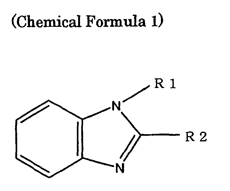
- The photoelectric transducer according to claim 1, wherein the electrolyte layer contains a room temperature molten salt.
- The photoelectric transducer according to claim 4, wherein the room temperature molten salt is 1-methyl-3-propylimidazolium iodide.
- The photoelectric transducer according to claim 1, wherein the electrolyte layer contains a nitrile solvent having a boiling point of 100°C or higher.
- The photoelectric transducer according to claim 6, wherein the nitrile solvent is 3-methoxypropionitrile.
- A photoelectric transducer comprising: a semiconductor electrode provided with a semiconductor layer supporting a sensitizing dye; a counter electrode opposed to the semiconductor electrode; and an electrolyte layer interposed between the semiconductor electrode and the counter electrode,
wherein the electrolyte layer includes a polymer compound as a matrix and a compound containing a nitrogen atom having non-shared electron pairs in a molecule. - The photoelectric transducer according to claim 8, wherein the polymer compound is a vinylidene fluoride polymer.
- The photoelectric transducer according to claim 8, wherein the electrolyte layer contains iodine (I3 -) with a concentration of 0.06 mol/dm3 to 6 mol/dm3.
- The photoelectric transducer according to claim 8, wherein a concentration of the compound containing a nitrogen atom having non-shared electron pairs in a molecule in the electrolyte layer is in a range of 5 × 10⁻⁴ mol/dm3 to 2 mol/dm3.
- The photoelectric transducer according to claim 8, wherein the compound containing a nitrogen atom having non-shared electron pairs in a molecule is represented by the following Chemical Formula 2 (where R1 and R2 respectively are any substituents selected from the group consisting of an alkyl group, an alkoxyl group, an alkenyl group, an alkynyl group, an alkoxylalkyl group, a polyether group, and a phenyl group (any of the substituents includes 1 to 20 carbon atoms and may be linear or branched, and another element may substitute for a part or an entire of hydrogen) or hydrogen, and R1 and R2 may be different from each other).

- The photoelectric transducer according to claim 8, wherein the electrolyte layer contains a room temperature molten salt.
- The photoelectric transducer according to claim 13, wherein the room temperature molten salt is 1-methyl-3-propylimidazolium iodide.
- The photoelectric transducer according to claim 8, wherein the electrolyte layer contains a nitrile solvent having a boiling point of 100°C or higher.
- The photoelectric transducer according to claim 15, wherein the nitrile solvent is 3-methoxypropionitrile.
Applications Claiming Priority (3)
| Application Number | Priority Date | Filing Date | Title |
|---|---|---|---|
| JP2002145358 | 2002-05-20 | ||
| JP2002145358 | 2002-05-20 | ||
| PCT/JP2003/005426 WO2003098731A1 (en) | 2002-05-20 | 2003-04-28 | Photoelectric conversion device |
Related Child Applications (1)
| Application Number | Title | Priority Date | Filing Date |
|---|---|---|---|
| EP07107824 Division | 2003-04-28 |
Publications (4)
| Publication Number | Publication Date |
|---|---|
| EP1507307A1 true EP1507307A1 (en) | 2005-02-16 |
| EP1507307A4 EP1507307A4 (en) | 2005-04-20 |
| EP1507307B1 EP1507307B1 (en) | 2008-03-05 |
| EP1507307B9 EP1507307B9 (en) | 2008-08-13 |
Family
ID=29545086
Family Applications (1)
| Application Number | Title | Priority Date | Filing Date |
|---|---|---|---|
| EP03725689A Expired - Lifetime EP1507307B9 (en) | 2002-05-20 | 2003-04-28 | Photoelectric conversion device |
Country Status (9)
| Country | Link |
|---|---|
| US (1) | US20040238826A1 (en) |
| EP (1) | EP1507307B9 (en) |
| JP (1) | JP4185490B2 (en) |
| CN (1) | CN1322592C (en) |
| AT (1) | ATE388475T1 (en) |
| AU (1) | AU2003231536B2 (en) |
| DE (1) | DE60319522T2 (en) |
| ES (1) | ES2304508T3 (en) |
| WO (1) | WO2003098731A1 (en) |
Cited By (20)
| Publication number | Priority date | Publication date | Assignee | Title |
|---|---|---|---|---|
| WO2007093961A1 (en) | 2006-02-13 | 2007-08-23 | Ecole Polytechnique Federale De Lausanne (Epfl) | Ionic liquid electrolyte |
| EP2301932A1 (en) | 2009-09-29 | 2011-03-30 | Ecole Polytechnique Fédérale de Lausanne (EPFL) | Novel ligands for sensitizing dyes of dye-sensitized solar cells |
| EP2325913A1 (en) | 2006-03-23 | 2011-05-25 | Ecole Polytechnique Fédérale de Lausanne (EPFL) | A method for preparing a solar cell |
| WO2011085967A1 (en) | 2010-01-18 | 2011-07-21 | Merck Patent Gmbh | Compounds containing perfluoroalkyl-cyano-alkoxy-borate anions or perfluoroalkyl-cyano-alkoxy-fluoro-borate anions |
| WO2011085964A1 (en) | 2010-01-18 | 2011-07-21 | Merck Patent Gmbh | Electrolyte formulations |
| WO2011085965A1 (en) | 2010-01-18 | 2011-07-21 | Merck Patent Gmbh | Electrolyte formulations |
| WO2011125024A1 (en) | 2010-04-05 | 2011-10-13 | Ecole Polytechnique Federale De Lausanne (Epfl) | Improved electrode |
| EP2388853A1 (en) | 2010-05-20 | 2011-11-23 | Fundacion Cidetec | Ionic liquid based electrolytes containing sulfide/polysulfide redox couple and uses thereof |
| WO2011144306A1 (en) | 2010-05-17 | 2011-11-24 | Daunia Solar Cell S.R.L. | New gel electrolytes suitable for photoelectrochemical devices |
| WO2012041437A2 (en) | 2010-09-30 | 2012-04-05 | Merck Patent Gmbh | Electrolyte formulations |
| WO2012048772A1 (en) | 2010-09-27 | 2012-04-19 | Merck Patent Gmbh | Functionalized fluoroalkyl fluorophosphate salts |
| WO2012076093A1 (en) | 2010-12-08 | 2012-06-14 | Merck Patent Gmbh | Additives for dye-sensitized solar cells |
| WO2012163490A1 (en) | 2011-05-31 | 2012-12-06 | Merck Patent Gmbh | Electrolyte formulations |
| WO2013010640A1 (en) | 2011-07-15 | 2013-01-24 | Merck Patent Gmbh | Compounds containing alkyl-alkoxy-cyano-borate anions |
| WO2013010641A1 (en) | 2011-07-15 | 2013-01-24 | Merck Patent Gmbh | Compounds containing alkyl-cyano-borate or alkyl-cyano-fluoroborate anions |
| WO2013026563A1 (en) | 2011-08-25 | 2013-02-28 | Merck Patent Gmbh | Additives for dye-sensitized solar cells |
| WO2013057538A1 (en) | 2011-10-18 | 2013-04-25 | École Polytechnique Fédérale De Lausanne (Epfl) | Compounds for electrochemical and/or optoelectronic devices |
| WO2013084029A1 (en) | 2011-12-08 | 2013-06-13 | Ecole Polytechnique Federale De Lausanne (Epfl) | Semiconductor electrode comprising a blocking layer |
| EP2883881A1 (en) | 2013-12-12 | 2015-06-17 | Merck Patent GmbH | Cobaltcomplex salts and mixtures of Cobaltcomplex salts for use in DSSC |
| DE102013021029A1 (en) | 2013-12-17 | 2015-07-02 | Julius-Maximilians-Universität Würzburg | Cobalt complex salts |
Families Citing this family (25)
| Publication number | Priority date | Publication date | Assignee | Title |
|---|---|---|---|---|
| US8444834B2 (en) | 1999-11-15 | 2013-05-21 | Abbott Diabetes Care Inc. | Redox polymers for use in analyte monitoring |
| EP1230249B1 (en) | 1999-11-15 | 2004-06-02 | Therasense, Inc. | Transition metal complexes with bidentate ligand having an imidazole ring |
| US8268143B2 (en) | 1999-11-15 | 2012-09-18 | Abbott Diabetes Care Inc. | Oxygen-effect free analyte sensor |
| US8070934B2 (en) | 2001-05-11 | 2011-12-06 | Abbott Diabetes Care Inc. | Transition metal complexes with (pyridyl)imidazole ligands |
| US6676816B2 (en) | 2001-05-11 | 2004-01-13 | Therasense, Inc. | Transition metal complexes with (pyridyl)imidazole ligands and sensors using said complexes |
| US8226814B2 (en) | 2001-05-11 | 2012-07-24 | Abbott Diabetes Care Inc. | Transition metal complexes with pyridyl-imidazole ligands |
| AU2006234481A1 (en) * | 2005-04-11 | 2006-10-19 | Nippon Kayaku Kabushiki Kaisha | Electrolyte composition for photoelectric converter and photoelectric converter using same |
| DE102005060392A1 (en) | 2005-12-16 | 2007-06-21 | Süd-Chemie AG | Separating proteins from liquid media, useful e.g. for isolation of proteins from bioreactors or body fluids, using specific clay material that does not swell much in water |
| KR100844871B1 (en) * | 2007-04-06 | 2008-07-09 | 경북대학교 산학협력단 | A dye for dye-sensitized solar cell and solar cell using it |
| JP5209344B2 (en) * | 2007-05-17 | 2013-06-12 | 大同メタル工業株式会社 | Dye-sensitized solar cell preparation kit, dye-sensitized solar cell and method of using the same |
| DE102008023454A1 (en) | 2007-05-17 | 2008-11-27 | Daido Metal Co. Ltd., Nagoya | Kit for the production of color-sensitized solar cells, color-sensitized solar process and use thereof |
| WO2010029943A1 (en) * | 2008-09-10 | 2010-03-18 | パナソニック電工株式会社 | Radio identification card |
| US8338692B2 (en) * | 2008-11-27 | 2012-12-25 | The Yokohama Rubber Co., Ltd. | Electrolyte for photoelectric conversion elements, and photoelectric conversion element and dye-sensitized solar cell using the electrolyte |
| JP4557097B2 (en) * | 2008-11-27 | 2010-10-06 | 横浜ゴム株式会社 | Electrolyte for photoelectric conversion element and photoelectric conversion element and dye-sensitized solar cell using the electrolyte |
| WO2010074237A1 (en) * | 2008-12-26 | 2010-07-01 | 横浜ゴム株式会社 | Electrolyte for photoelectric conversion element, and photoelectric conversion element and dye-sensitized solar cell each utilizing the electrolyte |
| CN101819838B (en) * | 2010-03-02 | 2012-10-03 | 中国科学院上海应用物理研究所 | Alkynyl-modified magnetic nano-particle module, amino acid compound-modified magnetic nano-particles, preparation method and application thereof |
| CN101777428B (en) * | 2010-03-15 | 2012-05-23 | 彩虹集团公司 | Method for preparing counter electrode of dye-sensitized solar cell |
| CN101777430B (en) * | 2010-03-15 | 2012-07-04 | 彩虹集团公司 | Preparation method for titanium dioxide membrane used as dye-sensitized solar cell photo-anode |
| JP5773837B2 (en) * | 2011-10-20 | 2015-09-02 | 大阪瓦斯株式会社 | Electrolytic solution and photoelectric conversion element |
| WO2014008396A1 (en) * | 2012-07-03 | 2014-01-09 | Massachusetts Institute Technology | Virus film as template for porous inorganic scaffolds |
| CN103903859A (en) * | 2012-12-27 | 2014-07-02 | 中国科学院上海硅酸盐研究所 | Method for preparing photoanode of dye-sensitized solar cell through coating |
| CN104201362A (en) * | 2014-05-04 | 2014-12-10 | 昆明理工大学 | Preparing method of carbon-doped titanium oxide nanotube array lithium battery anode material |
| JP2019117889A (en) * | 2017-12-27 | 2019-07-18 | 太陽誘電株式会社 | Dye-sensitized solar cell |
| CN108479806B (en) * | 2018-01-06 | 2020-04-28 | 中南大学 | Heterojunction film composed of same metal and oxygen group element, preparation and application thereof |
| CA3106260A1 (en) * | 2018-09-21 | 2020-03-26 | Ambient Photonics, Inc. | Dye-sensitized photovoltaic cells |
Citations (2)
| Publication number | Priority date | Publication date | Assignee | Title |
|---|---|---|---|---|
| EP0986079A2 (en) * | 1998-09-09 | 2000-03-15 | Fuji Photo Film Co., Ltd. | Photo-electrochemical cell |
| EP1180774A2 (en) * | 2000-08-15 | 2002-02-20 | Fuji Photo Film Co., Ltd. | Photoelectric conversion device and method for producing same |
Family Cites Families (11)
| Publication number | Priority date | Publication date | Assignee | Title |
|---|---|---|---|---|
| CH674596A5 (en) * | 1988-02-12 | 1990-06-15 | Sulzer Ag | |
| US5728487A (en) * | 1993-12-29 | 1998-03-17 | Ecole Polytechnique Federale De Lausanne | Photoelectrochemical cell and electrolyte for this cell |
| ES2244958T3 (en) * | 1994-12-21 | 2005-12-16 | Hydro Quebec | LIQUID HYDROPHOBIC SALTS, ITS PREPRATION AND ITS APPLICATION IN ELECTROCHEMISTRY. |
| JPH11144773A (en) * | 1997-09-05 | 1999-05-28 | Fuji Photo Film Co Ltd | Photoelectric converting element and light regenerating type photoelectric chemical battery |
| JP4111360B2 (en) * | 1998-08-11 | 2008-07-02 | 富士フイルム株式会社 | Gel electrolyte, gel electrolyte for photoelectrochemical cell, and photoelectrochemical cell |
| JP2000058891A (en) * | 1998-08-11 | 2000-02-25 | Fuji Photo Film Co Ltd | Electrolyte, electrolyte for photoelectric chemical cell, photoelectric chemical battery and pyridinium compound |
| JP3462115B2 (en) * | 1999-03-29 | 2003-11-05 | 三洋化成工業株式会社 | Non-aqueous electrolyte for dye-sensitized solar cell and solar cell using the same |
| US6291763B1 (en) * | 1999-04-06 | 2001-09-18 | Fuji Photo Film Co., Ltd. | Photoelectric conversion device and photo cell |
| US6900382B2 (en) * | 2002-01-25 | 2005-05-31 | Konarka Technologies, Inc. | Gel electrolytes for dye sensitized solar cells |
| JP4222466B2 (en) * | 2001-06-14 | 2009-02-12 | 富士フイルム株式会社 | Charge transport material, photoelectric conversion element and photovoltaic cell using the same, and pyridine compound |
| JP4021637B2 (en) * | 2001-09-27 | 2007-12-12 | 株式会社東芝 | Photosensitized solar cell and method for producing the same |
-
2003
- 2003-04-28 US US10/487,751 patent/US20040238826A1/en not_active Abandoned
- 2003-04-28 WO PCT/JP2003/005426 patent/WO2003098731A1/en active IP Right Grant
- 2003-04-28 JP JP2004506116A patent/JP4185490B2/en not_active Expired - Fee Related
- 2003-04-28 ES ES03725689T patent/ES2304508T3/en not_active Expired - Lifetime
- 2003-04-28 AT AT03725689T patent/ATE388475T1/en not_active IP Right Cessation
- 2003-04-28 AU AU2003231536A patent/AU2003231536B2/en not_active Ceased
- 2003-04-28 EP EP03725689A patent/EP1507307B9/en not_active Expired - Lifetime
- 2003-04-28 CN CN03801649.4A patent/CN1322592C/en not_active Expired - Fee Related
- 2003-04-28 DE DE60319522T patent/DE60319522T2/en not_active Expired - Lifetime
Patent Citations (2)
| Publication number | Priority date | Publication date | Assignee | Title |
|---|---|---|---|---|
| EP0986079A2 (en) * | 1998-09-09 | 2000-03-15 | Fuji Photo Film Co., Ltd. | Photo-electrochemical cell |
| EP1180774A2 (en) * | 2000-08-15 | 2002-02-20 | Fuji Photo Film Co., Ltd. | Photoelectric conversion device and method for producing same |
Non-Patent Citations (5)
| Title |
|---|
| A. HINSCH ET AL.: "Long-term Stability of Dye-Sensitized Solar Cells" PROG. PHOTOVOLT: RES. APPL., vol. 9, pages 425-438, * |
| G. BOSVHLOO, H. LINDSTRÖM, E. MAGNUSSON, A. HOLMBERG, A. HAGFELDT: "Optimization of dye sensitized solar cells prepared by compression method" J. PHOTOCHEM. PHOTOBIOL. A: CHEM., vol. 148, 18 March 2002 (2002-03-18), pages 11-15, XP008043909 * |
| K. KAWATA, S. M. ZAKEERUDDIN, M. GRÄTZEL: "Solvent Free Dye-Sensitized Nanocrystalline Solar Cell Using Room-Temperature Molten Salt Electrolyte" ELECTROCHEMICAL SOCIETY PROCEEDINGS, vol. 2002-19, 12 May 2002 (2002-05-12), - 17 May 2002 (2002-05-17) pages 16-30, XP008029687 * |
| N.PAPAGEORGIOU ET AL.: "The Performance and Stability of Ambient Temperature Molten Salts for SOlar Cell Applications" J. ELECTROCHEM. SOC., vol. 143, no. 10, 1996, pages 3099-3108, XP002118482 * |
| See also references of WO03098731A1 * |
Cited By (25)
| Publication number | Priority date | Publication date | Assignee | Title |
|---|---|---|---|---|
| WO2007093961A1 (en) | 2006-02-13 | 2007-08-23 | Ecole Polytechnique Federale De Lausanne (Epfl) | Ionic liquid electrolyte |
| EP2325913A1 (en) | 2006-03-23 | 2011-05-25 | Ecole Polytechnique Fédérale de Lausanne (EPFL) | A method for preparing a solar cell |
| EP2301932A1 (en) | 2009-09-29 | 2011-03-30 | Ecole Polytechnique Fédérale de Lausanne (EPFL) | Novel ligands for sensitizing dyes of dye-sensitized solar cells |
| WO2011039715A1 (en) | 2009-09-29 | 2011-04-07 | Ecole Polytechnique Federale De Lausanne (Epfl) | Novel ligands for sensitizing dyes of dye-sensitized solar cells |
| WO2011085965A1 (en) | 2010-01-18 | 2011-07-21 | Merck Patent Gmbh | Electrolyte formulations |
| WO2011085964A1 (en) | 2010-01-18 | 2011-07-21 | Merck Patent Gmbh | Electrolyte formulations |
| US8835667B2 (en) | 2010-01-18 | 2014-09-16 | Merck Patent Gmbh | Electrolyte formulations |
| WO2011085967A1 (en) | 2010-01-18 | 2011-07-21 | Merck Patent Gmbh | Compounds containing perfluoroalkyl-cyano-alkoxy-borate anions or perfluoroalkyl-cyano-alkoxy-fluoro-borate anions |
| US8901340B2 (en) | 2010-01-18 | 2014-12-02 | Merck Patent Gmbh | Compounds containing perfluoroalkyl-cyano-alkoxy-borate anions or perfluoroalkyl-cyano-alkoxy-fluoro-borate anions |
| WO2011125024A1 (en) | 2010-04-05 | 2011-10-13 | Ecole Polytechnique Federale De Lausanne (Epfl) | Improved electrode |
| WO2011144306A1 (en) | 2010-05-17 | 2011-11-24 | Daunia Solar Cell S.R.L. | New gel electrolytes suitable for photoelectrochemical devices |
| WO2011145120A1 (en) | 2010-05-17 | 2011-11-24 | Daunia Solar Cell S.R.L. | New gel electrolytes suitable for photoelectrochemical devices |
| EP2388853A1 (en) | 2010-05-20 | 2011-11-23 | Fundacion Cidetec | Ionic liquid based electrolytes containing sulfide/polysulfide redox couple and uses thereof |
| WO2011144697A1 (en) | 2010-05-20 | 2011-11-24 | Fundacion Cidetec | Ionic liquid based electrolytes containing sulfide/polysulfide redox couple and uses thereof |
| WO2012048772A1 (en) | 2010-09-27 | 2012-04-19 | Merck Patent Gmbh | Functionalized fluoroalkyl fluorophosphate salts |
| WO2012041437A2 (en) | 2010-09-30 | 2012-04-05 | Merck Patent Gmbh | Electrolyte formulations |
| WO2012076093A1 (en) | 2010-12-08 | 2012-06-14 | Merck Patent Gmbh | Additives for dye-sensitized solar cells |
| WO2012163490A1 (en) | 2011-05-31 | 2012-12-06 | Merck Patent Gmbh | Electrolyte formulations |
| WO2013010640A1 (en) | 2011-07-15 | 2013-01-24 | Merck Patent Gmbh | Compounds containing alkyl-alkoxy-cyano-borate anions |
| WO2013010641A1 (en) | 2011-07-15 | 2013-01-24 | Merck Patent Gmbh | Compounds containing alkyl-cyano-borate or alkyl-cyano-fluoroborate anions |
| WO2013026563A1 (en) | 2011-08-25 | 2013-02-28 | Merck Patent Gmbh | Additives for dye-sensitized solar cells |
| WO2013057538A1 (en) | 2011-10-18 | 2013-04-25 | École Polytechnique Fédérale De Lausanne (Epfl) | Compounds for electrochemical and/or optoelectronic devices |
| WO2013084029A1 (en) | 2011-12-08 | 2013-06-13 | Ecole Polytechnique Federale De Lausanne (Epfl) | Semiconductor electrode comprising a blocking layer |
| EP2883881A1 (en) | 2013-12-12 | 2015-06-17 | Merck Patent GmbH | Cobaltcomplex salts and mixtures of Cobaltcomplex salts for use in DSSC |
| DE102013021029A1 (en) | 2013-12-17 | 2015-07-02 | Julius-Maximilians-Universität Würzburg | Cobalt complex salts |
Also Published As
| Publication number | Publication date |
|---|---|
| ES2304508T3 (en) | 2008-10-16 |
| AU2003231536B2 (en) | 2006-01-12 |
| WO2003098731A1 (en) | 2003-11-27 |
| ATE388475T1 (en) | 2008-03-15 |
| AU2003231536A1 (en) | 2003-12-02 |
| DE60319522D1 (en) | 2008-04-17 |
| JP4185490B2 (en) | 2008-11-26 |
| JPWO2003098731A1 (en) | 2005-09-22 |
| CN1596484A (en) | 2005-03-16 |
| EP1507307B9 (en) | 2008-08-13 |
| EP1507307A4 (en) | 2005-04-20 |
| US20040238826A1 (en) | 2004-12-02 |
| DE60319522T2 (en) | 2009-04-02 |
| CN1322592C (en) | 2007-06-20 |
| EP1507307B1 (en) | 2008-03-05 |
Similar Documents
| Publication | Publication Date | Title |
|---|---|---|
| AU2003231536B2 (en) | Photoelectric conversion device | |
| JP4415448B2 (en) | Photoelectric conversion element | |
| US6683361B2 (en) | Solar cell and solar cell unit | |
| JP4415481B2 (en) | Photoelectric conversion element and manufacturing method thereof | |
| JP5237664B2 (en) | Photoelectric conversion element | |
| JP2002170602A (en) | Photoelectric conversion element | |
| JP4696452B2 (en) | Photoelectric conversion element | |
| JP4479108B2 (en) | Photoelectric conversion element | |
| JP4423735B2 (en) | Photoelectric conversion element | |
| JP4415482B2 (en) | Photoelectric conversion element | |
| JP4135323B2 (en) | Method for manufacturing photoelectric conversion element | |
| JP4341197B2 (en) | Photoelectric conversion element and manufacturing method thereof | |
| JP2003187883A (en) | Photoelectric conversion element | |
| JP5584447B2 (en) | Photoelectric element | |
| JP4320869B2 (en) | Method for manufacturing photoelectric conversion element | |
| JP4092908B2 (en) | Photoelectric conversion element and manufacturing method thereof | |
| JP2008186632A (en) | Photoelectric conversion element and its manufacturing method | |
| JP2002313445A (en) | Photoelectric transducer | |
| JP5181507B2 (en) | Method for manufacturing photoelectric conversion element | |
| JP4352552B2 (en) | Photoelectric conversion element and photovoltaic cell | |
| JP6415380B2 (en) | Photoelectric conversion element | |
| JP2001273938A (en) | Photoelectric transducer | |
| JP2008243623A (en) | Manufacturing method of photoelectric conversion element, and photoelectric conversion element | |
| JP2008052936A (en) | Photoelectric conversion element |
Legal Events
| Date | Code | Title | Description |
|---|---|---|---|
| PUAI | Public reference made under article 153(3) epc to a published international application that has entered the european phase |
Free format text: ORIGINAL CODE: 0009012 |
|
| 17P | Request for examination filed |
Effective date: 20040416 |
|
| AK | Designated contracting states |
Kind code of ref document: A1 Designated state(s): AT BE BG CH CY CZ DE DK EE ES FI FR GB GR HU IE IT LI LU MC NL PT RO SE SI SK TR |
|
| AX | Request for extension of the european patent |
Extension state: AL LT LV MK |
|
| A4 | Supplementary search report drawn up and despatched |
Effective date: 20050309 |
|
| RIC1 | Information provided on ipc code assigned before grant |
Ipc: 7H 01G 9/20 A |
|
| DAX | Request for extension of the european patent (deleted) | ||
| GRAP | Despatch of communication of intention to grant a patent |
Free format text: ORIGINAL CODE: EPIDOSNIGR1 |
|
| GRAS | Grant fee paid |
Free format text: ORIGINAL CODE: EPIDOSNIGR3 |
|
| RAP1 | Party data changed (applicant data changed or rights of an application transferred) |
Owner name: ECOLE POLYTECHNIQUE FEDERALE DE LAUSANNE (EPFL) Owner name: MATSUSHITA ELECTRIC WORKS, LTD. |
|
| GRAA | (expected) grant |
Free format text: ORIGINAL CODE: 0009210 |
|
| AK | Designated contracting states |
Kind code of ref document: B1 Designated state(s): AT BE BG CH CY CZ DE DK EE ES FI FR GB GR HU IE IT LI LU MC NL PT RO SE SI SK TR |
|
| REG | Reference to a national code |
Ref country code: GB Ref legal event code: FG4D |
|
| REG | Reference to a national code |
Ref country code: CH Ref legal event code: EP |
|
| REG | Reference to a national code |
Ref country code: IE Ref legal event code: FG4D |
|
| REF | Corresponds to: |
Ref document number: 60319522 Country of ref document: DE Date of ref document: 20080417 Kind code of ref document: P |
|
| REG | Reference to a national code |
Ref country code: GR Ref legal event code: EP Ref document number: 20080401187 Country of ref document: GR |
|
| PG25 | Lapsed in a contracting state [announced via postgrant information from national office to epo] |
Ref country code: FI Free format text: LAPSE BECAUSE OF FAILURE TO SUBMIT A TRANSLATION OF THE DESCRIPTION OR TO PAY THE FEE WITHIN THE PRESCRIBED TIME-LIMIT Effective date: 20080305 |
|
| REG | Reference to a national code |
Ref country code: CH Ref legal event code: NV Representative=s name: ABREMA AGENCE BREVET ET MARQUES, GANGUILLET |
|
| PG25 | Lapsed in a contracting state [announced via postgrant information from national office to epo] |
Ref country code: AT Free format text: LAPSE BECAUSE OF FAILURE TO SUBMIT A TRANSLATION OF THE DESCRIPTION OR TO PAY THE FEE WITHIN THE PRESCRIBED TIME-LIMIT Effective date: 20080305 |
|
| NLV1 | Nl: lapsed or annulled due to failure to fulfill the requirements of art. 29p and 29m of the patents act | ||
| PG25 | Lapsed in a contracting state [announced via postgrant information from national office to epo] |
Ref country code: BE Free format text: LAPSE BECAUSE OF FAILURE TO SUBMIT A TRANSLATION OF THE DESCRIPTION OR TO PAY THE FEE WITHIN THE PRESCRIBED TIME-LIMIT Effective date: 20080305 Ref country code: SI Free format text: LAPSE BECAUSE OF FAILURE TO SUBMIT A TRANSLATION OF THE DESCRIPTION OR TO PAY THE FEE WITHIN THE PRESCRIBED TIME-LIMIT Effective date: 20080305 |
|
| REG | Reference to a national code |
Ref country code: ES Ref legal event code: FG2A Ref document number: 2304508 Country of ref document: ES Kind code of ref document: T3 |
|
| PG25 | Lapsed in a contracting state [announced via postgrant information from national office to epo] |
Ref country code: CZ Free format text: LAPSE BECAUSE OF FAILURE TO SUBMIT A TRANSLATION OF THE DESCRIPTION OR TO PAY THE FEE WITHIN THE PRESCRIBED TIME-LIMIT Effective date: 20080305 Ref country code: NL Free format text: LAPSE BECAUSE OF FAILURE TO SUBMIT A TRANSLATION OF THE DESCRIPTION OR TO PAY THE FEE WITHIN THE PRESCRIBED TIME-LIMIT Effective date: 20080305 Ref country code: PT Free format text: LAPSE BECAUSE OF FAILURE TO SUBMIT A TRANSLATION OF THE DESCRIPTION OR TO PAY THE FEE WITHIN THE PRESCRIBED TIME-LIMIT Effective date: 20080805 Ref country code: SK Free format text: LAPSE BECAUSE OF FAILURE TO SUBMIT A TRANSLATION OF THE DESCRIPTION OR TO PAY THE FEE WITHIN THE PRESCRIBED TIME-LIMIT Effective date: 20080305 Ref country code: SE Free format text: LAPSE BECAUSE OF FAILURE TO SUBMIT A TRANSLATION OF THE DESCRIPTION OR TO PAY THE FEE WITHIN THE PRESCRIBED TIME-LIMIT Effective date: 20080605 |
|
| ET | Fr: translation filed | ||
| PG25 | Lapsed in a contracting state [announced via postgrant information from national office to epo] |
Ref country code: MC Free format text: LAPSE BECAUSE OF NON-PAYMENT OF DUE FEES Effective date: 20080430 Ref country code: RO Free format text: LAPSE BECAUSE OF FAILURE TO SUBMIT A TRANSLATION OF THE DESCRIPTION OR TO PAY THE FEE WITHIN THE PRESCRIBED TIME-LIMIT Effective date: 20080305 |
|
| PLBE | No opposition filed within time limit |
Free format text: ORIGINAL CODE: 0009261 |
|
| STAA | Information on the status of an ep patent application or granted ep patent |
Free format text: STATUS: NO OPPOSITION FILED WITHIN TIME LIMIT |
|
| PG25 | Lapsed in a contracting state [announced via postgrant information from national office to epo] |
Ref country code: EE Free format text: LAPSE BECAUSE OF FAILURE TO SUBMIT A TRANSLATION OF THE DESCRIPTION OR TO PAY THE FEE WITHIN THE PRESCRIBED TIME-LIMIT Effective date: 20080305 Ref country code: DK Free format text: LAPSE BECAUSE OF FAILURE TO SUBMIT A TRANSLATION OF THE DESCRIPTION OR TO PAY THE FEE WITHIN THE PRESCRIBED TIME-LIMIT Effective date: 20080305 |
|
| 26N | No opposition filed |
Effective date: 20081208 |
|
| PG25 | Lapsed in a contracting state [announced via postgrant information from national office to epo] |
Ref country code: IE Free format text: LAPSE BECAUSE OF NON-PAYMENT OF DUE FEES Effective date: 20080428 Ref country code: BG Free format text: LAPSE BECAUSE OF FAILURE TO SUBMIT A TRANSLATION OF THE DESCRIPTION OR TO PAY THE FEE WITHIN THE PRESCRIBED TIME-LIMIT Effective date: 20080605 |
|
| PG25 | Lapsed in a contracting state [announced via postgrant information from national office to epo] |
Ref country code: CY Free format text: LAPSE BECAUSE OF FAILURE TO SUBMIT A TRANSLATION OF THE DESCRIPTION OR TO PAY THE FEE WITHIN THE PRESCRIBED TIME-LIMIT Effective date: 20080305 |
|
| PG25 | Lapsed in a contracting state [announced via postgrant information from national office to epo] |
Ref country code: LU Free format text: LAPSE BECAUSE OF NON-PAYMENT OF DUE FEES Effective date: 20080428 Ref country code: HU Free format text: LAPSE BECAUSE OF FAILURE TO SUBMIT A TRANSLATION OF THE DESCRIPTION OR TO PAY THE FEE WITHIN THE PRESCRIBED TIME-LIMIT Effective date: 20080906 |
|
| PG25 | Lapsed in a contracting state [announced via postgrant information from national office to epo] |
Ref country code: TR Free format text: LAPSE BECAUSE OF FAILURE TO SUBMIT A TRANSLATION OF THE DESCRIPTION OR TO PAY THE FEE WITHIN THE PRESCRIBED TIME-LIMIT Effective date: 20080305 |
|
| PGFP | Annual fee paid to national office [announced via postgrant information from national office to epo] |
Ref country code: ES Payment date: 20120425 Year of fee payment: 10 |
|
| PGFP | Annual fee paid to national office [announced via postgrant information from national office to epo] |
Ref country code: GR Payment date: 20130419 Year of fee payment: 11 Ref country code: IT Payment date: 20130429 Year of fee payment: 11 |
|
| REG | Reference to a national code |
Ref country code: GR Ref legal event code: ML Ref document number: 20080401187 Country of ref document: GR Effective date: 20141104 |
|
| PG25 | Lapsed in a contracting state [announced via postgrant information from national office to epo] |
Ref country code: GR Free format text: LAPSE BECAUSE OF NON-PAYMENT OF DUE FEES Effective date: 20141104 |
|
| PG25 | Lapsed in a contracting state [announced via postgrant information from national office to epo] |
Ref country code: IT Free format text: LAPSE BECAUSE OF NON-PAYMENT OF DUE FEES Effective date: 20140428 |
|
| REG | Reference to a national code |
Ref country code: FR Ref legal event code: PLFP Year of fee payment: 13 |
|
| REG | Reference to a national code |
Ref country code: ES Ref legal event code: FD2A Effective date: 20150528 |
|
| PG25 | Lapsed in a contracting state [announced via postgrant information from national office to epo] |
Ref country code: ES Free format text: LAPSE BECAUSE OF NON-PAYMENT OF DUE FEES Effective date: 20140429 |
|
| PGFP | Annual fee paid to national office [announced via postgrant information from national office to epo] |
Ref country code: CH Payment date: 20150504 Year of fee payment: 13 Ref country code: DE Payment date: 20150421 Year of fee payment: 13 Ref country code: GB Payment date: 20150420 Year of fee payment: 13 |
|
| PGFP | Annual fee paid to national office [announced via postgrant information from national office to epo] |
Ref country code: FR Payment date: 20150421 Year of fee payment: 13 |
|
| REG | Reference to a national code |
Ref country code: DE Ref legal event code: R119 Ref document number: 60319522 Country of ref document: DE |
|
| REG | Reference to a national code |
Ref country code: CH Ref legal event code: PL |
|
| GBPC | Gb: european patent ceased through non-payment of renewal fee |
Effective date: 20160428 |
|
| REG | Reference to a national code |
Ref country code: FR Ref legal event code: ST Effective date: 20161230 |
|
| PG25 | Lapsed in a contracting state [announced via postgrant information from national office to epo] |
Ref country code: CH Free format text: LAPSE BECAUSE OF NON-PAYMENT OF DUE FEES Effective date: 20160430 Ref country code: DE Free format text: LAPSE BECAUSE OF NON-PAYMENT OF DUE FEES Effective date: 20161101 Ref country code: GB Free format text: LAPSE BECAUSE OF NON-PAYMENT OF DUE FEES Effective date: 20160428 Ref country code: LI Free format text: LAPSE BECAUSE OF NON-PAYMENT OF DUE FEES Effective date: 20160430 Ref country code: FR Free format text: LAPSE BECAUSE OF NON-PAYMENT OF DUE FEES Effective date: 20160502 |