EP1505661A2 - GaN-based LED and its manufacturing method - Google Patents
GaN-based LED and its manufacturing method Download PDFInfo
- Publication number
- EP1505661A2 EP1505661A2 EP04018710A EP04018710A EP1505661A2 EP 1505661 A2 EP1505661 A2 EP 1505661A2 EP 04018710 A EP04018710 A EP 04018710A EP 04018710 A EP04018710 A EP 04018710A EP 1505661 A2 EP1505661 A2 EP 1505661A2
- Authority
- EP
- European Patent Office
- Prior art keywords
- substrate
- gan
- light generating
- based semiconductor
- light
- Prior art date
- Legal status (The legal status is an assumption and is not a legal conclusion. Google has not performed a legal analysis and makes no representation as to the accuracy of the status listed.)
- Withdrawn
Links
- 238000004519 manufacturing process Methods 0.000 title claims abstract description 20
- 239000004065 semiconductor Substances 0.000 claims abstract description 188
- 239000000758 substrate Substances 0.000 claims abstract description 177
- 239000000853 adhesive Substances 0.000 claims abstract description 14
- 230000001070 adhesive effect Effects 0.000 claims abstract description 14
- 238000000034 method Methods 0.000 claims description 64
- JMASRVWKEDWRBT-UHFFFAOYSA-N Gallium nitride Chemical compound [Ga]#N JMASRVWKEDWRBT-UHFFFAOYSA-N 0.000 claims description 51
- 239000000463 material Substances 0.000 claims description 38
- 229910001080 W alloy Inorganic materials 0.000 claims description 18
- 238000002310 reflectometry Methods 0.000 claims description 12
- 229910000679 solder Inorganic materials 0.000 claims description 12
- 229910015363 Au—Sn Inorganic materials 0.000 claims description 10
- 229910052782 aluminium Inorganic materials 0.000 claims description 8
- XAGFODPZIPBFFR-UHFFFAOYSA-N aluminium Chemical compound [Al] XAGFODPZIPBFFR-UHFFFAOYSA-N 0.000 claims description 8
- -1 nitride compound Chemical class 0.000 claims description 7
- 229910052738 indium Inorganic materials 0.000 claims description 6
- APFVFJFRJDLVQX-UHFFFAOYSA-N indium atom Chemical compound [In] APFVFJFRJDLVQX-UHFFFAOYSA-N 0.000 claims description 6
- 230000001678 irradiating effect Effects 0.000 claims description 6
- 229910052751 metal Inorganic materials 0.000 claims description 6
- 239000002184 metal Substances 0.000 claims description 6
- 150000004767 nitrides Chemical class 0.000 claims description 5
- 150000001875 compounds Chemical class 0.000 claims description 4
- 229910001030 Iron–nickel alloy Inorganic materials 0.000 claims description 3
- 229910045601 alloy Inorganic materials 0.000 claims description 3
- 239000000956 alloy Substances 0.000 claims description 3
- 229910002704 AlGaN Inorganic materials 0.000 abstract description 76
- 238000002488 metal-organic chemical vapour deposition Methods 0.000 description 15
- QGZKDVFQNNGYKY-UHFFFAOYSA-N Ammonia Chemical compound N QGZKDVFQNNGYKY-UHFFFAOYSA-N 0.000 description 12
- 230000015572 biosynthetic process Effects 0.000 description 11
- 239000000203 mixture Substances 0.000 description 11
- XCZXGTMEAKBVPV-UHFFFAOYSA-N trimethylgallium Chemical compound C[Ga](C)C XCZXGTMEAKBVPV-UHFFFAOYSA-N 0.000 description 11
- 229910000069 nitrogen hydride Inorganic materials 0.000 description 10
- 229910052594 sapphire Inorganic materials 0.000 description 10
- 239000010980 sapphire Substances 0.000 description 10
- 230000003287 optical effect Effects 0.000 description 8
- BLRPTPMANUNPDV-UHFFFAOYSA-N Silane Chemical compound [SiH4] BLRPTPMANUNPDV-UHFFFAOYSA-N 0.000 description 7
- 238000004140 cleaning Methods 0.000 description 6
- 238000002347 injection Methods 0.000 description 6
- 239000007924 injection Substances 0.000 description 6
- 238000010521 absorption reaction Methods 0.000 description 5
- 238000000926 separation method Methods 0.000 description 5
- 238000001465 metallisation Methods 0.000 description 4
- 239000013078 crystal Substances 0.000 description 3
- 230000006798 recombination Effects 0.000 description 3
- 238000005215 recombination Methods 0.000 description 3
- IBEFSUTVZWZJEL-UHFFFAOYSA-N trimethylindium Chemical compound C[In](C)C IBEFSUTVZWZJEL-UHFFFAOYSA-N 0.000 description 3
- 230000003247 decreasing effect Effects 0.000 description 2
- 238000005498 polishing Methods 0.000 description 2
- 239000010948 rhodium Substances 0.000 description 2
- 238000009738 saturating Methods 0.000 description 2
- 239000000243 solution Substances 0.000 description 2
- 229910020220 Pb—Sn Inorganic materials 0.000 description 1
- BQCADISMDOOEFD-UHFFFAOYSA-N Silver Chemical compound [Ag] BQCADISMDOOEFD-UHFFFAOYSA-N 0.000 description 1
- 229910021529 ammonia Inorganic materials 0.000 description 1
- 239000000969 carrier Substances 0.000 description 1
- 239000004020 conductor Substances 0.000 description 1
- 239000000356 contaminant Substances 0.000 description 1
- 238000000151 deposition Methods 0.000 description 1
- 230000008021 deposition Effects 0.000 description 1
- 239000000155 melt Substances 0.000 description 1
- 238000012986 modification Methods 0.000 description 1
- 230000004048 modification Effects 0.000 description 1
- 229910052703 rhodium Inorganic materials 0.000 description 1
- MHOVAHRLVXNVSD-UHFFFAOYSA-N rhodium atom Chemical compound [Rh] MHOVAHRLVXNVSD-UHFFFAOYSA-N 0.000 description 1
- 229910000077 silane Inorganic materials 0.000 description 1
- 229910052709 silver Inorganic materials 0.000 description 1
- 239000004332 silver Substances 0.000 description 1
- 239000000126 substance Substances 0.000 description 1
- 238000001039 wet etching Methods 0.000 description 1
Images







Classifications
-
- H—ELECTRICITY
- H10—SEMICONDUCTOR DEVICES; ELECTRIC SOLID-STATE DEVICES NOT OTHERWISE PROVIDED FOR
- H10H—INORGANIC LIGHT-EMITTING SEMICONDUCTOR DEVICES HAVING POTENTIAL BARRIERS
- H10H20/00—Individual inorganic light-emitting semiconductor devices having potential barriers, e.g. light-emitting diodes [LED]
- H10H20/01—Manufacture or treatment
- H10H20/011—Manufacture or treatment of bodies, e.g. forming semiconductor layers
- H10H20/018—Bonding of wafers
-
- H—ELECTRICITY
- H10—SEMICONDUCTOR DEVICES; ELECTRIC SOLID-STATE DEVICES NOT OTHERWISE PROVIDED FOR
- H10H—INORGANIC LIGHT-EMITTING SEMICONDUCTOR DEVICES HAVING POTENTIAL BARRIERS
- H10H20/00—Individual inorganic light-emitting semiconductor devices having potential barriers, e.g. light-emitting diodes [LED]
- H10H20/01—Manufacture or treatment
- H10H20/011—Manufacture or treatment of bodies, e.g. forming semiconductor layers
- H10H20/013—Manufacture or treatment of bodies, e.g. forming semiconductor layers having light-emitting regions comprising only Group III-V materials
- H10H20/0137—Manufacture or treatment of bodies, e.g. forming semiconductor layers having light-emitting regions comprising only Group III-V materials the light-emitting regions comprising nitride materials
-
- Y—GENERAL TAGGING OF NEW TECHNOLOGICAL DEVELOPMENTS; GENERAL TAGGING OF CROSS-SECTIONAL TECHNOLOGIES SPANNING OVER SEVERAL SECTIONS OF THE IPC; TECHNICAL SUBJECTS COVERED BY FORMER USPC CROSS-REFERENCE ART COLLECTIONS [XRACs] AND DIGESTS
- Y10—TECHNICAL SUBJECTS COVERED BY FORMER USPC
- Y10S—TECHNICAL SUBJECTS COVERED BY FORMER USPC CROSS-REFERENCE ART COLLECTIONS [XRACs] AND DIGESTS
- Y10S438/00—Semiconductor device manufacturing: process
- Y10S438/977—Thinning or removal of substrate
Definitions
- This invention relates to a semiconductor light generating device for the generation of ultraviolet light and so on, and relates to a method of making the ultraviolet light generating semiconductor device.
- Publication 1 Jpn. J. Appl. Phys. Vol. 41 (2002) pp. L1434-1436
- Publication 2 50 th Conference of Japan Society of Applied Physics, Extended Abstract, pp.431
- semiconductor light generating devices include a Cu-W substrate and a semiconductor structure for light emitting diodes (LEDs).
- This light emitting diode semiconductor structure has an active layer of an InGaN multiple quantum structure.
- a Au-Sn layer is formed on the Cu-W substrate.
- the active layer in the light emitting diode semiconductor structure is provided between a p-electrode for p-type semiconductor and an n-electrode for n-type semiconductor.
- the semiconductor light generating devices are fabricated in the following steps.
- a GaN buffer layer and a semiconductor structure for the light emitting diode are sequentially formed on a sapphire substrate by an MOVPE or ELO method.
- the p-electrode is evaporated on one side of the light emitting diode semiconductor structure and the p-electrode is bonded to the Cu-W substrate using Au-Sn solder.
- the sapphire substrate is removed by a laser lift-off (LLO) method using KrF excimer laser, and the remaining GaN buffer layer is removed by polishing it with a chemical mechanical polishing (CMP) method.
- LLO laser lift-off
- CMP chemical mechanical polishing
- the present inventors have found a technical problem on semiconductor light generating devices, such as the light emitting diode (LED). Since the semiconductor light generating devices use a sapphire substrate for making the above semiconductor structure for LEDs, the density of threading dislocations in the active layer is high.
- the semiconductor light generating device in the Publication 1 has the density of threading dislocations, 1.0 ⁇ 10 9 per square centimeters (cm -2 ), and the semiconductor light generating device in the Publication 2 has a relatively low density of threading dislocations, 1.0 ⁇ 10 7 per square centimeters (cm -2 ).
- the threading dislocations reduce the efficiency of light generation in these semiconductor light generating devices.
- AlGaN is available for active layers in these short wavelength light generating devices. Since the efficiency of light generation in the AlGaN light emitting devices is sensitive to threading dislocations in the active layers and the density of threading dislocations in AlGaN semiconductor light generating devices using sapphire substrate is high, these devices do not provide desired light emitting characteristics.
- One aspect of the present invention is a method of making a semiconductor light generating device. This method comprises the steps of: forming a GaN-based semiconductor portion on a Al X Ga 1-X N (0 ⁇ x ⁇ 1) substrate, the GaN-based semiconductor portion including a light generating film; forming an electrode film on the GaN-based semiconductor portion; bonding a conductive substrate to a surface of the electrode film using a conductive adhesive; and after bonding the conductive substrate, separating one of the Al X Ga 1-X N substrate and the GaN-based semiconductor portion from the other.
- the Al X Ga 1-X N substrate is a GaN substrate.
- the GaN or Al X Ga 1-X N semiconductor substrate is separated from the GaN-based semiconductor layers formed thereon, and the conductive substrate is bonded to the GaN-based semiconductor layers. Since the GaN-based semiconductor layers are grown on the GaN or AlGaN substrate having a lattice constant close to lattice constants of the GaN-based semiconductor layers, the densities of threading dislocations in the GaN-based semiconductor layers are reduced as compared to GaN-based semiconductor layers grown on the sapphire substrate.
- the light generation layer in the light generating semiconductor device has a low density of threading dislocations, and thus the light generating semiconductor device has the excellent efficiency of light generation.
- the conductive substrate is made of metal. In this method, the light generating semiconductor device efficiently outputs light from the light generation layer.
- the method according to the present invention further comprises the step of: prior to forming the GaN-based semiconductor portion, forming a sacrificial film on the GaN substrate, the sacrificial film being made of a first material, the first material having a band gap smaller than the material of the substrate.
- Separating one of the GaN substrate and the GaN-based semiconductor film from the other includes a step of irradiating the sacrificial film with light to perform lift-off of one of the GaN substrate and the GaN-based semiconductor portion from the other.
- the light includes a wavelength component corresponding to a energy smaller than a bandgap energy of GaN semiconductor.
- the GaN substrate is separated from the GaN-based semiconductor layers by irradiating the sacrifice layer with light having a component of a wavelength longer than that corresponding to the bandgap energy of GaN semiconductor, i.e., a laser lift-off method.
- the light generating film is made of material having a bandgap energy greater than that of GaN semiconductor.
- the efficiency of light output is improved by use of the conductive substrate in place of the substrate on which the GaN-based semiconductor layers have been grown.
- the method according to the present invention comprises the steps of: reconditioning the separated GaN substrate for reuse; and performing the following steps using the reconditioned GaN substrate: forming a GaN-based semiconductor portion on the reconditioned GaN substrate, the GaN-based semiconductor portion including a light generating film; forming an electrode film on the GaN-based semiconductor portion; bonding a conductive substrate to a surface of the electrode film; and after bonding the conductive substrate, separating one of the reconditioned GaN substrate and the GaN-based semiconductor portion from the other.
- the separated GaN substrate can be used repeatedly to manufacture light generation semiconductor devices, thereby reducing costs for manufacturing the light generation semiconductor device.
- the AlGaN substrate is separated from the GaN-based semiconductor layers formed thereon, and the conductive substrate is bonded to the GaN-based semiconductor layers. Since the GaN-based semiconductor layers are grown on the Al X Ga 1-X N substrate having a lattice constant close to the lattice constants of the GaN-based semiconductor layers, the densities of threading dislocations in the GaN-based semiconductor layers are reduced as compared to those in the sapphire substrate.
- the light generating semiconductor device has a low density of threading dislocations in the light generation layer, and thus the semiconductor light generating device has the excellent efficiency of light generation.
- the conductive substrate is made of metal. In this method, the light generating semiconductor device efficiently outputs light from the light generation layer.
- the method according to the present invention comprises the step of: prior to forming the GaN-based semiconductor portion, forming a sacrificial film on the Al X Ga 1-X N substrate, the sacrificial layer being made of a first material, the first material having a bandgap smaller than material of the Al X Ga 1-X N substrate.
- Separating one of the Al X Ga 1-X N substrate and the GaN-based semiconductor portion from the other includes a step of irradiating the sacrificial film with light to perform lift-off of one of the Al X Ga 1-X N substrate and the GaN-based semiconductor portion from the other.
- the light includes a wavelength component corresponding to energy smaller than a bandgap energy of material of the substrate.
- the AlGaN substrate is separated from the GaN-based semiconductor layers by irradiating the sacrifice layer with light having a component of a wavelength longer than that corresponding to the bandgap energy of AlGaN semiconductor, i.e., a laser lift-off method.
- the method according to the present invention further comprises the steps of: reconditioning the separated Al X Ga 1-X N substrate for reuse; and performing the following steps using the reconditioned Al X Ga 1-X N substrate: forming a GaN-based semiconductor portion on the reconditioned Al X Ga 1-X N substrate, the GaN-based semiconductor portion including a light generating film; forming an electrode film on the GaN-based semiconductor portion; bonding a conductive substrate to a surface of the electrode film; and after bonding the conductive substrate, separating one of the reconditioned Al X Ga 1- X N substrate and the GaN-based semiconductor portion from the other.
- the separated AlGaN substrate can be used repeatedly to manufacture the light generation semiconductor device, thereby reducing costs for manufacturing the light generation semiconductor device.
- the light generating film is made of nitride compound semiconductor containing aluminum. Since the light generation layer of nitride compound semiconductor containing aluminum is sensitive to threading dislocations, the GaN-based semiconductor layers are grown on the GaN or AlGaN substrate in place of sapphire substrates.
- the conductive substrate is made of one of Cu-W alloy and Fe-Ni alloy.
- the conductive substrate is made of material having a small thermal resistance, thereby manufacturing the light generation semiconductor device that accomplishes a high optical output even in a high injection of current.
- the conductive adhesive contains one of Au-Sn solder and Pb-Ni solder.
- the conductive adhesive is made of material having a small thermal resistance, thereby manufacturing the semiconductor light generation device that provides high optical output in a high injection of current.
- the electrode film is made of material having a reflectivity greater than the conductive substrate at a peak wavelength of light from the light generating layer.
- light from the light generation layer toward the conductive substrate is reflected by the electrode film of a reflectivity greater than that of the conductive substrate.
- the light generating layer is made of a GaN-based semiconductor having a bandgap energy greater than GaN semiconductor.
- the light generating layer is made of a semiconductor material of a bandgap energy greater than Al X Ga 1-X N (0 ⁇ x ⁇ 1).
- the electrode is made of material having a reflectivity greater than the conductive substrate at a peak wavelength of light from the light generating layer.
- light from the light generation layer toward the conductive substrate is reflected by the electrode film of a reflectivity greater than that of the conductive substrate.
- the light generating layer is made of a nitride-based compound semiconductor containing aluminum. This device can generate ultraviolet light.
- a semiconductor light generating device such as a semiconductor light emitting diode 1, and a method of making the same according to the first embodiment of the present invention will be described.
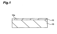
- a GaN substrate 10 is prepared.
- the GaN substrate 10 may be made of GaN single crystal.
- the GaN substrate 10 is placed in the MOCVD apparatus (not shown) and the temperature of the GaN substrate 10 is increased to a temperature of 1050 degrees Celsius to carry out the thermal cleaning of the surface 10a of the GaN substrate 10.
- the thermal cleaning removes contaminants on the surface 10a and improves the evenness of the surface 10a.
- a gas including trimethylgallium (TMG) of a III group element source, ammonia (NH 3 ) of a V group element source and silane (SiH 4 ) of a doping element source are supplied to the MOCVD apparatus to form an n-type GaN buffer layer 12 on the surface 10a of the GaN substrate 10.
- TMG trimethylgallium
- NH 3 ammonia
- SiH 4 silane
- the epitaxial growth temperature is 1050 degrees Celsius.
- the thickness of the GaN buffer layer 12 is 0.5 micrometers.
- the temperature of the GaN substrate 10 is decreased to 800 degrees Celsius, and a gas including TMG and trimethylindium (TMI) of III group element sources and NH 3 of a V group element source are supplied to the MOCVD apparatus to form an In X Ga 1-X N layer 14 on the GaN buffer 12, as shown in Fig. 2.
- a gas including TMG and trimethylindium (TMI) of III group element sources and NH 3 of a V group element source are supplied to the MOCVD apparatus to form an In X Ga 1-X N layer 14 on the GaN buffer 12, as shown in Fig. 2.
- TMG and trimethylindium (TMI) of III group element sources and NH 3 of a V group element source are supplied to the MOCVD apparatus to form an In X Ga 1-X N layer 14 on the GaN buffer 12, as shown in Fig. 2.
- TMG and trimethylindium (TMI) of III group element sources and NH 3 of a V group element source are supplied to the MOCVD apparatus to form an In X Ga 1-X
- GaN-based layers The formation of GaN-based layers will be described with reference to Fig. 3.
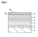
- the temperature of the substrate 10 is increased to 1100 degrees Celsius, and a gas including TMG and TMA of III group element sources, NH 3 of a V group element source and SiH 4 of a doping element source are supplied to the MOCVD apparatus to form an n-type Al Y Ga 1-Y N (0 ⁇ Y ⁇ 1) layer 16 on the InGaN layer 14, as shown in Fig. 3.
- the composition Y of the n-type Al Y Ga 1-Y N layer 16 is 0.5 and the thickness of the Al Y Ga 1-Y N layer 16 is 0.2 micrometers.
- the formation of the remaining GaN-based layers will be described with reference to Fig. 3.
- a gas including TMG and TMA of III group element sources and NH 3 of a V group element source are supplied to the MOCVD apparatus to form an Al Z Ga 1-Z N light generating layer 18 (0 ⁇ Z ⁇ 1) on the AlGaN layer 16 without changing the substrate temperature.
- This gas may contain SiH 4 of a doping element source.
- the composition Z of the Al Z Ga 1-Z N light generating layer 18 is 0.05 and the thickness of the Al Z Ga 1-Z N layer 18 is 0.1 micrometers.
- a laser beam LB1 having the wavelength of 400 nanometers is irradiated to the backside of the GaN substrate 10.
- the irradiated light passes through the GaN substrate 10 and is absorbed by the InGaN layer 14.
- the irradiation of the laser light modifies the InGaN layer 14 and the modified InGaN layer weakens bonding force between the InGaN layer 14 and the GaN buffer layer 12 to separate one of the GaN substrate 10 and the InGaN layer 14 from the other.
- the surface exposed by this separation is polished to create the surface 16a of the n-type AlGaN layer 16.
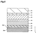
- the GaN substrate 10 used to deposit the AlGaN layers 16, 18 and 20 is lifted off from the AlGaN layers 16, 18 and 20.
- Cu-W alloy has a small thermal resistance and thus the Cu-W alloy substrate 26 prevents the optical output of the light emitting diode 1 from saturating in a high current injection.
- the p-electrode 22 is made of material that has a reflectivity higher than the Cu-W substrate 26, such as Ag, the light emitting diode 1 exhibits an excellent efficiency of light output.
- a semiconductor layer for lifting-off is made of material having a bandgap smaller than material of the substrate, such as InGaN semiconductor.
- the InGaN layer is formed on a substrate made of GaN-based material, such as a GaN substrate.
- the InGaN layer 14 receives a laser beam of the peak wavelength smaller than a wavelength corresponding to the bandgap energy of InGaN and greater than a wavelength corresponding to the bandgap energy of GaN semiconductor, such as a laser beam of wavelength, 400 nanometers.
- the irradiation of the laser beam permits the separation of one of the GaN substrate 10 and the AlGaN layers 16, 18 and 20 from the other by a lift-off method.
- the semiconductor light generating device such as the light emitting diode 1, includes a GaN-based semiconductor portion, an electrode and a conductive substrate.
- the GaN-based semiconductor portion includes a light generating layer.
- the light generating layer has a density of threading dislocations smaller than 1 ⁇ 10 7 per square centimeters (cm -2 ).
- the electrode is provided on the GaN-based semiconductor portion.
- the primary surface of the conductive substrate is bonded to the surface of the electrode by a conductive adhesive.
- the dimension of the primary surface of the conductive substrate is substantially equal to the dimension of the surface of the electrode.
- the thickness of the GaN-based semiconductor portion is smaller than that of the conductive substrate, and may be 10 micrometers at a maximum.
- the light emitting diode 1 can generate light of a peak wavelength, e.g., 350 nanometers, in an ultraviolet range and this wavelength is shorter than that of another light emitting diode having an InGaN light generation layer.
- Semiconductor light generating devices having one or more layers of AlGaN or nitride-based compound semiconductor containing aluminum are sensitive to threading dislocations as compared to a semiconductor light generating devices having one or more layers of InGaN, and the threading dislocations in the former device deteriorates the light generating efficiency as compared to the latter device.
- Diligent studies conducted by the inventors have found a solution: a method of manufacturing a light emitting diode using a GaN substrate, as described above.
- This light emitting diode has a light generating efficiency improved by lowering the density of threading dislocations using a substrate of GaN semiconductor having a lattice constant close to that of AlGaN as compared to sapphire.
- the density of threading dislocations of the AlGaN light generating layer 18 is equal to or less than 5 ⁇ 10 6 per square centimeters (cm -2 ) in the light emitting diode 1 fabricated by the above method, and this value is less than 1.0 ⁇ 10 7 per square centimeters (cm -2 ).
- a light emitting diode In GaN-based light emitting diodes, particularly to GaN-based ultraviolet light emitting diodes, threading dislocations in the light generating layers work as nonluminous recombination centers, and thus a light emitting diode that includes a light generating layer with a low density of threading dislocations has an excellent efficiency of light generation.
- a light emitting diode generates ultraviolet light of a power of 100 milliwatts and the peak wavelength of 350 nanometers at the current of 500 milliamperes.
- the light emitting diode 1 is fabricated by both the removal of the GaN substrate using the laser lift-off method and the bonding of the conductive substrate, and thus provides the light from the AlGaN light generating layer 18 in a high efficiency of light output without any absorption of the light by the GaN substrate.
- a substrate 10A of single crystal Al V Ga 1-V N (0 ⁇ V ⁇ 1) is prepared.
- the composition V of the substrate 10A is 0.18.
- the Al V Ga 1-V N substrate 10A is placed in an MOCVD apparatus to perform the thermal cleaning process of the Al V Ga 1-V N substrate 10A as is the GaN substrate in the first embodiment.
- the temperature of the thermal cleaning process is 1050 degrees Celsius.
- the temperature of the substrate 10A is decreased to 800 degrees Celsius, and a gas including TMG and TMI of III group element sources and NH 3 of a V group element source are supplied to the MOCVD apparatus to form a In X Ga 1-X N layer 14 on the Al W Ga 1-W N buffer layer 12A, as shown in Fig. 8.
- a gas including TMG and TMI of III group element sources and NH 3 of a V group element source are supplied to the MOCVD apparatus to form a In X Ga 1-X N layer 14 on the Al W Ga 1-W N buffer layer 12A, as shown in Fig. 8.
- the composition X of the In X Ga 1-X N layer 14 is 0.1 and the thickness of the In X Ga 1-X N layer 14 is 0.1 micrometers.
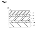
- the temperature of the substrate 10A is increased to 1100 degrees Celsius, and a gas including TMG and TMA of III group element sources, NH 3 of a V group element source and SiH 4 of a doping element source are supplied to the MOCVD apparatus to form an n-type Al Y Ga 1-Y N layer 16 on the InGaN layer 14, as shown in Fig. 9.
- a gas including TMG and TMA of III group element sources, NH 3 of a V group element source and SiH 4 of a doping element source are supplied to the MOCVD apparatus to form an n-type Al Y Ga 1-Y N layer 16 on the InGaN layer 14, as shown in Fig. 9.
- the composition Y of the n-type Al Y Ga 1-Y N layer 16 is 0.1 and the thickness of Al Y Ga 1-Y N layer 16 is 0.2 micrometers.
- a gas including TMG and TMA of III group element sources, NH 3 of a V group element source and Cp 2 Mg of a doping element source are supplied to the MOCVD apparatus to form a p-type Al U Ga 1-U N layer 20 on the light generating AlGaN layer 18, as shown in Fig. 9.
- the composition U of the Al U Ga 1-U N layer 20 is 0.1 and the thickness of the Al U Ga 1-U N layer 20 is 0.2 micrometers.
- a GaN-based semiconductor structure such as an AlGaN semiconductor structure including the AlGaN layers 16, 18 and 20, is provided on the AlGaN substrate 10A, as shown in Fig. 9.
- the AlGaN buffer layer 12A and the InGaN layer 14 are located between the GaN-based semiconductor structure and the AlGaN substrate 10A.
- the AlGaN substrate 10A and the epitaxial layers 12A, 14, 16, 18 and 20 formed thereon (thereinafter referred to as the epitaxial substrate) is taken out from the MOCVD apparatus, and the epitaxial substrate is placed in the metal deposition apparatus and a p-electrode film 22 of Ag is deposited on the surface 20a of the p-type AlGaN layer 20, as shown in Fig. 10.
- the p-electrode film 22 is heated at the temperature of 400 degrees Celsius for five minutes.
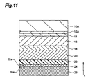
- the p-electrode film 22 is bonded to a metal substrate, such as a Cu-W alloy substrate 26, by use of a conductive adhesive, such as a Au-Sn solder layer 24, as shown in Fig. 11.
- a conductive adhesive such as a Au-Sn solder layer 24, as shown in Fig. 11.
- the melt point of Au-Sn solder is 280 degrees Celsius.
- the surface 22a of the p-electrode film 22 is bonded to the surface 26a of the Cu-W alloy substrate 26.
- the semiconductor substrate and layers 10A, 12A, 14, 16, 18 and 20 and the Cu-W alloy substrate 26 are integrated with each other to form a single member.
- laser beam LB2 having a wavelength of 400 nanometers is irradiated to the backside of the AlGaN substrate 10A.
- the irradiated light passes through the AlGaN substrate 10A and is absorbed by the InGaN layer 14.
- This absorption of the laser beam modifies the InGaN layer 14 and the modified InGaN layer weakens bonding force between the InGaN layer 14 and the buffer layer 12A to separate one of the AlGaN substrate 10A and the InGaN layer 14 from the other.
- the surface exposed by this separation is polished to create the surface 16a of the n-type AlGaN layer 16.
- the AlGaN substrate 10A used to deposit the AlGaN layers 16, 18 and 20 is lifted off from the AlGaN layers 16, 18 and 20.
- the Cu-W alloy has a small thermal resistance and thus the Cu-W alloy substrate 26 prevents the optical power of the light emitting diode 1 from saturating in a high injection of current.
- the p-electrode 22 is made of material that has a reflectivity higher than the Cu-W substrate 26, such as Ag, and thus the light emitting diode 1A exhibits an excellent efficiency of light output.
- the lifted-off AlGaN substrate 10A is polished to restore or recondition the surface thereof for reusing the AlGaN substrate 10A to make light emitting diodes.
- the reuse of the AlGaN substrate 10A reduces the manufacturing cost of the light emitting diode 1A.
- the semiconductor light generating device such as the light emitting diode 1A, includes a GaN-based semiconductor portion, an electrode and a conductive substrate.
- the GaN-based semiconductor portion includes a light generating layer.
- the light generating layer has a density of threading dislocations smaller than 1 ⁇ 10 7 square centimeters (cm -2 ).
- the electrode is provided on the GaN-based semiconductor portion.
- the primary surface of the conductive substrate is bonded to the surface of the electrode by a conductive adhesive.
- the dimension of the primary surface of the conductive substrate is substantially equal to the dimension of the surface of the electrode.
- the thickness of the GaN-based semiconductor portion is smaller than that of the conductive substrate, and may be 10 micrometers at a maximum.
- the light emitting diode 1A includes the light generating layer 18 as in light emitting diode 1.
- the light emitting diode 1A can generate light, for example, 350 nanometers, in an ultraviolet wavelength range (for example, 205 to 365 nanometers). The wavelength of this light is shorter than a wavelength of light generated by a light emitting diode having an InGaN light generating layer.
- the light emitting diode 1A is sensitive to threading dislocations as compared to a semiconductor light generating devices having one or more layers of InGaN. Diligent studies conducted by the inventors have found a solution of a method of manufacturing a light emitting diode using an AlGaN substrate as described above.
- the density of threading dislocations of the AlGaN light generating layer 18 is about 1.0 ⁇ 10 6 per square centimeters (cm -2 ) which is less than 1.0 ⁇ 10 7 per square centimeters (cm -2 ).
- GaN-based light emitting diodes particularly to ultraviolet light emitting diodes, threading dislocations in the light generating layers work as nonluminous recombination centers, and thus GaN-based light emitting diodes including a light generating layer with a low density of threading dislocations has an excellent efficiency of light generation.
- Such a light emitting diode generates ultraviolet light of 100 milliwatt power and the wavelength of 350 nanometers at the current of 500 milliamperes.
- the light emitting diode is fabricated by both the removal of the AlGaN substrate using a laser lift-off method and the bonding of the conductive substrate, and thus emits light from the AlGaN light generating layer 18 in a high output efficiency without the absorption of the light by the GaN substrate.
- the layers 16, 18 and 20 are formed on the AlGaN substrate 10A of a lattice constant approximately equal or close to that of AlGaN ,and thus the densities of threading dislocations in the AlGaN layers 16, 18 and 20 are reduced as compared to AlGaN layers grown on the sapphire substrate. Accordingly, the light emitting diode 1A has a high efficiency of light generation.
- the Au-Sn solder layer 24 which bonds the p-electrode 22 and the Cu-W alloy substrate 26 to each other has a small thermal resistance, and thus the light emitting diode 1A has a high efficiency of light generation even in the high injection of current.
- GaN-based semiconductor layers are not limited to the AlGaN layers, but GaN-based mixed semiconductor crystal containing indium, aluminum and so on, for example AlInGaN.
- the material of the conductive substrate is not limited to Cu-W alloy, and metal having a low thermal resistance, such as Fe-Ni alloy, can be also used for the conductive substrate.
- the conductive adhesive is not limited to Au-Sn solder, but Pb-Sn solder can also be used as the conductive adhesive.
- the composition of the AlGaN substrate and InGaN layers can be changed if required.
- the light generating device is limited to the light emitting diode and may be a laser diode.
- the separation of the GaN or AlGaN substrate from the GaN-based semiconductor layers is not limited to the laser lift-off method, and, for example, wet etching methods can be also used.
- the material of the p-electrode is not limited to silver (Ag), and conductive material which has a reflectively greater than that of the conductive substrate in the wavelength range of light from the light generating layer, aluminum (Al), rhodium (Rh) and so on can be also used.
Landscapes
- Led Devices (AREA)
Abstract
Description
In one example of the present invention, the conductive substrate is made of metal.
In this method, the light generating semiconductor device efficiently outputs light from the light generation layer.
In this method, although the GaN substrate is used, the GaN substrate is separated from the GaN-based semiconductor layers by irradiating the sacrifice layer with light having a component of a wavelength longer than that corresponding to the bandgap energy of GaN semiconductor, i.e., a laser lift-off method.
In this method, the separated GaN substrate can be used repeatedly to manufacture light generation semiconductor devices, thereby reducing costs for manufacturing the light generation semiconductor device.
In the method according to the present invention, the conductive substrate is made of metal.
In this method, the light generating semiconductor device efficiently outputs light from the light generation layer.
In this method, although the GaN substrate is used, the AlGaN substrate is separated from the GaN-based semiconductor layers by irradiating the sacrifice layer with light having a component of a wavelength longer than that corresponding to the bandgap energy of AlGaN semiconductor, i.e., a laser lift-off method.
In this method, the bandgap of the sacrifice layer is smaller than that of AlGaN semiconductor.
Having described and illustrated the principle of the invention in a preferred embodiment thereof, it is appreciated by those having skill in the art that the invention can be modified in arrangement and detail without departing from such principles. We therefore claim all modifications and variations coming within the spirit and scope of the following claims.
Claims (20)
- A method of making a semiconductor light generating device, the method comprising the steps of:forming a GaN-based semiconductor portion on a AlXGa1-XN (0 ≤ x ≤ 1) substrate, the GaN-based semiconductor portion including a light generating film;forming an electrode film on the GaN-based semiconductor portion;bonding a conductive substrate to a surface of the electrode film using a conductive adhesive; andafter bonding the conductive substrate, separating one of the AlXGa1-XN substrate and the GaN-based semiconductor portion from the other.
- The method according to claim 1, wherein the conductive substrate is made of metal.
- The method according to claim 1 or 2, wherein the AlXGa1-XN substrate is a GaN substrate.
- The method according to claim 3, the method further comprising the step of:wherein separating one of the GaN substrate and the GaN-based semiconductor film from the other includes a step of irradiating the sacrificial film with light to perform lift-off of one of the GaN substrate and the GaN-based semiconductor portion from the other, the light including a wavelength component corresponding to a energy smaller than a bandgap energy of GaN semiconductor.prior to forming the GaN-based semiconductor portion, forming a sacrificial film on the GaN substrate, the sacrificial film being made of a first material, the first material having a band gap smaller than the material of the substrate,
- The method according to claim 4, wherein the sacrificial film is made of nitride compound semiconductor containing indium.
- The method according to any one of claims 3 to 5, the method further comprising the steps of:reconditioning the separated GaN substrate for reuse; andperforming the following steps using the reconditioned GaN substrate:forming a GaN-based semiconductor portion on the reconditioned GaN substrate, the GaN-based semiconductor portion including a light generating film;forming an electrode film on the GaN-based semiconductor portion;bonding a conductive substrate to a surface of the electrode film; andafter bonding the conductive substrate, separating one of the reconditioned GaN substrate and the GaN-based semiconductor portion from the other.
- The method according to claim 1 or 2,
wherein the AlXGa1-XN substrate (0 ≤ x ≤ 1) is an AlXGa1-XN substrate (0 < x ≤ 1). - The method according to claim 7, the method comprising the step of:wherein separating one of the AlXGa1-XN substrate and the GaN-based semiconductor portion from the other includes a step of irradiating the sacrificial film with light to perform lift-off of one of the AlXGa1-XN substrate and the GaN-based semiconductor portion from the other, the light including a wavelength component corresponding to a energy smaller than a bandgap energy of material of the substrate.prior to forming the GaN-based semiconductor portion, forming a sacrificial film on the AlXGa1-XN substrate, the sacrificial layer being made of a first material, the first material having a bandgap smaller than material of the AlXGa1-XN substrate,
- The method according to claim 8, wherein the sacrificial layer is made of nitride compound semiconductor containing indium.
- The method according to any one of claims 7 to 9, the method further comprising the steps of:reconditioning the separated AlXGa1-XN substrate for reuse; andperforming the following steps using the reconditioned AlXGa1-XN substrate:forming a GaN-based semiconductor portion on the reconditioned AlXGa1-XN substrate, the GaN-based semiconductor portion including a light generating film;forming an electrode film on the GaN-based semiconductor portion;bonding a conductive substrate to a surface of the electrode film; andafter bonding the conductive substrate, separating one of the reconditioned AlXGa1-XN substrate and the GaN-based semiconductor portion from the other.
- The method according to any one of claims 1 to 10, wherein the light generating layer is made of material having a bandgap energy greater than material of the substrate.
- The method according to any one of claims 1 to 11, wherein the light generating film is made of nitride compound semiconductor containing aluminum.
- The method according to any one of claims 1 to 12, wherein the conductive substrate is made of one of Cu-W alloy and Fe-Ni alloy.
- The method according to any one of claims 1 to 13, wherein the conductive adhesive contains one of Au-Sn solder and Pb-Ni solder.
- The method according to any one of claims 1 to 14, wherein the electrode film is made of material having a reflectivity greater than the conductive substrate at a peak wavelength of light from the light generating layer.
- A semiconductor light generating device comprising:a GaN-based semiconductor portion including a light generating layer, the light generating layer having a density of threading dislocations smaller than 1 × 107 cm-2;an electrode provided on the GaN-based semiconductor portion;a conductive substrate bonded to a surface of the electrode by a conductive adhesive.
- The semiconductor light generating device according to claim 16, wherein the light generating layer is made of a GaN-based semiconductor having a bandgap energy greater than GaN semiconductor.
- The semiconductor light generating device according to claim 16, wherein the light generating layer is made of a semiconductor material of a bandgap energy greater than AlXGa1-XN (0 < x ≤ 1).
- The semiconductor light generating device according to any one of claims 16 to 18, wherein the electrode is made of material having a reflectivity greater than the conductive substrate at a peak wavelength of light from the light generating layer.
- The semiconductor light generating device according to any one of claims 16 to 19, wherein the light generating layer is made of a nitride-based compound semiconductor containing aluminum.
Applications Claiming Priority (4)
| Application Number | Priority Date | Filing Date | Title |
|---|---|---|---|
| JP2003290308 | 2003-08-08 | ||
| JP2003290308 | 2003-08-08 | ||
| JP2004171301A JP4218597B2 (en) | 2003-08-08 | 2004-06-09 | Manufacturing method of semiconductor light emitting device |
| JP2004171301 | 2004-06-09 |
Publications (2)
| Publication Number | Publication Date |
|---|---|
| EP1505661A2 true EP1505661A2 (en) | 2005-02-09 |
| EP1505661A3 EP1505661A3 (en) | 2009-01-07 |
Family
ID=33554539
Family Applications (1)
| Application Number | Title | Priority Date | Filing Date |
|---|---|---|---|
| EP04018710A Withdrawn EP1505661A3 (en) | 2003-08-08 | 2004-08-06 | GaN-based LED and its manufacturing method |
Country Status (6)
| Country | Link |
|---|---|
| US (2) | US7368310B2 (en) |
| EP (1) | EP1505661A3 (en) |
| JP (1) | JP4218597B2 (en) |
| KR (1) | KR101161917B1 (en) |
| CN (1) | CN100461468C (en) |
| TW (1) | TW200507307A (en) |
Cited By (5)
| Publication number | Priority date | Publication date | Assignee | Title |
|---|---|---|---|---|
| EP1768194A3 (en) * | 2005-09-22 | 2009-12-09 | Sanyo Electric Co., Ltd. | Method of manufacturing nitride semiconductor device |
| EP2365535A3 (en) * | 2010-03-09 | 2012-10-10 | LG Innotek Co., Ltd. | Substrate for fabricating light emitting device and method for fabricating the light emitting device |
| EP1727218A3 (en) * | 2005-05-27 | 2014-01-22 | LG Electronics, Inc. | Method of manufacturing light emitting diodes |
| EP2475016A3 (en) * | 2011-01-05 | 2014-10-08 | Samsung Electronics Co., Ltd. | Method of manufacturing light emitting diode and light emitting diode manufactured thereby |
| EP2363895A3 (en) * | 2010-03-05 | 2016-02-17 | LG Innotek Co., Ltd. | Light emitting device, method of manufacturing the same, light emitting device package |
Families Citing this family (46)
| Publication number | Priority date | Publication date | Assignee | Title |
|---|---|---|---|---|
| US8318519B2 (en) * | 2005-01-11 | 2012-11-27 | SemiLEDs Optoelectronics Co., Ltd. | Method for handling a semiconductor wafer assembly |
| US8802465B2 (en) | 2005-01-11 | 2014-08-12 | SemiLEDs Optoelectronics Co., Ltd. | Method for handling a semiconductor wafer assembly |
| JP2006202845A (en) * | 2005-01-18 | 2006-08-03 | Sony Corp | Semiconductor light emitting device |
| US20060267043A1 (en) * | 2005-05-27 | 2006-11-30 | Emerson David T | Deep ultraviolet light emitting devices and methods of fabricating deep ultraviolet light emitting devices |
| KR100706952B1 (en) * | 2005-07-22 | 2007-04-12 | 삼성전기주식회사 | Vertical structure gallium nitride-based light emitting diode device and method of manufacturing the same |
| JPWO2007023911A1 (en) * | 2005-08-25 | 2009-03-26 | 株式会社 東北テクノアーチ | Semiconductor substrate manufacturing method |
| WO2007049939A1 (en) * | 2005-10-29 | 2007-05-03 | Samsung Electronics Co., Ltd. | Semiconductor device and method of fabricating the same |
| JP2007134388A (en) * | 2005-11-08 | 2007-05-31 | Sharp Corp | Nitride-based semiconductor device and manufacturing method thereof |
| JP2007221051A (en) * | 2006-02-20 | 2007-08-30 | Sanyo Electric Co Ltd | Nitride semiconductor device manufacturing method |
| WO2007097242A1 (en) * | 2006-02-24 | 2007-08-30 | Matsushita Electric Industrial Co., Ltd. | Light-emitting device |
| US7696523B2 (en) * | 2006-03-14 | 2010-04-13 | Lg Electronics Inc. | Light emitting device having vertical structure and method for manufacturing the same |
| US8373195B2 (en) | 2006-04-12 | 2013-02-12 | SemiLEDs Optoelectronics Co., Ltd. | Light-emitting diode lamp with low thermal resistance |
| US7863639B2 (en) * | 2006-04-12 | 2011-01-04 | Semileds Optoelectronics Co. Ltd. | Light-emitting diode lamp with low thermal resistance |
| JP4714087B2 (en) | 2006-06-14 | 2011-06-29 | 住友電気工業株式会社 | GaN substrate storage method and semiconductor device manufacturing method |
| US8476158B2 (en) | 2006-06-14 | 2013-07-02 | Sumitomo Electric Industries, Ltd. | Method of preparing and storing GaN substrate, prepared and stored GaN substrate, and semiconductor device and method of its manufacture |
| KR100818451B1 (en) | 2006-07-03 | 2008-04-01 | 삼성전기주식회사 | Semiconductor light emitting device having polarization |
| JP2008294213A (en) * | 2007-05-24 | 2008-12-04 | Sanyo Electric Co Ltd | Semiconductor device and manufacturing method thereof |
| JP2008294379A (en) * | 2007-05-28 | 2008-12-04 | Sanyo Electric Co Ltd | Manufacturing method of nitride-based semiconductor element |
| US20080303033A1 (en) * | 2007-06-05 | 2008-12-11 | Cree, Inc. | Formation of nitride-based optoelectronic and electronic device structures on lattice-matched substrates |
| CN101330117B (en) * | 2007-06-18 | 2012-04-18 | 周明奇 | Method for preparing illuminating device using zinc oxide |
| JP4937025B2 (en) * | 2007-07-20 | 2012-05-23 | 三洋電機株式会社 | Semiconductor laser device and manufacturing method thereof |
| JP2009141093A (en) * | 2007-12-06 | 2009-06-25 | Toshiba Corp | Light emitting device and method for manufacturing light emitting device |
| DE102009018603B9 (en) | 2008-04-25 | 2021-01-14 | Samsung Electronics Co., Ltd. | Lighting device and manufacturing method thereof |
| FR2936903B1 (en) * | 2008-10-07 | 2011-01-14 | Soitec Silicon On Insulator | RELAXING A LAYER OF CONTAMINATED MATERIAL WITH APPLICATION OF A STIFFENER |
| KR101408475B1 (en) | 2008-10-30 | 2014-06-19 | 소이텍 | Methods of forming layers of semiconductor material having reduced lattice strain, semiconductor structures, devices and engineered substrates including same |
| US8637383B2 (en) | 2010-12-23 | 2014-01-28 | Soitec | Strain relaxation using metal materials and related structures |
| JP5712471B2 (en) * | 2009-08-03 | 2015-05-07 | 富士通株式会社 | Method for manufacturing compound semiconductor device |
| EP2330697A1 (en) * | 2009-12-07 | 2011-06-08 | S.O.I.Tec Silicon on Insulator Technologies | Semiconductor device having an InGaN layer |
| WO2011069242A1 (en) * | 2009-12-09 | 2011-06-16 | Cooledge Lighting Inc. | Semiconductor dice transfer-enabling apparatus and method for manufacturing transfer-enabling apparatus |
| KR101460086B1 (en) | 2009-12-15 | 2014-11-10 | 소이텍 | Process for recycling a substrate |
| US20110151588A1 (en) * | 2009-12-17 | 2011-06-23 | Cooledge Lighting, Inc. | Method and magnetic transfer stamp for transferring semiconductor dice using magnetic transfer printing techniques |
| US8334152B2 (en) * | 2009-12-18 | 2012-12-18 | Cooledge Lighting, Inc. | Method of manufacturing transferable elements incorporating radiation enabled lift off for allowing transfer from host substrate |
| KR101160158B1 (en) * | 2010-05-28 | 2012-06-27 | 주식회사 엘티에스 | substrate detaching apparatus of LLO process |
| TW201225361A (en) * | 2010-11-09 | 2012-06-16 | Semileds Optoelectronics Co | Light-emitting diode lamp with low thermal resistance |
| KR101717670B1 (en) * | 2011-06-15 | 2017-03-17 | 삼성전자주식회사 | Method for manufacturing light emitting diode |
| KR20140014625A (en) * | 2012-07-25 | 2014-02-06 | 서울바이오시스 주식회사 | Method of fabricating gallium nitrded based semiconductor device |
| KR101923673B1 (en) * | 2012-09-13 | 2018-11-29 | 서울바이오시스 주식회사 | Method of fabricating gallium nitrded based semiconductor device |
| JP2014175427A (en) * | 2013-03-07 | 2014-09-22 | Toshiba Corp | Semiconductor light-emitting element and method of manufacturing the same |
| JP2013128150A (en) * | 2013-03-26 | 2013-06-27 | Toyoda Gosei Co Ltd | Method of manufacturing group-iii nitride semiconductor light-emitting element |
| FR3009644B1 (en) * | 2013-08-08 | 2016-12-23 | Soitec Silicon On Insulator | METHOD, STACK AND ASSEMBLY FOR SEPARATING A STRUCTURE OF A SUBSTRATE BY ELECTROMAGNETIC IRRADIATION |
| KR102288238B1 (en) * | 2013-09-03 | 2021-08-09 | 가부시키가이샤 한도오따이 에네루기 켄큐쇼 | Light-emitting device |
| JP2015153826A (en) * | 2014-02-12 | 2015-08-24 | ウシオ電機株式会社 | Nitride semiconductor light emitting element and manufacturing method of the same |
| KR20210123064A (en) * | 2020-04-02 | 2021-10-13 | 웨이브로드 주식회사 | Method of manufacturing a iii-nitride semiconducter device |
| JP7553915B2 (en) * | 2020-04-15 | 2024-09-19 | 国立大学法人東海国立大学機構 | Method for manufacturing a gallium nitride semiconductor device |
| JP7639390B2 (en) * | 2021-02-23 | 2025-03-05 | 株式会社デンソー | Semiconductor chip manufacturing method |
| KR102615809B1 (en) * | 2022-07-22 | 2023-12-20 | 웨이브로드 주식회사 | Gruop 3 nitride semiconductor template for power semiconductor device |
Citations (4)
| Publication number | Priority date | Publication date | Assignee | Title |
|---|---|---|---|---|
| WO2002019439A1 (en) | 2000-08-31 | 2002-03-07 | Osram Opto Semiconductors Gmbh | Method for producing a radiation-emitting semiconductor chip based on iii-v nitride semiconductor material, and a corresponding radiation-emitting semiconductor chip |
| US20020166502A1 (en) | 1994-01-27 | 2002-11-14 | Vaudo Robert P. | Low defect density (Ga, Al, In) N and HVPE process for making same |
| US6552376B1 (en) | 1999-09-01 | 2003-04-22 | Toyoda Gosei Co., Ltd. | Group III nitride compound semiconductor device |
| US20030089906A1 (en) | 2001-11-13 | 2003-05-15 | Matsushita Electric Industrial Co., Ltd. | Semiconductor device and method for fabricating the same |
Family Cites Families (16)
| Publication number | Priority date | Publication date | Assignee | Title |
|---|---|---|---|---|
| CN1044840C (en) * | 1997-07-24 | 1999-08-25 | 北京大学 | Method of using GaN/Al2O3 composite material as substrate in the epitaxial growth of III-V family nitride |
| JP3914615B2 (en) | 1997-08-19 | 2007-05-16 | 住友電気工業株式会社 | Semiconductor light emitting device and manufacturing method thereof |
| JP3770014B2 (en) * | 1999-02-09 | 2006-04-26 | 日亜化学工業株式会社 | Nitride semiconductor device |
| JP3609661B2 (en) | 1999-08-19 | 2005-01-12 | 株式会社東芝 | Semiconductor light emitting device |
| JP2001148544A (en) | 1999-09-10 | 2001-05-29 | Sharp Corp | Semiconductor light emitting device |
| JP2001119104A (en) | 1999-10-21 | 2001-04-27 | Matsushita Electric Ind Co Ltd | Semiconductor manufacturing method |
| US6469320B2 (en) * | 2000-05-25 | 2002-10-22 | Rohm, Co., Ltd. | Semiconductor light emitting device |
| US6586819B2 (en) * | 2000-08-14 | 2003-07-01 | Nippon Telegraph And Telephone Corporation | Sapphire substrate, semiconductor device, electronic component, and crystal growing method |
| JP2002134822A (en) * | 2000-10-24 | 2002-05-10 | Sharp Corp | Semiconductor light emitting device and method of manufacturing the same |
| JP3639789B2 (en) * | 2001-01-31 | 2005-04-20 | シャープ株式会社 | Nitride semiconductor light emitting device |
| US6806508B2 (en) | 2001-04-20 | 2004-10-19 | General Electic Company | Homoepitaxial gallium nitride based photodetector and method of producing |
| JP3862602B2 (en) | 2001-05-18 | 2006-12-27 | 松下電器産業株式会社 | Manufacturing method of semiconductor device |
| JP2003100705A (en) | 2001-09-27 | 2003-04-04 | Toshiba Corp | Compound semiconductor element recovery device, element recovery method, element decomposition and purification method, compound semiconductor etching device, etching method, and compound semiconductor device manufacturing method |
| US6881261B2 (en) * | 2001-11-13 | 2005-04-19 | Matsushita Electric Industrial Co., Ltd. | Method for fabricating semiconductor device |
| WO2003054937A1 (en) | 2001-12-20 | 2003-07-03 | Matsushita Electric Industrial Co., Ltd. | Method for making nitride semiconductor substrate and method for making nitride semiconductor device |
| TWI278995B (en) * | 2002-01-28 | 2007-04-11 | Nichia Corp | Nitride semiconductor element with a supporting substrate and a method for producing a nitride semiconductor element |
-
2004
- 2004-06-09 JP JP2004171301A patent/JP4218597B2/en not_active Expired - Fee Related
- 2004-08-05 US US10/911,653 patent/US7368310B2/en not_active Expired - Fee Related
- 2004-08-06 KR KR1020040061869A patent/KR101161917B1/en not_active Expired - Fee Related
- 2004-08-06 EP EP04018710A patent/EP1505661A3/en not_active Withdrawn
- 2004-08-06 CN CNB2004100563402A patent/CN100461468C/en not_active Expired - Fee Related
- 2004-08-06 TW TW093123724A patent/TW200507307A/en not_active IP Right Cessation
-
2008
- 2008-02-21 US US12/071,440 patent/US7550776B2/en not_active Expired - Fee Related
Patent Citations (4)
| Publication number | Priority date | Publication date | Assignee | Title |
|---|---|---|---|---|
| US20020166502A1 (en) | 1994-01-27 | 2002-11-14 | Vaudo Robert P. | Low defect density (Ga, Al, In) N and HVPE process for making same |
| US6552376B1 (en) | 1999-09-01 | 2003-04-22 | Toyoda Gosei Co., Ltd. | Group III nitride compound semiconductor device |
| WO2002019439A1 (en) | 2000-08-31 | 2002-03-07 | Osram Opto Semiconductors Gmbh | Method for producing a radiation-emitting semiconductor chip based on iii-v nitride semiconductor material, and a corresponding radiation-emitting semiconductor chip |
| US20030089906A1 (en) | 2001-11-13 | 2003-05-15 | Matsushita Electric Industrial Co., Ltd. | Semiconductor device and method for fabricating the same |
Cited By (6)
| Publication number | Priority date | Publication date | Assignee | Title |
|---|---|---|---|---|
| EP1727218A3 (en) * | 2005-05-27 | 2014-01-22 | LG Electronics, Inc. | Method of manufacturing light emitting diodes |
| EP1768194A3 (en) * | 2005-09-22 | 2009-12-09 | Sanyo Electric Co., Ltd. | Method of manufacturing nitride semiconductor device |
| US7759219B2 (en) | 2005-09-22 | 2010-07-20 | Sanyo Electric Co., Ltd. | Method of manufacturing nitride semiconductor device |
| EP2363895A3 (en) * | 2010-03-05 | 2016-02-17 | LG Innotek Co., Ltd. | Light emitting device, method of manufacturing the same, light emitting device package |
| EP2365535A3 (en) * | 2010-03-09 | 2012-10-10 | LG Innotek Co., Ltd. | Substrate for fabricating light emitting device and method for fabricating the light emitting device |
| EP2475016A3 (en) * | 2011-01-05 | 2014-10-08 | Samsung Electronics Co., Ltd. | Method of manufacturing light emitting diode and light emitting diode manufactured thereby |
Also Published As
| Publication number | Publication date |
|---|---|
| US7368310B2 (en) | 2008-05-06 |
| EP1505661A3 (en) | 2009-01-07 |
| US20050040425A1 (en) | 2005-02-24 |
| JP4218597B2 (en) | 2009-02-04 |
| US20080149954A1 (en) | 2008-06-26 |
| JP2005093988A (en) | 2005-04-07 |
| TWI345315B (en) | 2011-07-11 |
| CN1581525A (en) | 2005-02-16 |
| TW200507307A (en) | 2005-02-16 |
| KR101161917B1 (en) | 2012-07-18 |
| KR20050016184A (en) | 2005-02-21 |
| US7550776B2 (en) | 2009-06-23 |
| CN100461468C (en) | 2009-02-11 |
Similar Documents
| Publication | Publication Date | Title |
|---|---|---|
| US7368310B2 (en) | Light generating semiconductor device and method of making the same | |
| Mukai et al. | Ultraviolet InGaN and GaN single-quantum-well-structure light-emitting diodes grown on epitaxially laterally overgrown GaN substrates | |
| US11251330B2 (en) | Pseudomorphic electronic and optoelectronic devices having planar contacts | |
| US8154009B1 (en) | Light emitting structure including high-al content MQWH | |
| CN101180741B (en) | AlInGaP LEDs with reduced temperature dependence | |
| KR101042417B1 (en) | Group III nitride semiconductor light emitting device and method of manufacturing the same, and lamp | |
| US20100270548A1 (en) | Semiconductor element and method of making same | |
| JP2010212738A (en) | Method of fabricating nitride-based resonator semiconductor structure | |
| JPWO2000016455A1 (en) | Semiconductor light emitting element and semiconductor laser | |
| US7910154B2 (en) | Nitride-based light emitting devices and methods of manufacturing the same | |
| US7554122B2 (en) | Nitride semiconductor light emitting device, and method of fabricating nitride semiconductor light emitting device | |
| US6191439B1 (en) | Semiconductor light emitting device | |
| US5963787A (en) | Method of producing gallium nitride semiconductor light emitting device | |
| US20230268462A1 (en) | Fully transparent ultraviolet or far-ultraviolet light-emitting diodes | |
| US6639258B2 (en) | Group III nitride compound semiconductor device | |
| JP2007221051A (en) | Nitride semiconductor device manufacturing method | |
| JP2005203419A (en) | Epitaxial wafer for light emitting device | |
| JP2004179369A (en) | Semiconductor device and manufacturing method thereof | |
| JP2005340762A (en) | Group iii nitride semiconductor light-emitting element | |
| JP2005311119A (en) | Gallium nitride-based light emitting device | |
| Mukai et al. | GaN-based light-emitting diodes suitable for white light | |
| JP2008277356A (en) | Semiconductor element | |
| Ohba | Near-UV LEDs on sapphire using single crystal AlN-buffer |
Legal Events
| Date | Code | Title | Description |
|---|---|---|---|
| PUAI | Public reference made under article 153(3) epc to a published international application that has entered the european phase |
Free format text: ORIGINAL CODE: 0009012 |
|
| AK | Designated contracting states |
Kind code of ref document: A2 Designated state(s): AT BE BG CH CY CZ DE DK EE ES FI FR GB GR HU IE IT LI LU MC NL PL PT RO SE SI SK TR |
|
| AX | Request for extension of the european patent |
Extension state: AL HR LT LV MK |
|
| PUAL | Search report despatched |
Free format text: ORIGINAL CODE: 0009013 |
|
| AK | Designated contracting states |
Kind code of ref document: A3 Designated state(s): AT BE BG CH CY CZ DE DK EE ES FI FR GB GR HU IE IT LI LU MC NL PL PT RO SE SI SK TR |
|
| AX | Request for extension of the european patent |
Extension state: AL HR LT LV MK |
|
| 17P | Request for examination filed |
Effective date: 20090513 |
|
| AKX | Designation fees paid |
Designated state(s): DE FR GB |
|
| 17Q | First examination report despatched |
Effective date: 20110329 |
|
| STAA | Information on the status of an ep patent application or granted ep patent |
Free format text: STATUS: THE APPLICATION IS DEEMED TO BE WITHDRAWN |
|
| 18D | Application deemed to be withdrawn |
Effective date: 20160301 |