EP1503496A1 - Photocurrent-to-voltage conversion apparatus including non-diode-connected clamping MOS transistor - Google Patents
Photocurrent-to-voltage conversion apparatus including non-diode-connected clamping MOS transistor Download PDFInfo
- Publication number
- EP1503496A1 EP1503496A1 EP04017901A EP04017901A EP1503496A1 EP 1503496 A1 EP1503496 A1 EP 1503496A1 EP 04017901 A EP04017901 A EP 04017901A EP 04017901 A EP04017901 A EP 04017901A EP 1503496 A1 EP1503496 A1 EP 1503496A1
- Authority
- EP
- European Patent Office
- Prior art keywords
- voltage
- mos transistor
- photocurrent
- conversion apparatus
- voltage conversion
- Prior art date
- Legal status (The legal status is an assumption and is not a legal conclusion. Google has not performed a legal analysis and makes no representation as to the accuracy of the status listed.)
- Granted
Links
Images






Classifications
-
- H—ELECTRICITY
- H03—ELECTRONIC CIRCUITRY
- H03F—AMPLIFIERS
- H03F3/00—Amplifiers with only discharge tubes or only semiconductor devices as amplifying elements
- H03F3/04—Amplifiers with only discharge tubes or only semiconductor devices as amplifying elements with semiconductor devices only
- H03F3/08—Amplifiers with only discharge tubes or only semiconductor devices as amplifying elements with semiconductor devices only controlled by light
- H03F3/082—Amplifiers with only discharge tubes or only semiconductor devices as amplifying elements with semiconductor devices only controlled by light with FET's
Definitions
- the present invention relates to a photocurrent-to-voltage conversion apparatus including a clamping MOS transistor.
- a photocoupler in order to electrically isolate an input from an output in a servo controller, a sequencer, an inverter or the like, a photocoupler has been developed.
- a photocurrent-to-voltage conversion apparatus is used in a light receiving circuit thereof.
- a photocurrent-to-voltage conversion apparatus is used in a light detection circuit in infrared communication or optical cable communication.
- a photocurrent-to-voltage conversion apparatus is used in a light detection circuit for converting a laser reflection signal into an electrical digital signal of an optical disc unit.
- a first prior art photocurrent-to-voltage conversion apparatus for a photodiode is constructed by an operational amplifier connected to the cathode of the photodiode and a negative feedback resistor connected between an output and an input of the operational amplifier (see: Fig. 4 of JP-A-61-41213). This will be explained later in detail.
- a diode serving as a clamp element is connected in parallel with the negative feedback resistor of the first prior art photocurrent-to-voltage conversion apparatus (see: Fig. 5 of JP-A-61-41213).
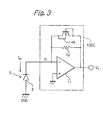
- a diode-connected N-channel MOS transistor serving as a clamp element is connected in parallel with the negative feedback resistor of the first prior art photocurrent-to-voltage conversion apparatus (see: Fig. 1 of JP-A-61-41213).
- the second and third photocurrent-to-voltage conversion apparatuses also will be explained later in detail.
- Another object is to provide a photocurrent-to-voltage conversion apparatus capable of obtaining an expected clamped level of the detection voltage, where the saturated voltage of the operational amplifier is large.
- an amplifier in a photocurrent-to-voltage conversion apparatus for converting a photocurrent flowing through a light receiving element into a detection voltage, an amplifier, a feedback resistor and a clamping MOS transistor are provided.
- the amplifier has an input connected to the light receiving element and an output for generating the detection voltage, and includes (2n + 1) inverter stages connected in series where n is 1, 2 ⁇ .
- the feedback resistor and the clamping transistor are connected between the output and input of the amplifier.
- the clamping MOS transistor is controlled by an output voltage of a non-final inverter one of the inverter stages.
- a photocurrent-to-voltage conversion apparatus 100A is connected to a cathode of a photodiode 2 whose anode is grounded.
- a reverse bias voltage is applied to the photodiode 2. Therefore, when the photodiode 2 receives a light signal S, a photocurrent I pd flows from the cathode to the anode.
- the photocurrent-to-voltage conversion apparatus 100A converts the photocurrent I pd into a detection voltage V d .
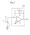
- the photocurrent-to-voltage conversion apparatus 100A is constructed by an operational amplifier 11 of a differential amplifier type having a grounded non-inverting input and an inverting input connected to the cathode of the photodiode 2, and a negative feedback resistor 12 connected between the output and inverting input of the operational amplifier 11.
- the operational amplifier 11 is constructed by a differential amplifier and a push-pull output circuit in response to the output signals of the differential amplifier.
- this photocurrent-to-voltage conversion apparatus 100B is constructed by a diode 13 serving as a clamp element connected in parallel with the negative feedback resistor 12 of Fig. 1, in order to suppress the waveform distortion between the light signal S and the detection signal V d . That is, when the strength of the light signal S is small, the diode 13 is not turned 0N, so that the detection voltage V d has a linear characteristic relative to the strength of the light signal S depending on the negative feedback resistor 12.
- this photocurrent-to-voltage conversion apparatus 100C is constructed by a diode-connected N-channel enhancement-type MOS transistor 14N serving as a clamp element connected in parallel with the negative feedback resistor 12 of Fig. 1, in order to suppress the waveform distortion between the light signal S and the detection signal V d . That is, when the strength of the light signal S is small, the transistor 14N is not turned ON, so that the detection voltage V d has a linear characteristic relative to the strength of the light signal S depending on the negative feedback resistor 12.
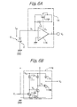
- this photocurrent-to-voltage conversion apparatus 1A is constructed by a P-channel enhancement-type MOS transistor 15P instead of the N-channel enhancement-type MOS transistor 14N of Fig. 3.
- a clamp voltage V CL of the P-channel enhancement-type MOS transistor 15P is determined by the absolute value of a threshold voltage V thp of the P-channel MOS transistor 15P.
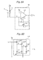
- the photocurrent-to-voltage conversion apparatus 1A is constructed by an operational amplifier 11N of an N-channel inverter type instead of the operational amplifier 11 of Fig. 3.
- the P-channel enhancement-type MOS transistor 15P is non-diode-connected, i.e., the gate of the P-channel MOS transistor 15P is connected to an intermediate stage of the operational amplifier 11N.
- the operational amplifier 11N is constructed by a plurality of inverter stages which are in this case three inverter stages.
- the first stage is formed by a constant current source 111 and an N-channel enhancement-type MOS transistor 112N connected in series between a power supply terminal V DD and a ground terminal GND
- the second stage is formed by a constant current source 113 and an N-channel enhancement-type MOS transistor 114N connected in series between the power supply terminal V DD and the ground terminal GND
- the final stage is formed by a constant current source 115 and an N-channel enhancement-type MOS transistor 116N connected in series between the power supply terminal V DD and the ground terminal GND.
- the constant current sources 111, 113 and 115 have the same driving power as each other, and the N-channel enhancement-type MOS transistors 112N, 114N and 116N have the same size as each other, so that the N-channel enhancement-type MOS transistors 112N, 114N and 116N have the same threshold voltage V thn0 .
- V 1 , V 2 and V 3 designates an input voltage of the first inverter stage (111, 112N), an output voltage of the first inverter stage (111, 112N) and an output voltage of the second inverter stage (113, 114N), respectively.
- the detection voltage V d is derived from the output of the final inverter stage (115, 116N), while the gate voltage of the MOS transistor 15P is derived from the output voltage V 3 of the second inverter stage (113, 114N).
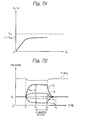
- the photocurrent-to-voltage conversion apparatus 1A of Fig. 6A is effective when the saturated voltage of the operational amplifier 11N is small so that the saturated difference between the detection voltage V d and the voltage V 1 is smaller than a clamp voltage V CL determined by a threshold voltage V thp of the P-channel MOS transistor 15P.
- V 0 is a reverse bias voltage determined by the threshold voltage V thn0 of the N-channel enhancement-type MOS transistors 112N, 114N and 116N.
- a photocurrent I pd flows therethrough.
- the photocurrent I pd flows through the negative feedback resistor 12, so that the voltage V 1 at the input of the first inverter (111, 112N) is decreased from V 0 .
- the decrease of the voltage V 1 is inversely-amplified by the first inverter stage (111, 112N) with respect to the voltage V 0 to increase the voltage V 2 .
- the increase of the voltage V 2 is inversely-amplified by the second inverter stage (113, 114N) with respect to the voltage V 0 to decrease the voltage V 3 .
- the decrease of the voltage V 3 is inversely-amplified by the third inverter stage (115, 116N) with respect to the voltage V 0 to increase the detection voltage V d .
- the P-channel MOS transistor 15P since the P-channel MOS transistor 15P enters a clamped state before the operational amplifier 11N is saturated, the saturation of the operational amplifier 11N can be suppressed.
- this photocurrent-to-voltage conversion apparatus 1B is connected to the anode of the photodiode 2 whose cathode is connected to the power supply terminal V DD .
- This photocurrent-to-voltage conversion apparatus 1B is constructed by an N-channel enhancement-type MOS transistor 15N instead of the P-channel enhancement-type MOS transistor 15P of Fig. 6A.
- a clamp voltage V CL of the N-channel enhancement-type MOS transistor 15N is determined by the absolute value of a threshold voltage V thn of the N-channel MOS transistor 15N.
- the photocurrent-to voltage conversion apparatus 1B is constructed by an operational amplifier 11P of a P-channel inverter type instead of the operational amplifier 11N of Fig. 6A.
- the N-channel enhancement-type MOS transistor 15N is non-diode-connected, i.e., the gate of the N-channel MOS transistor 15N is connected to an intermediate stage of the operational amplifier 11P.
- the operational amplifier 11P is constructed by a plurality of inverter stages which are in this case three inverter stages where P-channel enhancement-type MOS transistors 112P, 114P and 116P are provided instead of the N-channel enhancement-type MOS transistors 112N, 114N and 116N, respectively, of Fig 6B.
- the P-channel enhancement-type MOS transistors 112P, 114P and 116P have the same size as each other, so that the P-channel enhancement-type MOS transistors 112P, 114P and 116P have the same threshold voltage V thp0 .
- the photocurrent-to-voltage conversion apparatus 1B of Fig. 8A is effective when the saturated voltage of the operational amplifier 11B is small so that the saturated difference between the voltage V 1 and the detection voltage V d is smaller than a clamp voltage V CL determined by a threshold voltage V thn of the N-channel MOS transistor 15N.
- V 0 is a reverse bias voltage determined by the threshold voltage V thp0 of the P-channel enhancement-type MOS transistors 112P, 114P and 116P.
- a photocurrent I pd flows therethrough.
- the photocurrent I pd flows through the negative feedback resistor 12, so that the voltage V 1 at the input of the first inverter (111, 112P) is increased from V 0 .
- the increase of the voltage V 1 is inversely-amplified by the first inverter stage (111, 112P) with respect to the voltage V 0 to decrease the voltage V 2 .
- the decrease of the voltage V 2 is inversely-amplified by the second inverter stage (113, 114P) with respect to the voltage V 0 to increase the voltage V 3 .
- the N-channel MOS transistor 15N since the N-channel MOS transistor 15N enters a clamped state before the operational amplifier 11P is saturated, the saturation of the operational amplifier 11P can be suppressed.
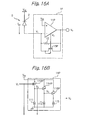
- Fig. 10A which illustrates a second embodiment of the photocurrent-to-voltage conversion apparatus according to the present invention
- the gate voltage of the MOS transistor 15P of this photocurrent-to-voltage conversion apparatus 1C is derived from the output voltage V 2 of the first inverter stage (111, 112N) as illustrated in Fig. 10B.
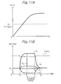
- the photocurrent-to-voltage conversion apparatus 1C of Fig. 10A is effective when the saturated voltage of the operational amplifier 11N is large so that the saturated difference between the detection voltage V d and the voltage V 1 is larger than the clamp voltage V CL determined by the threshold voltage V thp of the P-channel MOS transistor 15P.
- V 0 is a reverse bias voltage determined by the threshold voltage V thn0 of the N-channel enhancement-type MOS transistors 112N, 114N and 116N.
- a photocurrent I pd flows therethrough.
- the photocurrent I pd flows through the negative feedback resistor 12, so that the voltage V 1 at the input of the first inverter (111, 112N) is decreased from V 0 .
- the decrease of the voltage V 1 is inversely-amplified by the first inverter stage (111, 112N) with respect to the voltage V 0 to increase the voltage V 2 .
- the increase of the voltage V 2 is inversely-amplified by the second inverter stage (113, 114N) with respect to the voltage V 0 to decrease the voltage V 3 .
- the decrease of the voltage V 3 is inversely-amplified by the third inverter stage (115, 116N) with respect to the voltage V 0 to increase the detection voltage V d .
- V 3 ⁇ V 1 ⁇ V 0 ⁇ V 2 ⁇ V d
- the clamped detection voltage V d can be increased to an expected level.
- this photocurrent-to-voltage conversion apparatus 1D is connected to the anode of the photodiode 2 whose cathode is connected to the power supply terminal V DD .
- This photocurrent-to-voltage conversion apparatus 1D is constructed by an N-channel enhancement-type MOS transistor 15N instead of the P-channel enhancement-type MOS transistor 15P of Fig. 10A.
- a clamp voltage V CL of the N-channel enhancement-type MOS transistor 15N is determined by a threshold voltage V thn of the N-channel MOS transistor 15N.
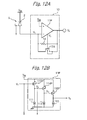
- the photocurrent-to-voltage conversion apparatus 1D is constructed by an operational amplifier 11P of a P-channel inverter type instead of the operational amplifier 11N of Fig. 10A.
- the N-channel enhancement-type MOS transistor 15N is non-diode-connected, i.e., the gate of the N-channel MOS transistor 15N is connected to an intermediate stage of the operational amplifier 11P, i.e., is derived from the output voltage V 2 of the first inverter stage (111, 112P) as illustrated in Fig. 12B.
- the operational amplifier 11P is constructed by a plurality of inverter stages which are in this case three inverter stages where P-channel enhancement-type MOS transistors 112P, 114P and 116P are provided instead of the N-channel enhancement-type MOS transistors 112N, 114N and 116N, respectively, of Fig. 10B.
- the P-channel enhancement-type MOS transistors 112P, 114P and 116P have the same size as each other, so that the P-channel enhancement-type MOS transistors 112P, 114P and 116P have the same threshold voltage V thp0 .
- the photocurrent-to-voltage conversion apparatus 1D of Fig. 12A is effective when the saturated voltage of the operational amplifier 11D is large so that the saturated difference between the voltage V 1 and the detection voltage V d is smaller than a clamp voltage V CL determined by a threshold voltage V thn of the N-channel MOS transistor 15N.
- V 0 is a reverse bias voltage determined by the threshold voltage V thp0 of the P-channel enhancement-type MOS transistors 112P, 114P and 116P.
- a photocurrent I pd flows therethrough.
- the photocurrent I pd flows through the negative feedback resistor 12, so that the voltage V 1 at the input of the first inverter (111, 112P) is increased from V 0 .
- the increase of the voltage V 1 is inversely-amplified by the first inverter stage (111, 112P) with respect to the voltage V 0 to decrease the voltage V 2 .
- the decrease of the voltage V 2 is inversely-amplified by the second inverter stage (113, 114P) with respect to the voltage V 0 to increase the voltage V 3 .
- the clamped detection voltage V d can be decreased to an expected level.
- photocurrent-to-voltage conversion apparatus 1E includes an N-channel enhancement-type MOS transistor 15N instead of the P-channel enhancement-type MOS transistor 15P of Fig. 10A.
- the gate voltage of the N-channel enhancement-type MOS transistor 15N is also derived from the output voltage V 2 of the first inverter stage (111, 112N) as illustrated in Fig. 14B.
- the photocurrent-to-voltage conversion apparatus 1E of Fig. 14A is effective when the saturated voltage of the operational amplifier 11N is large so that the saturated difference between the detection voltage V d and the voltage V 1 is larger than a clamp voltage V CL determined by the threshold voltage V thn of the N-channel MOS transistor 15N.
- V 0 is a reverse bias voltage determined by the threshold voltage V thn0 of the N-channel enhancement-type MOS transistors 112N, 114N and 116N.
- a photocurrent I pd flows therethrough.
- the photocurrent I pd flows through the negative feedback resistor 12, so that the voltage V, at the input of the first inverter (111, 112N) is decreased from V 0 .
- the decrease of the voltage V 1 is inversely-amplified by the first inverter stage (111, 112N) with respect to the voltage V 0 to increase the voltage V 2 .
- the increase of the voltage V 2 is inversely-amplified by the second inverter stage (113, 114N) with respect to the voltage V 0 to decrease the voltage V 3 .
- the decrease of the voltage V 3 is inversely-amplified by the third inverter stage (115, 116N) with respect to the voltage V 0 to increase the detection voltage V d .
- V 3 ⁇ V 1 ⁇ V 0 ⁇ V 2 ⁇ V d
- the clamped detection voltage V d can be increased to an expected level.
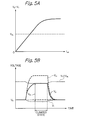
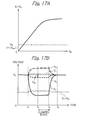
- the gate-to-source voltage of the N-channel MOS transistor 15N can be smaller than the gate-to-source voltage of the P-channel MOS transistor 15P of Fig. 10A, the clamped state from time t 2 can be delayed.
- this photocurrent-to-voltage conversion apparatus 1F is connected to the anode of the photodiode 2 whose cathode is connected to the power supply terminal V DD .
- a P-channel enhancement-type MOS transistor 15P is used instead of the N-channel enhancement-type MOS transistor 15N of Fig. 14A.
- a clamp voltage V CL of the P-channel enhancement-type MOS transistor 15P is determined by the absolute value of a threshold voltage V thp of the P-channel MOS transistor 15P.
- the photocurrent-to-voltage conversion apparatus 1F includes an operational amplifier 11P of a P-channel inverter type instead of the operational amplifier 11N of Fig. 14A.
- the P-channel enhancement-type MOS transistor 15P is non-diode-connected, i.e., the gate of the P-channel MOS transistor 15P is connected to an intermediate stage of the operational amplifier 11P, i.e., is derived from the output voltage V 2 of the first inverter stage (111, 112P) as illustrated in Fig. 16B.
- the operational amplifier 11P is constructed by a plurality of inverter stages which are in this case three inverter stages where P-channel enhancement-type MOS transistors 112P, 114P and 116P are provided instead of the N-channel enhancement-type MOS transistors 112N, 114N and 116N, respectively, of Fig. 10B.
- the P-channel enhancement-type MOS transistors 112P, 114P and 116P have the same size as each other, so that the P-channel enhancement-type MOS transistors 112P, 114P and 116P have the same threshold voltage V thp0 .
- the photocurrent-to-voltage conversion apparatus 1F of Fig. 16A is effective when the saturated voltage of the operational amplifier 11F is large so that the saturated difference between the voltage V 1 and the detection voltage V d is smaller than a clamp voltage V CL determined by the absolute value of a threshold voltage V thp of the P-channel MOS transistor 15P.
- V 0 is a reverse bias voltage determined by the threshold voltage V thp0 of the P-channel enhancement-type MOS transistors 112P, 114P and 116P.
- a photocurrent I pd flows therethrough.
- the photocurrent I pd flows through the negative feedback resistor 12, so that the voltage V 1 at the input of the first inverter (111, 112P) is increased from V 0 .
- the increase of the voltage V 1 is inversely-amplified by the first inverter stage (111, 112P) with respect to the voltage V 0 to decrease the voltage V 2 .
- the decrease of the voltage V 2 is inversely-amplified by the second inverter stage (113, 114P) with respect to the voltage V 0 to increase the voltage V 3 .
- the clamped detection voltage V d can be decreased to an expected level.
- the gate-to-source voltage of the P-channel MOS transistor 15P can be smaller than the gate-to-source of the P-channel MOS transistor 15P of Fig. 12A, the clamped state from time t 2 can be delayed.
- the operational amplifier 11N or 11P is constructed by three inverter stages; however, the operational amplifier 11N or 11P can be generally constructed by (2n+1) inverter stages where n is 1, 2, ⁇ .
- the voltage V 2 can be derived from the output voltage of a m-th inverter stage where m is 1, 3, ⁇ , or 2n-1.
- the saturation of the operational amplifier when the saturated voltage of the operational amplifier is small, the saturation of the operational amplifier can be suppressed.
- the saturated voltage of the operational amplifier when the saturated voltage of the operational amplifier is large, the clamped level of the detection voltage can be an expected level.
Landscapes
- Engineering & Computer Science (AREA)
- Power Engineering (AREA)
- Amplifiers (AREA)
- Optical Communication System (AREA)
Abstract
Description

Claims (10)
- A photocurrent-to-voltage conversion apparatus for converting a photocurrent (Ipd) flowing through a light receiving element (2) into a detection voltage (Vd), comprising:
an amplifier (11N, 11P) having an input (V1) connected to said light receiving element and an output for generating said detection voltage, said amplifier including (2n + 1) inverter stages connected in series where n is 1, 2 ···;
a feedback resistor (12) connected between the output and input of said amplifier; and
a clamping MOS transistor (15P, 15N) connected between the output and input of said amplifier and being controlled by an output voltage (V3, V2) of a non-final inverter one of said inverter stages. - The photocurrent-to-voltage conversion apparatus as set forth in claim 1, wherein said light receiving element comprises a reversely-biased photodiode.
- The photo current-to-voltage conversion apparatus as set forth in claim 1, wherein said non-final inverter stage comprises an m-th inverter stage of said inverter stages where m is 2, 4, ···, 2n, so that an absolute value of a gate-to-source voltage of said clamping MOS transistor is larger than an absolute value of a drain-to-source voltage of said clamping MOS transistor.
- The photocurrent-to-voltage conversion apparatus as set forth in claim 3, wherein said clamping MOS transistor comprises a clamping P-channel enhancement-type MOS transistor (15P) whose gate is connected to an output of said m-th inverter stage, and
wherein each of said inverter stages comprises a constant current source (111, 113, 115) and an N-channel enhancement-type MOS transistor (112N, 114N, 116N) connected in series between a power supply terminal (VDD) and a ground terminal (GND). - The photocurrent-to-voltage conversion apparatus as set forth in claim 3, wherein said clamping MOS transistor comprises a clamping N-channel enhancement-type MOS transistor (15N) whose gate is connected to an output of said m-th inverter stage, and
wherein each of said inverter stages comprises a P-channel enhancement-type MOS transistor (112P, 114P, 116P) and a constant current source (111, 113, 115) connected in series between a power supply terminal (VDD) and a ground terminal (GND). - The photocurrent-to-voltage conversion apparatus as set forth in claim 1, wherein said non-final inverter stage comprises an m-th inverter stage of said inverter stages where m is 1, 3, ···, 2n-1, so that an absolute value of a gate-to-source voltage of said clamping MOS transistor is smaller than an absolute value of a drain-to-source voltage of said clamping MOS transistor.
- The photocurrent-to-voltage conversion apparatus as set forth in claim 6, wherein said clamping MOS transistor comprises a clamping P-channel enhancement-type MOS transistor (15P) whose gate is connected to an output of said m-th inverter stage, and
wherein each of said inverter stages comprises a constant current source (111, 113, 115) and an N-channel enhancement-type MOS transistor (112N, 114N, 116N) connected in series between a power supply terminal (VDD) and a ground terminal (GND). - The photocurrent-to-voltage conversion apparatus as set forth in claim 6, wherein said clamping MOS transistor comprises a clamping N-channel enhancement-type MOS transistor (15N) whose gate is connected to an output of said m-th inverter stage, and
wherein each of said inverter stages comprises a P-channel enhancement-type MOS transistor (112P, 114P, 116P) and a constant current source (111, 113, 115) connected in series between a power supply terminal (VDD) and a ground terminal (GND). - The photocurrent-to-voltage conversion apparatus as set forth in claim 6, wherein said clamping MOS transistor comprises a clamping N-channel enhancement-type MOS transistor (15N) whose gate is connected to an output of said m-th inverter stage, and
wherein each of said inverter stages comprises a constant current source (111, 113, 115) and an N-channel enhancement-type MOS transistor (112N, 114N, 116N) connected in series between a power supply terminal (VDD) and a ground terminal (GND). - The photocurrent-to-voltage conversion apparatus as set forth in claim 6, wherein said clamping MOS transistor comprises a clamping P-channel enhancement-type MOS transistor (15P) whose gate is connected to an output of said m-th inverter stage, and
wherein each of said inverter stages comprises a P-channel enhancement-type MOS transistor (112P, 114P, 116P) and a constant current source (111, 113, 115) connected in series between a power supply terminal (VDD) and a ground terminal (GND).
Applications Claiming Priority (2)
| Application Number | Priority Date | Filing Date | Title |
|---|---|---|---|
| JP2003282232A JP4303057B2 (en) | 2003-07-30 | 2003-07-30 | Photocurrent / voltage converter |
| JP2003282232 | 2003-07-30 |
Publications (2)
| Publication Number | Publication Date |
|---|---|
| EP1503496A1 true EP1503496A1 (en) | 2005-02-02 |
| EP1503496B1 EP1503496B1 (en) | 2010-06-16 |
Family
ID=33535675
Family Applications (1)
| Application Number | Title | Priority Date | Filing Date |
|---|---|---|---|
| EP04017901A Expired - Lifetime EP1503496B1 (en) | 2003-07-30 | 2004-07-28 | Photocurrent-to-voltage conversion apparatus including non-diode-connected clamping MOS transistor |
Country Status (4)
| Country | Link |
|---|---|
| US (1) | US7045762B2 (en) |
| EP (1) | EP1503496B1 (en) |
| JP (1) | JP4303057B2 (en) |
| DE (1) | DE602004027689D1 (en) |
Cited By (4)
| Publication number | Priority date | Publication date | Assignee | Title |
|---|---|---|---|---|
| CN101447769B (en) * | 2008-10-13 | 2011-05-04 | 中国科学技术大学 | A photodiode amplifier |
| CN103312348A (en) * | 2013-06-28 | 2013-09-18 | 歌尔声学股份有限公司 | Infrared signal processing circuit capable of reducing disturbance |
| EP3633487A1 (en) * | 2018-10-05 | 2020-04-08 | STMicroelectronics (Grenoble 2) SAS | Switching converter |
| CN116257108A (en) * | 2023-02-13 | 2023-06-13 | 宁波爱芯微电子有限公司 | An anti-strong light interference I-V conversion circuit and infrared receiving chip |
Families Citing this family (9)
| Publication number | Priority date | Publication date | Assignee | Title |
|---|---|---|---|---|
| US7265632B2 (en) * | 2005-11-17 | 2007-09-04 | Avago Technologies Ecbu Ip (Singapore) Pte. Ltd. | Amplifier circuit, and system incorporating same |
| KR100882696B1 (en) * | 2006-12-21 | 2009-02-06 | 삼성모바일디스플레이주식회사 | External light sensor and liquid crystal display device using the same |
| DE102006061679B4 (en) | 2006-12-28 | 2019-06-19 | Robert Bosch Gmbh | Device and method for controlling a drive unit of a wiper system |
| FI121447B (en) * | 2007-12-28 | 2010-11-15 | Esa Tiiliharju | A feedback network for cascade amplifiers |
| US9391574B2 (en) * | 2012-06-01 | 2016-07-12 | Forza Silicon Corporation | Power supply regulation for programmable gain amplifier used in a CMOS image sensor |
| US9912302B2 (en) * | 2015-01-20 | 2018-03-06 | Sensors Unlimited, Inc. | Pulse detection amplifier |
| US20180353279A1 (en) * | 2016-12-05 | 2018-12-13 | Daniel E. Walzman | Exchange wire anchored by a self-expanding retrievable stent and method of use |
| WO2021138769A1 (en) * | 2020-01-06 | 2021-07-15 | 深圳市大疆创新科技有限公司 | Amplifying circuit, compensation method and radar |
| CN113659934B (en) * | 2021-07-27 | 2023-04-25 | 电子科技大学 | A Distributed Low Noise Amplifier Based on Negative Feedback Matching Network |
Citations (6)
| Publication number | Priority date | Publication date | Assignee | Title |
|---|---|---|---|---|
| JPS6141213A (en) * | 1984-08-01 | 1986-02-27 | Sumitomo Electric Ind Ltd | Current/voltage conversion section of optical receiver circuit |
| US5801588A (en) * | 1996-02-23 | 1998-09-01 | Sumitomo Electric Industries, Ltd. | Preamplifier for optical communication |
| JPH10284955A (en) * | 1997-04-04 | 1998-10-23 | Sumitomo Electric Ind Ltd | Preamplifier for optical communication |
| US5892220A (en) * | 1997-08-05 | 1999-04-06 | Lucent Technologies Inc. | Linearized feedback element for two-beam smart pixel receivers |
| US6307433B1 (en) * | 2000-02-01 | 2001-10-23 | Oki Electric Industry Co., Ltd. | Preamplifier for high speed optical fiber communication system |
| US6384689B1 (en) * | 1999-10-15 | 2002-05-07 | Matsushita Electric Industrial Co., Ltd. | Preamplifier for optical receivers |
Family Cites Families (2)
| Publication number | Priority date | Publication date | Assignee | Title |
|---|---|---|---|---|
| US5714909A (en) * | 1996-06-14 | 1998-02-03 | Sigmatel, Inc. | Transimpedance amplifier and method for constructing same |
| US6307588B1 (en) * | 1997-12-30 | 2001-10-23 | Cognex Corporation | Method and apparatus for address expansion in a parallel image processing memory |
-
2003
- 2003-07-30 JP JP2003282232A patent/JP4303057B2/en not_active Expired - Fee Related
-
2004
- 2004-07-28 EP EP04017901A patent/EP1503496B1/en not_active Expired - Lifetime
- 2004-07-28 DE DE602004027689T patent/DE602004027689D1/en not_active Expired - Lifetime
- 2004-07-28 US US10/900,185 patent/US7045762B2/en not_active Expired - Fee Related
Patent Citations (6)
| Publication number | Priority date | Publication date | Assignee | Title |
|---|---|---|---|---|
| JPS6141213A (en) * | 1984-08-01 | 1986-02-27 | Sumitomo Electric Ind Ltd | Current/voltage conversion section of optical receiver circuit |
| US5801588A (en) * | 1996-02-23 | 1998-09-01 | Sumitomo Electric Industries, Ltd. | Preamplifier for optical communication |
| JPH10284955A (en) * | 1997-04-04 | 1998-10-23 | Sumitomo Electric Ind Ltd | Preamplifier for optical communication |
| US5892220A (en) * | 1997-08-05 | 1999-04-06 | Lucent Technologies Inc. | Linearized feedback element for two-beam smart pixel receivers |
| US6384689B1 (en) * | 1999-10-15 | 2002-05-07 | Matsushita Electric Industrial Co., Ltd. | Preamplifier for optical receivers |
| US6307433B1 (en) * | 2000-02-01 | 2001-10-23 | Oki Electric Industry Co., Ltd. | Preamplifier for high speed optical fiber communication system |
Non-Patent Citations (2)
| Title |
|---|
| PATENT ABSTRACTS OF JAPAN vol. 0101, no. 97 (E - 418) 10 July 1986 (1986-07-10) * |
| PATENT ABSTRACTS OF JAPAN vol. 1999, no. 01 29 January 1999 (1999-01-29) * |
Cited By (6)
| Publication number | Priority date | Publication date | Assignee | Title |
|---|---|---|---|---|
| CN101447769B (en) * | 2008-10-13 | 2011-05-04 | 中国科学技术大学 | A photodiode amplifier |
| CN103312348A (en) * | 2013-06-28 | 2013-09-18 | 歌尔声学股份有限公司 | Infrared signal processing circuit capable of reducing disturbance |
| CN103312348B (en) * | 2013-06-28 | 2015-10-28 | 歌尔声学股份有限公司 | Reduce the infrared signal processing circuit of interference |
| EP3633487A1 (en) * | 2018-10-05 | 2020-04-08 | STMicroelectronics (Grenoble 2) SAS | Switching converter |
| US11171565B2 (en) | 2018-10-05 | 2021-11-09 | Stmicroelectronics (Grenoble 2) Sas | Switched-mode power converter |
| CN116257108A (en) * | 2023-02-13 | 2023-06-13 | 宁波爱芯微电子有限公司 | An anti-strong light interference I-V conversion circuit and infrared receiving chip |
Also Published As
| Publication number | Publication date |
|---|---|
| US20050023443A1 (en) | 2005-02-03 |
| US7045762B2 (en) | 2006-05-16 |
| JP2005051573A (en) | 2005-02-24 |
| EP1503496B1 (en) | 2010-06-16 |
| DE602004027689D1 (en) | 2010-07-29 |
| JP4303057B2 (en) | 2009-07-29 |
Similar Documents
| Publication | Publication Date | Title |
|---|---|---|
| EP1503496B1 (en) | Photocurrent-to-voltage conversion apparatus including non-diode-connected clamping MOS transistor | |
| EP0852435A2 (en) | Bias voltage supply circuit for photoelectric converting element, and photodetection circuit | |
| US6140878A (en) | Transimpedance-type amplifier circuit with interchangeable resistance | |
| JPH118522A (en) | Digital receiving circuit | |
| KR970063898A (en) | Preamplifier for Optical Communication | |
| US6952005B2 (en) | Optical receiver circuit | |
| US9562808B2 (en) | Light receiving circuit and light coupling device | |
| US12498529B2 (en) | Opto-electronic assemblies | |
| US7502569B2 (en) | Optical receiver preamplifier | |
| US6956195B2 (en) | Photoelectric current and voltage converting circuit | |
| US7663438B2 (en) | Differential amplifier circuit | |
| US6960754B2 (en) | Photoelectric current and voltage converting circuit | |
| US20040164232A1 (en) | Photocurrent-to-binary signal conversion apparatus capable of suppressing waveform distortion | |
| KR100859780B1 (en) | Current to voltage converter and current to voltage conversion method | |
| US7245179B2 (en) | Auto gain controller | |
| US6356065B1 (en) | Current-voltage converter with changeable threshold based on peak inputted current | |
| US6965103B2 (en) | Signal strength detection circuits for high speed optical electronics | |
| JP3673705B2 (en) | Current-voltage converter and printer using the same | |
| JP2002171142A (en) | Photoreceiver | |
| US20080118252A1 (en) | Optical coupler with reduced pulse width distortion | |
| JP2005210558A (en) | Optical current/voltage conversion circuit | |
| JP4645427B2 (en) | Address recognition device | |
| KR100283625B1 (en) | Transimpedance Preamplifier Integrated Circuits for Optical Pulse Receivers | |
| JP2021175047A (en) | Amplifier circuit | |
| JPH0629754A (en) | Photocurrent conversion circuit |
Legal Events
| Date | Code | Title | Description |
|---|---|---|---|
| PUAI | Public reference made under article 153(3) epc to a published international application that has entered the european phase |
Free format text: ORIGINAL CODE: 0009012 |
|
| 17P | Request for examination filed |
Effective date: 20040831 |
|
| AK | Designated contracting states |
Kind code of ref document: A1 Designated state(s): AT BE BG CH CY CZ DE DK EE ES FI FR GB GR HU IE IT LI LU MC NL PL PT RO SE SI SK TR |
|
| AX | Request for extension of the european patent |
Extension state: AL HR LT LV MK |
|
| AKX | Designation fees paid |
Designated state(s): DE GB |
|
| RAP1 | Party data changed (applicant data changed or rights of an application transferred) |
Owner name: NEC ELECTRONICS CORPORATION |
|
| GRAJ | Information related to disapproval of communication of intention to grant by the applicant or resumption of examination proceedings by the epo deleted |
Free format text: ORIGINAL CODE: EPIDOSDIGR1 |
|
| GRAP | Despatch of communication of intention to grant a patent |
Free format text: ORIGINAL CODE: EPIDOSNIGR1 |
|
| GRAP | Despatch of communication of intention to grant a patent |
Free format text: ORIGINAL CODE: EPIDOSNIGR1 |
|
| GRAS | Grant fee paid |
Free format text: ORIGINAL CODE: EPIDOSNIGR3 |
|
| GRAA | (expected) grant |
Free format text: ORIGINAL CODE: 0009210 |
|
| AK | Designated contracting states |
Kind code of ref document: B1 Designated state(s): DE GB |
|
| REF | Corresponds to: |
Ref document number: 602004027689 Country of ref document: DE Date of ref document: 20100729 Kind code of ref document: P |
|
| RAP2 | Party data changed (patent owner data changed or rights of a patent transferred) |
Owner name: RENESAS ELECTRONICS CORPORATION |
|
| PLBE | No opposition filed within time limit |
Free format text: ORIGINAL CODE: 0009261 |
|
| STAA | Information on the status of an ep patent application or granted ep patent |
Free format text: STATUS: NO OPPOSITION FILED WITHIN TIME LIMIT |
|
| 26N | No opposition filed |
Effective date: 20110317 |
|
| REG | Reference to a national code |
Ref country code: DE Ref legal event code: R097 Ref document number: 602004027689 Country of ref document: DE Effective date: 20110316 |
|
| REG | Reference to a national code |
Ref country code: DE Ref legal event code: R082 Ref document number: 602004027689 Country of ref document: DE Representative=s name: GLAWE DELFS MOLL - PARTNERSCHAFT VON PATENT- U, DE |
|
| REG | Reference to a national code |
Ref country code: DE Ref legal event code: R082 Ref document number: 602004027689 Country of ref document: DE Representative=s name: GLAWE DELFS MOLL - PARTNERSCHAFT VON PATENT- U, DE Effective date: 20120828 Ref country code: DE Ref legal event code: R081 Ref document number: 602004027689 Country of ref document: DE Owner name: RENESAS ELECTRONICS CORPORATION, JP Free format text: FORMER OWNER: NEC ELECTRONICS CORP., KAWASAKI, JP Effective date: 20120828 Ref country code: DE Ref legal event code: R082 Ref document number: 602004027689 Country of ref document: DE Representative=s name: GLAWE DELFS MOLL PARTNERSCHAFT MBB VON PATENT-, DE Effective date: 20120828 Ref country code: DE Ref legal event code: R081 Ref document number: 602004027689 Country of ref document: DE Owner name: RENESAS ELECTRONICS CORPORATION, KAWASAKI-SHI, JP Free format text: FORMER OWNER: NEC ELECTRONICS CORP., KAWASAKI, KANAGAWA, JP Effective date: 20120828 |
|
| PGFP | Annual fee paid to national office [announced via postgrant information from national office to epo] |
Ref country code: DE Payment date: 20130724 Year of fee payment: 10 |
|
| PGFP | Annual fee paid to national office [announced via postgrant information from national office to epo] |
Ref country code: GB Payment date: 20130724 Year of fee payment: 10 |
|
| REG | Reference to a national code |
Ref country code: DE Ref legal event code: R119 Ref document number: 602004027689 Country of ref document: DE |
|
| GBPC | Gb: european patent ceased through non-payment of renewal fee |
Effective date: 20140728 |
|
| PG25 | Lapsed in a contracting state [announced via postgrant information from national office to epo] |
Ref country code: DE Free format text: LAPSE BECAUSE OF NON-PAYMENT OF DUE FEES Effective date: 20150203 |
|
| REG | Reference to a national code |
Ref country code: DE Ref legal event code: R119 Ref document number: 602004027689 Country of ref document: DE Effective date: 20150203 |
|
| PG25 | Lapsed in a contracting state [announced via postgrant information from national office to epo] |
Ref country code: GB Free format text: LAPSE BECAUSE OF NON-PAYMENT OF DUE FEES Effective date: 20140728 |