EP1503458A1 - Electric connector - Google Patents
Electric connector Download PDFInfo
- Publication number
- EP1503458A1 EP1503458A1 EP04018104A EP04018104A EP1503458A1 EP 1503458 A1 EP1503458 A1 EP 1503458A1 EP 04018104 A EP04018104 A EP 04018104A EP 04018104 A EP04018104 A EP 04018104A EP 1503458 A1 EP1503458 A1 EP 1503458A1
- Authority
- EP
- European Patent Office
- Prior art keywords
- contact
- electric connector
- probe
- terminal
- pin
- Prior art date
- Legal status (The legal status is an assumption and is not a legal conclusion. Google has not performed a legal analysis and makes no representation as to the accuracy of the status listed.)
- Granted
Links
Images



Classifications
-
- H—ELECTRICITY
- H01—ELECTRIC ELEMENTS
- H01R—ELECTRICALLY-CONDUCTIVE CONNECTIONS; STRUCTURAL ASSOCIATIONS OF A PLURALITY OF MUTUALLY-INSULATED ELECTRICAL CONNECTING ELEMENTS; COUPLING DEVICES; CURRENT COLLECTORS
- H01R13/00—Details of coupling devices of the kinds covered by groups H01R12/70 or H01R24/00 - H01R33/00
- H01R13/64—Means for preventing incorrect coupling
-
- H—ELECTRICITY
- H01—ELECTRIC ELEMENTS
- H01R—ELECTRICALLY-CONDUCTIVE CONNECTIONS; STRUCTURAL ASSOCIATIONS OF A PLURALITY OF MUTUALLY-INSULATED ELECTRICAL CONNECTING ELEMENTS; COUPLING DEVICES; CURRENT COLLECTORS
- H01R13/00—Details of coupling devices of the kinds covered by groups H01R12/70 or H01R24/00 - H01R33/00
- H01R13/02—Contact members
- H01R13/22—Contacts for co-operating by abutting
- H01R13/24—Contacts for co-operating by abutting resilient; resiliently-mounted
- H01R13/2407—Contacts for co-operating by abutting resilient; resiliently-mounted characterized by the resilient means
- H01R13/2421—Contacts for co-operating by abutting resilient; resiliently-mounted characterized by the resilient means using coil springs
-
- H—ELECTRICITY
- H01—ELECTRIC ELEMENTS
- H01R—ELECTRICALLY-CONDUCTIVE CONNECTIONS; STRUCTURAL ASSOCIATIONS OF A PLURALITY OF MUTUALLY-INSULATED ELECTRICAL CONNECTING ELEMENTS; COUPLING DEVICES; CURRENT COLLECTORS
- H01R13/00—Details of coupling devices of the kinds covered by groups H01R12/70 or H01R24/00 - H01R33/00
- H01R13/02—Contact members
- H01R13/15—Pins, blades or sockets having separate spring member for producing or increasing contact pressure
- H01R13/187—Pins, blades or sockets having separate spring member for producing or increasing contact pressure with spring member in the socket
-
- H—ELECTRICITY
- H01—ELECTRIC ELEMENTS
- H01R—ELECTRICALLY-CONDUCTIVE CONNECTIONS; STRUCTURAL ASSOCIATIONS OF A PLURALITY OF MUTUALLY-INSULATED ELECTRICAL CONNECTING ELEMENTS; COUPLING DEVICES; CURRENT COLLECTORS
- H01R12/00—Structural associations of a plurality of mutually-insulated electrical connecting elements, specially adapted for printed circuits, e.g. printed circuit boards [PCB], flat or ribbon cables, or like generally planar structures, e.g. terminal strips, terminal blocks; Coupling devices specially adapted for printed circuits, flat or ribbon cables, or like generally planar structures; Terminals specially adapted for contact with, or insertion into, printed circuits, flat or ribbon cables, or like generally planar structures
- H01R12/50—Fixed connections
- H01R12/51—Fixed connections for rigid printed circuits or like structures
- H01R12/55—Fixed connections for rigid printed circuits or like structures characterised by the terminals
- H01R12/57—Fixed connections for rigid printed circuits or like structures characterised by the terminals surface mounting terminals
Definitions
- the present invention relates to an electric connector, more particularly to the modification of an electric connector using a contact(s) where a pin-shaped contact(s) is housed in a conductive tubular body (bodies) in such manner that the contact(s) is energized to move freely back and forth by a spring(s), which is a so-called probe-type contact.
- FIG. 8 shows the electric connector using the probe-type contact described in Japanese Patent Laid-Open Publication No. 11-149954 publication (Refer to Fig. 6, right column on page 3.), in which Figs. (a) and (b) respectively show the sectional view of the contact and the side view showing the state of connection of the electric connector with particular equipment.
- a conductive pin 3 is arranged in such manner as to move freely in protruding and withdrawing directions in a conductive tube 4, and a narrow portion is provided at the tip of the conductive tube 4 to prevent the conductive pin 3 from coming out in the protruding direction. Further, a coil spring 5 is provided in a retracted state in the conductive tube 4 so as to elastically energize the conductive pin 3 in the protruding direction.
- the probe-type contact 2 constituted in this manner is electrically connected to a circuit board 6 in an electric connector main body 1 of a cell phone and the like as shown in Fig. 8.
- a battery 7 is installed to the electric connector main body 1 in such manner as to be freely detachable.
- the conductive pin 3 elastically contacts the terminal 7a of the battery 7 in an attached state and thus the electric connector main body 1 and the battery 7 are electrically connected via the terminal 7a and the probe-type contact 2.
- the battery 7 is attached to the electric connector main body 1 when the terminal 7a of the battery 7 contacts the contact of the conductive pin 3 of the probe-type contact 2 in a horizontal direction marked by the arrow X.
- the contact position of the terminal 7a and the conductive pin 3 is a contact point x 0 on the surface of the terminal 7a, and when the battery is moved further in the direction of X, the conductive pin 3 withdraws and recedes into the conductive tube 4 resisting the energizing force of the spring 5.
- Such movement of the conductive pin 3 causes its tip portion to elastically contact the battery terminal 7a, and its contact point x' 0 is at the same position as the point before the move.
- the present invention aims to solve the abovementioned problem of the prior art, and the first object of the present invention is to provide an electric connector in which contact failure does not occur in a connector using a probe-type contact.
- the second object of the present invention is to provide an electric connector that can be firmly affixed onto a circuit board.
- the invention of the electric connector according to Claim 1 of the present invention is characterized in that it is provided with a housing having at least one through hole, a probe-type contact(s) inserted into the through hole(s); and a terminal portion(s) connected to the probe-type contact(s), in which the probe-type contact is such that a pin-shaped contact is housed in a conductive tubular body in such manner as to move freely while being energized by a spring, and the pin-shaped contact at the tip of the contact is tilted upward at a predetermined angle in a horizontal direction and installed into the through hole so as to protrude from the front wall surface of the housing.
- the invention according to Claim 2 of the present invention is the electric connector according to Claim 1, in which the predetermined angle is in the range of 6° to 15°.
- the invention according to Claim 3 of the present invention is the electric connector according to Claim 1, in which the terminal portion having a contact on one end and a terminal on the other end and is formed by conductive metal plate, and the contact is connected to the tubular body of the probe-type contact.
- the invention according to Claim 4 of the present invention is the electric connector according to Claim 1, in which the terminal portion, which is formed by a conductive metal plate, being substantially L-shaped and consisting of a contact residing atop the L-shape part thereof, an interconnecting piece at its vertical part, and a terminal at its bottom part.
- the invention according to Claim 5 of the present invention is the electric connector according to Claims 3 or 4, in which the contact of the terminal portion is connected to the tubular body of the probe-type contact in such manner as to be freely detachable.
- the invention according to Claim 6 of the present invention is the electric connector according to Claim 5, in which the contact of the terminal portion is made of a circular ring, and the circular ring is connected as to fit into the said tubular body of the probe-type contact.
- the invention according to Claim 7 of the present invention is the electric connector according to Claims 3 or 4, in which the terminal of the terminal portion is at an L-shaped base and at least two connecting pieces are alternately disposed at the front and rear sides and to the right and left sides of the base in a staggered state.
- the invention according to Claim 8 of the present invention is the electric connector according to Claim 1, in which the housing has a plurality of supporting protrusions jutting outward at the bottom portion of the rear side in the direction where the pin-shaped contact is protruded.
- the above-described constitution of the present invention exhibits the following features. Specifically, according to the electric connector of the present invention, when a component such as a battery is attached to the electric connector that is built into electronic equipment such as a cell phone, the pin-shaped contact of the probe-type contact abuts the terminal of the battery and the like, and the pin-shaped contact withdraws into the tubular body resisting the repulsion of the spring. At the point of withdrawal, the contact point of the pin-shaped contact and the terminal of the battery and the like moves, allowing the pin-shaped contact to rub the surface of the terminal over a predetermined range, which is referred to as a "wiping action". Therefore, in the electric connector of the present invention, even if contamination adheres to the surface of the terminal or an oxide film and the like is formed thereon, the wiping action rubs them off and good electrical connection is achieved.
- good wiping action can be achieved by selecting the predetermined angle from within the range of 6° to 15°.
- the supporting protrusions abut on the circuit board surface even when the terminal of the battery and the like pushes the pin-shaped contact when force is applied, making the housing draw away from the circuit board, thereby preventing the housing from being peeled off from the circuit board.
- the terminal portion is separated from the probe-type contact, which facilitates the design and manufacturing of both components. Additionally, since various types of separate connecting portions can be formed, it is possible to draw out the terminal from the housing in any direction (whether upward, downward, rightward, leftward or rearward), thereby increasing flexibility in creating the layout design of equipment for mounting the electric connector.
- the contact is connected to the tubular body of the probe-type contact in such manner as to be freely detachable, making for easier assembly and allowing replacement of components as well as facilitating repair. Moreover, since the contact is made of a circular ring, attachment or detachment thereof from the probe-type contact becomes effortless.
- connection with the circuit board can be achieved by a plurality of the connecting pieces provided at the L-shaped base in a staggered state. Therefore, the number of connecting points is increased, and even if connection failure occurs on one connecting piece, the existence of other connecting pieces practically eliminates the occurrence of almost all connection failures.
- the connection made by the connecting pieces serves as the mode of attaching of the connector housing to the circuit board, and therefore providing means for affixing the housing is not necessary.
- the terminal portion is substantially L-shaped, it is possible to draw out the terminal to the lower wall surface of housing. Additionally, by mounting the lower wall surface of the housing on the circuit board and connecting the terminal to the circuit wiring of circuit board by soldering, the housing can be affixed to the circuit board without providing the means therefor.
- Fig. 1 is a perspective of the external view of the electric connector of the present invention
- Fig. 2 is the bottom surface view of the electric connector
- Fig. 3 is an exploded view of the electric connector shown in Fig. 1.
- Fig. 4 is the sectional view at A-A of Fig. 1, while Figs. 5 (a), (b) and (c) respectively show the front, right side and bottom surface views of the terminal portion of Fig. 3.
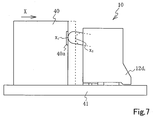
- Fig. 6 is a side view of the probe-type contact, and Fig. 7 is a side view showing the state of connection between the electric connector and equipment.
- An electric connector 10 is provided with a housing 11 having three through holes 13a to 13c, probe-type contacts 20a to 20c inserted into each through hole, and terminal portions 30a to 30c connected to each probe-type contact.
- the probe-type contacts 20a to 20c are constituted as follows. Pin-shaped contacts 22a to 22c are housed in conductive tubular bodies 21a to 21c in such manner as to move freely back and forth while being energized by springs (Fig. 3 shows only the spring 23a).
- the contacts are installed into the through holes 13a to 13c such that the tip portions of the probe-type contacts 20a to 20c are tilted upward at a predetermined angle in a horizontal direction, and the pin-shaped contacts 22a to 22c protrude from the surface of a front wall 12c of the housing 11.
- the housing 11 which is made of synthetic resin material consists of a cube having an upper wall 12a, a bottom wall 12b, a front wall 12c, a rear wall 12d, and right and left sidewalls 12e, 12f.
- the surface of the extended bottom wall 12b is made up of a plurality of supporting protrusions 12d 1 to 12d 4 that are integrally formed with the rear wall, and are provided on the rear wall surface at substantially equal gaps.
- the three through holes 13a to 13c penetrating from the rear wall 12d toward the front wall 12c surface are provided so as to be tilted upward from the rear wall 12d toward the front wall 12c surface at a predetermined angle in a horizontal direction.
- the tilt angle will be described in detail later.
- the through holes 13a to 13c are substantially circular in shape, and slits 14a to 14c of a narrow groove state are formed so as to communicate with the said through holes, extending to the bottom wall 12b.
- the through holes 13a to 13c are tilted at a predetermined angle in the horizontal direction so as to rise upward to the left from the rear wall 12d toward the front wall 12c. It is preferable that the tilt angle ⁇ be within the range of 6° to 15°.
- the pin-shaped contact hereinafter, referred to as a "pin contact" effectively wipes the surface of another terminal (the battery terminal, for example) when it contacts the surface of such other terminal.
- the diameter of the inner wall of the through holes 13a to 13c gradually becomes smaller from the rear wall 12d toward the front wall 12c.
- the diameter d 2 of the openings on the front wall 12c is smaller than the diameter d 1 of the openings on the rear wall 12d, but slightly larger than the diameter of the pin contact 22a, thereby not causing a problem in moving the pin contact 22a even if it contacts the inner wall of the through hole.
- the first, second and third steps 13a 1 , 13a 2 , 13a 3 are formed on the inner wall surface of the through hole 13a, and a tip step 21a 1 , a central step 21a 2 , and a rear step 21a 3 of the tubular body of the probe-type contact 20a are hooked, positioned and affixed to the steps 13a 1 , 13a 2 , 13a 3 respectively, thereby preventing the probe-type contact 20a from coming off from the through hole 13a.
- the other through holes 13b, 13c also have the same structure as the through hole 13a shown in the drawing, and each of the probe-type contacts 20b, 20c are likewise positioned and arranged in the same manner.
- the slits 14a to 14c communicating with the openings on the rear wall 12d are L-shaped and whose right and left sides are reversed, with a slit width formed slightly wider than the thickness of an interconnecting piece 32a that constitutes a portion of the terminal portion 30a. Then, the groove of the vertical portion of the L-shaped slit almost reaches the central area of the housing 11 from the rear wall 12d toward the front wall 12c, and a groove 14a 1 in the area close to the bottom wall 12b surface communicates from the rear wall 12d to the front wall 12c.
- the other slits 14b, 14c are similarly shaped.
- the housing 11 need not be in cubic form, as it may be of any shape. For example, it may be a plate-shaped body.
- the probe-type contacts 20a to 20c which are formed by metal of good conductivity, consist of the tubular bodies 21a to 21c having a predetermined diameter, the pin contacts 22a to 22c which are housed in the tubular bodies in such manner as to move freely and whose tips protrude from the front surface of the tubular bodies, and springs 23a to 23c (Fig. 3 illustrates only the spring 23) which are housed in the tubular bodies and energize the pin contacts so as to cause the contacts to protrude toward the front surface of the tubular bodies.
- the tip step 21a 1 , the central step 21a 2 , and the rear step 21a 3 are formed from the tip to the rear end of the tubular bodies 21a to 21c (Fig. 6 illustrates only the probe-type contact 20a), and the diameter of the central step 21a 2 is smaller than the diameter of the rear step 21a 3 .
- the other probe-type contacts 20b, 20c are similarly formed.
- the terminal portions 30a to 30c in the form of a plate-shaped body having good conductivity by bending process (Fig. 5(a) illustrates only the terminal portion 30a), are L-shaped whose right and left portions are substantially reversed.
- the terminal portion 30a consists of a circular contact 31a made up of the circular ring provided atop the L-shaped portion thereof, the interconnecting piece 32a that vertically comes down from the circular contact to a vertical portion, and terminal pieces 33a, 33a' at the bottom.
- the diameter of the ring of the circular contact 31a is substantially the same or slightly bigger than the diameter of the tubular body 21a of the probe-type contact 20a, which is designed in such manner that the circular contact 31a is pressed into the tubular body 21a and good electrical connection is thereby obtained by elastic force.
- each of the interconnecting pieces 32a, 32b and 32c extends in one direction at the bottom of the L-shaped part of the terminal portion, and a plurality of the connecting pieces 33a, 33a' are formed in a staggered manner to the right and left sides of the bottom of the extended area.
- a flat surface of a predetermined size is formed at the bottom surface of each of the connecting pieces 33a, 33a', designed to tightly contact the surface of the circuit board when it is mounted on the board.
- the connecting area with the wiring becomes wider when the connecting pieces are connected by soldering to the wiring on the circuit board, and therefore, good electrical connection is achieved.
- firm connection is attained which is useful for affixing the housing as well, eliminating the need to provide means for affixing the housing 11 onto the board.
- terminal portions 30a to 30c are L-shaped, the shape may be changed provided that the terminal pieces lead out to any direction from the top portion, right and left portions, and the rear portion. Further, the shape of the contact need not be circular and may be of any shape. Because the terminal portions can take any form, flexibility in creating their design is secured for purposes of installing them onto the circuit board or in the body of particular equipment.
- the three probe-type contacts 20a to 20c are inserted into the through holes 13a to 13c from the rear wall 12d of the housing 11 with the pins 22a to 22c facing forward.
- the tip step 21a 1 , the central step 21a 2 , and the rear step 21a 3 of the tubular bodies of the probe-type contacts 20a are hooked, positioned and affixed on the steps 13a 1 , 13a 2 , 13a 3 respectively, as shown in Fig. 4.
- the other probe-type contacts 20b, 20c are also inserted and affixed to the corresponding through holes 13b and 13c in the afore-described manner.
- the circular rings 31a to 31c of the corresponding terminal portions 30a to 30c are pushed into the through holes 13a to 13c and thereafter made to fit into the rear ends of the tubular bodies 21a to 21c of the probe-type contacts, and are thereby electrically connected to the tubular bodies.
- the interconnecting pieces 32a to 32c of the terminal portions 30a to 30c are pressed into the slits 14a to 14c and affixed thereto.
- the connecting pieces 33a, 33a', 33b, 33b', 33c, 33c' are arranged at the front, rear, right and left positions on the bottom wall surface 12b of the housing 11.
- connecting pieces 33a, 33a', 33b, 33b', 33c, 33c' are connected by soldering to the circuit wiring (not shown) of a circuit board 41 and thereby electrically connected thereto while the housing 11 is also affixed to the circuit board 41 at the same time.
- Fig. 7 shows the state in which the electric connector 10 is attached to the circuit board 41, and a battery component 40 is installed to the circuit board 41 via the electric connector 10.
- a battery terminal 40a contacts the pin contact 22a of the probe-type contact 20 in a horizontal direction marked by the arrow X.
- the contact position of the terminal 40a and the pin contact 22a is a contact point xi on the surface of the terminal.
- the pin contact 22a withdraws and recedes into the tubular body 21a resisting the energizing force of the spring, and the contact point of the pin contact 22a and the battery terminal 40a moves to x 2 due to the movement of the pin contact.
- the surface of the terminal 40a moves from the contact point x 1 to x 2 , and the contact point of the pin contact 22a rubs the terminal surface and wiping is performed. Because of the wiping action, oxide film and the like that may form on the surface of the terminal is peeled off, and good electrical connection is thereby achieved. Meanwhile, such wiping action similarly ensues in the other terminals 40b, 40c, obtaining the same effect.
- the electric connector 10 is supported by the supporting protrusion 12d 1 provided on the rear surface of the housing thereof even if strong force is applied from the front wall direction of the housing when the component such as a battery is installed, preventing the electric connector from being peeled off from the board 41.
Landscapes
- Measuring Leads Or Probes (AREA)
- Coupling Device And Connection With Printed Circuit (AREA)
Abstract
Description
- The present invention relates to an electric connector, more particularly to the modification of an electric connector using a contact(s) where a pin-shaped contact(s) is housed in a conductive tubular body (bodies) in such manner that the contact(s) is energized to move freely back and forth by a spring(s), which is a so-called probe-type contact.
- First, an electric connector using a conventional probe-type joint will be described using a drawing. Fig. 8 shows the electric connector using the probe-type contact described in Japanese Patent Laid-Open Publication No. 11-149954 publication (Refer to Fig. 6, right column on
page 3.), in which Figs. (a) and (b) respectively show the sectional view of the contact and the side view showing the state of connection of the electric connector with particular equipment. - In the probe-
type contact 2, as shown in Fig. 8, aconductive pin 3 is arranged in such manner as to move freely in protruding and withdrawing directions in aconductive tube 4, and a narrow portion is provided at the tip of theconductive tube 4 to prevent theconductive pin 3 from coming out in the protruding direction. Further, acoil spring 5 is provided in a retracted state in theconductive tube 4 so as to elastically energize theconductive pin 3 in the protruding direction. - The probe-
type contact 2 constituted in this manner is electrically connected to a circuit board 6 in an electric connector main body 1 of a cell phone and the like as shown in Fig. 8. On the other hand, abattery 7 is installed to the electric connector main body 1 in such manner as to be freely detachable. Then, theconductive pin 3 elastically contacts theterminal 7a of thebattery 7 in an attached state and thus the electric connector main body 1 and thebattery 7 are electrically connected via theterminal 7a and the probe-type contact 2. - The
battery 7 is attached to the electric connector main body 1 when theterminal 7a of thebattery 7 contacts the contact of theconductive pin 3 of the probe-type contact 2 in a horizontal direction marked by the arrow X. At this point, the contact position of theterminal 7a and theconductive pin 3 is a contact point x0 on the surface of theterminal 7a, and when the battery is moved further in the direction of X, theconductive pin 3 withdraws and recedes into theconductive tube 4 resisting the energizing force of thespring 5. Such movement of theconductive pin 3 causes its tip portion to elastically contact thebattery terminal 7a, and its contact point x'0 is at the same position as the point before the move. - However, there are cases where dust and the like adheres to or an oxide film is formed on the terminal surface of the battery, causing contact failure, thereby preventing good electrical connection.
- The present invention aims to solve the abovementioned problem of the prior art, and the first object of the present invention is to provide an electric connector in which contact failure does not occur in a connector using a probe-type contact.
- Further, the second object of the present invention is to provide an electric connector that can be firmly affixed onto a circuit board.
- The aforestated objects of the present invention can be achieved by the following constitutions. Specifically, the invention of the electric connector according to Claim 1 of the present invention is characterized in that it is provided with a housing having at least one through hole, a probe-type contact(s) inserted into the through hole(s); and a terminal portion(s) connected to the probe-type contact(s), in which the probe-type contact is such that a pin-shaped contact is housed in a conductive tubular body in such manner as to move freely while being energized by a spring, and the pin-shaped contact at the tip of the contact is tilted upward at a predetermined angle in a horizontal direction and installed into the through hole so as to protrude from the front wall surface of the housing.
- Further, the invention according to
Claim 2 of the present invention is the electric connector according to Claim 1, in which the predetermined angle is in the range of 6° to 15°. - Furthermore, the invention according to
Claim 3 of the present invention is the electric connector according to Claim 1, in which the terminal portion having a contact on one end and a terminal on the other end and is formed by conductive metal plate, and the contact is connected to the tubular body of the probe-type contact. - Further, Furthermore, the invention according to
Claim 4 of the present invention is the electric connector according to Claim 1, in which the terminal portion, which is formed by a conductive metal plate, being substantially L-shaped and consisting of a contact residing atop the L-shape part thereof, an interconnecting piece at its vertical part, and a terminal at its bottom part. - Further, the invention according to
Claim 5 of the present invention is the electric connector according toClaims - Furthermore, the invention according to Claim 6 of the present invention is the electric connector according to
Claim 5, in which the contact of the terminal portion is made of a circular ring, and the circular ring is connected as to fit into the said tubular body of the probe-type contact. - Further, the invention according to
Claim 7 of the present invention is the electric connector according toClaims - Further, the invention according to Claim 8 of the present invention is the electric connector according to Claim 1, in which the housing has a plurality of supporting protrusions jutting outward at the bottom portion of the rear side in the direction where the pin-shaped contact is protruded.
- The above-described constitution of the present invention exhibits the following features. Specifically, according to the electric connector of the present invention, when a component such as a battery is attached to the electric connector that is built into electronic equipment such as a cell phone, the pin-shaped contact of the probe-type contact abuts the terminal of the battery and the like, and the pin-shaped contact withdraws into the tubular body resisting the repulsion of the spring. At the point of withdrawal, the contact point of the pin-shaped contact and the terminal of the battery and the like moves, allowing the pin-shaped contact to rub the surface of the terminal over a predetermined range, which is referred to as a "wiping action". Therefore, in the electric connector of the present invention, even if contamination adheres to the surface of the terminal or an oxide film and the like is formed thereon, the wiping action rubs them off and good electrical connection is achieved.
- Further, according to the electric connector of another mode of the present invention, good wiping action can be achieved by selecting the predetermined angle from within the range of 6° to 15°. In addition, since a plurality of supporting protrusions are provided on the lower wall portion on the rear side of the housing, the supporting protrusions abut on the circuit board surface even when the terminal of the battery and the like pushes the pin-shaped contact when force is applied, making the housing draw away from the circuit board, thereby preventing the housing from being peeled off from the circuit board.
- Furthermore, according to the electric connector of another mode of the present invention, the terminal portion is separated from the probe-type contact, which facilitates the design and manufacturing of both components. Additionally, since various types of separate connecting portions can be formed, it is possible to draw out the terminal from the housing in any direction (whether upward, downward, rightward, leftward or rearward), thereby increasing flexibility in creating the layout design of equipment for mounting the electric connector.
- Further still, according to the electric connector of another mode of the present invention, the contact is connected to the tubular body of the probe-type contact in such manner as to be freely detachable, making for easier assembly and allowing replacement of components as well as facilitating repair. Moreover, since the contact is made of a circular ring, attachment or detachment thereof from the probe-type contact becomes effortless.
- Further, according to the electric connector of another mode of the present invention, connection with the circuit board can be achieved by a plurality of the connecting pieces provided at the L-shaped base in a staggered state. Therefore, the number of connecting points is increased, and even if connection failure occurs on one connecting piece, the existence of other connecting pieces practically eliminates the occurrence of almost all connection failures. In addition, the connection made by the connecting pieces serves as the mode of attaching of the connector housing to the circuit board, and therefore providing means for affixing the housing is not necessary.
- Further, according to the electric connector of another mode of the present invention, since the terminal portion is substantially L-shaped, it is possible to draw out the terminal to the lower wall surface of housing. Additionally, by mounting the lower wall surface of the housing on the circuit board and connecting the terminal to the circuit wiring of circuit board by soldering, the housing can be affixed to the circuit board without providing the means therefor.
-
- Fig. 1 is a perspective of the external view of the electric connector of the present invention.
- Fig. 2 is a bottom surface view of the electric connector.
- Fig. 3 is an exploded view of the electric connector of Fig. 1.
- Fig. 4 is a sectional view at A-A of Fig. 1.
- Figs. 5 (a), (b) and (c) respectively show the front, right side and bottom surface views of the terminal portion of Fig. 3.
- Fig. 6 is a side view of the probe-type contact.
- Fig. 7 is a side view showing the state of connection between the electric connector and equipment.
- Figs. 8 (a) and (b) show an electric connector using a probe-type contact of the prior art, where Fig. 8(a) is the sectional view of the contact, and Fig. 8(b) is the side view showing the state of connection thereof with particular equipment.
-
- The preferred embodiments of the present invention will hereafter be described with reference to the drawings. Note that while the embodiments described below exemplify the technical essence of the present invention, the same embodiments are not confined to the present invention as the other embodiments included in the claims equally apply to the present invention.
- Fig. 1 is a perspective of the external view of the electric connector of the present invention, while Fig. 2 is the bottom surface view of the electric connector and Fig. 3 is an exploded view of the electric connector shown in Fig. 1. Fig. 4 is the sectional view at A-A of Fig. 1, while Figs. 5 (a), (b) and (c) respectively show the front, right side and bottom surface views of the terminal portion of Fig. 3. Fig. 6 is a side view of the probe-type contact, and Fig. 7 is a side view showing the state of connection between the electric connector and equipment.
- An
electric connector 10 is provided with ahousing 11 having three throughholes 13a to 13c, probe-type contacts 20a to 20c inserted into each through hole, andterminal portions 30a to 30c connected to each probe-type contact. The probe-type contacts 20a to 20c are constituted as follows. Pin-shaped contacts 22a to 22c are housed in conductivetubular bodies 21a to 21c in such manner as to move freely back and forth while being energized by springs (Fig. 3 shows only thespring 23a). The contacts are installed into the throughholes 13a to 13c such that the tip portions of the probe-type contacts 20a to 20c are tilted upward at a predetermined angle in a horizontal direction, and the pin-shaped contacts 22a to 22c protrude from the surface of afront wall 12c of thehousing 11. - Each member that constitutes the
electric connector 10 will be described next. - As shown in Fig. 3, the
housing 11 which is made of synthetic resin material consists of a cube having anupper wall 12a, abottom wall 12b, afront wall 12c, arear wall 12d, and right andleft sidewalls - A part of the
bottom wall 12b surface extends backward on therear wall 12d side. As shown in Fig. 2, the surface of theextended bottom wall 12b is made up of a plurality of supportingprotrusions 12d1 to 12d4 that are integrally formed with the rear wall, and are provided on the rear wall surface at substantially equal gaps. - Further, in the
housing 11, the three throughholes 13a to 13c penetrating from therear wall 12d toward thefront wall 12c surface are provided so as to be tilted upward from therear wall 12d toward thefront wall 12c surface at a predetermined angle in a horizontal direction. The tilt angle will be described in detail later. - The through
holes 13a to 13c are substantially circular in shape, and slits 14a to 14c of a narrow groove state are formed so as to communicate with the said through holes, extending to thebottom wall 12b. - The through
holes 13a to 13c (Fig. 4 illustrates only the throughhole 13a) are tilted at a predetermined angle in the horizontal direction so as to rise upward to the left from therear wall 12d toward thefront wall 12c. It is preferable that the tilt angle be within the range of 6° to 15°. When the tilt angle is selected from the aforeprescribed range and the probe-type contact is installed to each through hole, the pin-shaped contact (hereinafter, referred to as a "pin contact") effectively wipes the surface of another terminal (the battery terminal, for example) when it contacts the surface of such other terminal. - Furthermore, the diameter of the inner wall of the through
holes 13a to 13c gradually becomes smaller from therear wall 12d toward thefront wall 12c. The diameter d2 of the openings on thefront wall 12c is smaller than the diameter d1 of the openings on therear wall 12d, but slightly larger than the diameter of thepin contact 22a, thereby not causing a problem in moving thepin contact 22a even if it contacts the inner wall of the through hole. - Further, as shown in Figs. 4 and 6, the first, second and
third steps hole 13a, and atip step 21a1, acentral step 21a2, and arear step 21a3 of the tubular body of the probe-type contact 20a are hooked, positioned and affixed to thesteps type contact 20a from coming off from the throughhole 13a. The other throughholes hole 13a shown in the drawing, and each of the probe-type contacts - The
slits 14a to 14c communicating with the openings on therear wall 12d (Fig. 4 shows only theslit 14a) are L-shaped and whose right and left sides are reversed, with a slit width formed slightly wider than the thickness of aninterconnecting piece 32a that constitutes a portion of theterminal portion 30a. Then, the groove of the vertical portion of the L-shaped slit almost reaches the central area of thehousing 11 from therear wall 12d toward thefront wall 12c, and agroove 14a1 in the area close to thebottom wall 12b surface communicates from therear wall 12d to thefront wall 12c. Theother slits housing 11 need not be in cubic form, as it may be of any shape. For example, it may be a plate-shaped body. - The probe-
type contacts 20a to 20c which are formed by metal of good conductivity, consist of thetubular bodies 21a to 21c having a predetermined diameter, thepin contacts 22a to 22c which are housed in the tubular bodies in such manner as to move freely and whose tips protrude from the front surface of the tubular bodies, and springs 23a to 23c (Fig. 3 illustrates only the spring 23) which are housed in the tubular bodies and energize the pin contacts so as to cause the contacts to protrude toward the front surface of the tubular bodies. - Of varying diameters, the
tip step 21a1, thecentral step 21a2, and therear step 21a3 are formed from the tip to the rear end of thetubular bodies 21a to 21c (Fig. 6 illustrates only the probe-type contact 20a), and the diameter of thecentral step 21a2 is smaller than the diameter of therear step 21a3. The other probe-type contacts - When the
pin contact 22a of the probe-type contact is pushed by the terminal of the battery and the like, the pin contact withdraws, resisting the energizing force of the spring, thereby elastically contacting the terminal by virtue of the spring, and a state of good electrical connection is maintained. - The
terminal portions 30a to 30c, in the form of a plate-shaped body having good conductivity by bending process (Fig. 5(a) illustrates only theterminal portion 30a), are L-shaped whose right and left portions are substantially reversed. - The
terminal portion 30a consists of acircular contact 31a made up of the circular ring provided atop the L-shaped portion thereof, the interconnectingpiece 32a that vertically comes down from the circular contact to a vertical portion, andterminal pieces circular contact 31a is substantially the same or slightly bigger than the diameter of thetubular body 21a of the probe-type contact 20a, which is designed in such manner that thecircular contact 31a is pressed into thetubular body 21a and good electrical connection is thereby obtained by elastic force. - Further, the bottom end of each of the interconnecting
pieces pieces - A flat surface of a predetermined size is formed at the bottom surface of each of the connecting
pieces - Since a plurality of the connecting
pieces housing 11 onto the board. - Meanwhile, although the
terminal portions 30a to 30c are L-shaped, the shape may be changed provided that the terminal pieces lead out to any direction from the top portion, right and left portions, and the rear portion. Further, the shape of the contact need not be circular and may be of any shape. Because the terminal portions can take any form, flexibility in creating their design is secured for purposes of installing them onto the circuit board or in the body of particular equipment. - The assembly method of fitting the contact to the housing will be described hereafter.
- The three probe-
type contacts 20a to 20c are inserted into the throughholes 13a to 13c from therear wall 12d of thehousing 11 with thepins 22a to 22c facing forward. In this manner, thetip step 21a1, thecentral step 21a2, and therear step 21a3 of the tubular bodies of the probe-type contacts 20a are hooked, positioned and affixed on thesteps type contacts holes - Subsequently, the
circular rings 31a to 31c of the correspondingterminal portions 30a to 30c are pushed into the throughholes 13a to 13c and thereafter made to fit into the rear ends of thetubular bodies 21a to 21c of the probe-type contacts, and are thereby electrically connected to the tubular bodies. At the same time, the interconnectingpieces 32a to 32c of theterminal portions 30a to 30c are pressed into theslits 14a to 14c and affixed thereto. In this manner, the connectingpieces bottom wall surface 12b of thehousing 11. Thereafter, the connectingpieces housing 11 is also affixed to the circuit board 41 at the same time. - Fig. 7 shows the state in which the
electric connector 10 is attached to the circuit board 41, and abattery component 40 is installed to the circuit board 41 via theelectric connector 10. When thebattery component 40 is connected to theelectric connector 10, abattery terminal 40a contacts thepin contact 22a of the probe-type contact 20 in a horizontal direction marked by the arrow X. At this point, the contact position of the terminal 40a and thepin contact 22a is a contact point xi on the surface of the terminal. When the battery is moved further in the direction of X, thepin contact 22a withdraws and recedes into thetubular body 21a resisting the energizing force of the spring, and the contact point of thepin contact 22a and thebattery terminal 40a moves to x2 due to the movement of the pin contact. Concurrently, the surface of the terminal 40a moves from the contact point x1 to x2, and the contact point of thepin contact 22a rubs the terminal surface and wiping is performed. Because of the wiping action, oxide film and the like that may form on the surface of the terminal is peeled off, and good electrical connection is thereby achieved. Meanwhile, such wiping action similarly ensues in the other terminals 40b, 40c, obtaining the same effect. - Furthermore, the
electric connector 10 is supported by the supportingprotrusion 12d1 provided on the rear surface of the housing thereof even if strong force is applied from the front wall direction of the housing when the component such as a battery is installed, preventing the electric connector from being peeled off from the board 41. - The features disclosed in the foregoing description, in the claims and/or in the accompanying drawings may, both separately and in any combination thereof, be material for realising the invention in diverse forms thereof.
Claims (8)
- An electric connector, comprising:wherein the probe-type contact consists of a pin-shaped contact housed in a conductive tubular body in such manner as to move freely while being energized by a spring, and the tip of the pin-shaped contact being tilted upward at a predetermined angle in a horizontal direction and installed into the through hole so as to protrude from the front wall surface of the housing.a housing having at least one through hole,a probe-type contact(s) inserted into the through hole(s); anda terminal portion(s) connected to the probe-type contact(s),
- The electric connector according to Claim 1, wherein the said predetermined angle is within the range of 6° to 15°.
- The electric connector according to Claim 1, wherein the said terminal portion having a contact on one end and a terminal on the other end and is formed by conductive metal plate, and the contact is connected to the tubular body of said probe-type contact.
- The electric connector according to Claim 1, wherein the said terminal portion, which is formed by a conductive metal plate, being substantially L-shaped and consisting of a contact residing atop the L-shape part thereof, an interconnecting piece at its vertical part, and a terminal at its bottom part.
- The electric connector according to Claims 3 or 4, wherein the contact of said terminal portion is connected to the tubular body of said probe-type contact in such manner as to be freely detachable.
- The electric connector according to Claim 5, wherein the contact of said terminal portion is made of a circular ring, and the circular ring is connected as to fit into the said tubular body of the probe-type contact.
- The electric connector according to Claims 3 or 4, wherein the terminal of said terminal portion is at an L-shaped base and at least two connecting pieces are alternately disposed at the front and rear sides and to the right and left sides of the base in a staggered state.
- The electric connector according to Claim 1, wherein the said housing has a plurality of supporting protrusions jutting outward at the bottom portion of the rear side in the direction where said pin-shaped contact is protruded.
Applications Claiming Priority (2)
| Application Number | Priority Date | Filing Date | Title |
|---|---|---|---|
| JP2003283260A JP2005050738A (en) | 2003-07-31 | 2003-07-31 | Electrical connector |
| JP2003283260 | 2003-07-31 |
Publications (2)
| Publication Number | Publication Date |
|---|---|
| EP1503458A1 true EP1503458A1 (en) | 2005-02-02 |
| EP1503458B1 EP1503458B1 (en) | 2014-06-18 |
Family
ID=33535695
Family Applications (1)
| Application Number | Title | Priority Date | Filing Date |
|---|---|---|---|
| EP04018104.2A Expired - Lifetime EP1503458B1 (en) | 2003-07-31 | 2004-07-30 | Electric connector |
Country Status (6)
| Country | Link |
|---|---|
| US (1) | US6935906B2 (en) |
| EP (1) | EP1503458B1 (en) |
| JP (1) | JP2005050738A (en) |
| KR (1) | KR101083209B1 (en) |
| CN (1) | CN100483854C (en) |
| TW (1) | TWI322537B (en) |
Cited By (2)
| Publication number | Priority date | Publication date | Assignee | Title |
|---|---|---|---|---|
| WO2009011463A3 (en) * | 2007-07-19 | 2009-05-14 | Yokowo Seisakusho Kk | Right angle type spring connector |
| TWI392154B (en) * | 2008-09-08 | 2013-04-01 | Hon Hai Prec Ind Co Ltd | Electrical connector |
Families Citing this family (41)
| Publication number | Priority date | Publication date | Assignee | Title |
|---|---|---|---|---|
| CN2682639Y (en) * | 2003-11-20 | 2005-03-02 | 上海莫仕连接器有限公司 | Crimp connected conductive terminal |
| JP4224389B2 (en) * | 2003-12-16 | 2009-02-12 | 株式会社ヨコオ | Spring connector |
| JP2005302432A (en) * | 2004-04-08 | 2005-10-27 | Citizen Electronics Co Ltd | Spring connector |
| US7255572B2 (en) * | 2005-08-31 | 2007-08-14 | Yokowo Co., Ltd. | Electrical connector provided with coiled spring contact |
| FR2901066A1 (en) * | 2006-05-15 | 2007-11-16 | Radiall Sa | COAXIAL CONNECTOR |
| US20080126194A1 (en) * | 2006-11-28 | 2008-05-29 | The Adason Group, Llc | Methods for advertising in airport and/or seaport security areas |
| TWM324906U (en) * | 2007-07-20 | 2008-01-01 | Advanced Connectek Inc | Electrical connector |
| WO2009128144A1 (en) * | 2008-04-16 | 2009-10-22 | 三菱電機株式会社 | Functional unit for disc device and disc device |
| US7942705B2 (en) * | 2009-03-20 | 2011-05-17 | Apple Inc. | Audio jack with pogo pins for conductive contacts |
| CN101562282B (en) * | 2009-05-19 | 2011-01-19 | 宁波高正电子有限公司 | Electric connector |
| US7789719B1 (en) * | 2009-06-29 | 2010-09-07 | Cheng Uei Precision Industry Co., Ltd. | Probe connector |
| US7815474B1 (en) * | 2009-08-28 | 2010-10-19 | Cheng Uei Precision Industry Co., Ltd. | Probe connector having a mounting platform |
| US8419479B2 (en) * | 2009-09-17 | 2013-04-16 | Matthew Leigh Vroom | Docking station for an electronic device with improved electrical interface |
| US9285831B2 (en) | 2009-09-17 | 2016-03-15 | Henge Docks Llc | Docking station for portable electronics |
| US20110111643A1 (en) * | 2009-11-07 | 2011-05-12 | Yin Te-Hung | Audio Connector |
| US8215006B2 (en) * | 2009-11-26 | 2012-07-10 | Cheng Uei Precision Industry Co., Ltd. | Jig for probe connector |
| US20110138612A1 (en) * | 2009-12-10 | 2011-06-16 | Yin Te-Hung | Jig For Probe Connector |
| US7914348B1 (en) * | 2010-06-15 | 2011-03-29 | Cheng Uei Precision Industry Co., Ltd. | Probe connector |
| US20110318944A1 (en) * | 2010-06-28 | 2011-12-29 | Ming-Han Lin | Probe Connector |
| US8272903B2 (en) * | 2011-02-15 | 2012-09-25 | Cheng Uei Precision Industry Co., Ltd. | Probe connector |
| US8491338B1 (en) * | 2012-05-23 | 2013-07-23 | Proconn Technology Co., Ltd. | Battery connector |
| CN103364750A (en) * | 2013-06-27 | 2013-10-23 | 曙光信息产业(北京)有限公司 | Auxiliary device for calibration of oscilloscope and calibration method |
| TWI500222B (en) * | 2013-07-12 | 2015-09-11 | Ccp Contact Probes Co Ltd | Connector combination |
| US9011184B2 (en) * | 2013-08-23 | 2015-04-21 | Cheng Uei Precision Industry Co., Ltd. | Pogo pin connector |
| US9927838B2 (en) | 2013-12-31 | 2018-03-27 | Henge Docks Llc | Sensor system for docking station |
| US9650814B2 (en) | 2013-12-31 | 2017-05-16 | Henge Docks Llc | Alignment and drive system for motorized horizontal docking station |
| US10018514B2 (en) * | 2014-02-17 | 2018-07-10 | Haier Us Appliance Solutions, Inc. | Cooktop temperature sensors and methods of operation |
| US9887478B2 (en) * | 2015-04-21 | 2018-02-06 | Varian Semiconductor Equipment Associates, Inc. | Thermally insulating electrical contact probe |
| US9727084B2 (en) | 2015-10-23 | 2017-08-08 | Henge Docks Llc | Drivetrain for a motorized docking station |
| US9575510B1 (en) | 2015-10-23 | 2017-02-21 | Matthew Leigh Vroom | Precision docking station for an electronic device having integrated retention mechanism |
| US9811118B2 (en) | 2015-10-23 | 2017-11-07 | Henge Docks Llc | Secure assembly for a docking station |
| CN105449414A (en) * | 2015-12-29 | 2016-03-30 | 中物功能材料研究院有限公司 | Scalable contact conductive connection device |
| CN105742859A (en) * | 2016-04-08 | 2016-07-06 | 黄永怀 | Columnar electrical connector |
| US9882301B1 (en) * | 2016-09-30 | 2018-01-30 | General Electric Company | Current restrictive spring-loaded electrical connection device |
| US9647367B1 (en) * | 2016-09-30 | 2017-05-09 | General Electric Company | Current restrictive spring-loaded electrical connection device |
| TWI620893B (en) * | 2016-10-26 | 2018-04-11 | Luminescence Technology Corporation | OLED planar light source module |
| CN107706565A (en) * | 2017-08-16 | 2018-02-16 | 深圳天珑无线科技有限公司 | A kind of electric connector |
| US10365688B1 (en) | 2018-04-19 | 2019-07-30 | Henge Docks Llc | Alignment sleeve for docking station |
| CN109066153B (en) * | 2018-07-25 | 2020-04-10 | 深圳市爱默斯科技有限公司 | Connector for electrical applications |
| CN112510479A (en) * | 2020-12-02 | 2021-03-16 | 南昌攀藤科技有限公司 | Laser device |
| CN117748196A (en) * | 2022-09-14 | 2024-03-22 | 北京车和家信息技术有限公司 | PIN PIN male end, PIN PIN female end and connector |
Citations (1)
| Publication number | Priority date | Publication date | Assignee | Title |
|---|---|---|---|---|
| EP1253674A2 (en) | 2001-04-27 | 2002-10-30 | Yokowo Co., Ltd. | Spring connector |
Family Cites Families (25)
| Publication number | Priority date | Publication date | Assignee | Title |
|---|---|---|---|---|
| US2724096A (en) * | 1952-12-04 | 1955-11-15 | American Phenolic Corp | Spring loaded butt contact with internal contacting sleeve |
| US3771110A (en) * | 1971-11-23 | 1973-11-06 | Walton Prod Inc | Electrical contact pins |
| US4281888A (en) * | 1979-09-07 | 1981-08-04 | Western Electric Company, Inc. | Apparatus for testing leads of fuse holders |
| US4342497A (en) * | 1979-09-07 | 1982-08-03 | National Motor Spares Corporation | Battery terminal connector |
| US4508405A (en) * | 1982-04-29 | 1985-04-02 | Augat Inc. | Electronic socket having spring probe contacts |
| JPS61181060A (en) * | 1985-02-04 | 1986-08-13 | チヤ−ルズ ア−チヤ− モ−リソン | Battery terminal connector |
| US4904213A (en) * | 1989-04-06 | 1990-02-27 | Motorola, Inc. | Low impedance electric connector |
| JPH0412483A (en) * | 1990-04-27 | 1992-01-17 | Kel Corp | Ic socket |
| JPH05182729A (en) * | 1991-12-26 | 1993-07-23 | Yamaichi Electron Co Ltd | Contactor for electrical parts |
| CA2114813A1 (en) * | 1994-02-02 | 1995-08-03 | Sing-Long Du | Transmission power testing bar of cable television system |
| US5643016A (en) * | 1995-07-28 | 1997-07-01 | The Whitaker Corporation | Electrical connector assembly with contact retention and removal system |
| US5641315A (en) * | 1995-11-16 | 1997-06-24 | Everett Charles Technologies, Inc. | Telescoping spring probe |
| US5667410A (en) * | 1995-11-21 | 1997-09-16 | Everett Charles Technologies, Inc. | One-piece compliant probe |
| JP2899585B1 (en) * | 1998-03-18 | 1999-06-02 | エスエムケイ株式会社 | Connector terminal structure |
| US5980335A (en) * | 1998-03-27 | 1999-11-09 | Molex Incorporated | Electrical terminal |
| JP2000182701A (en) * | 1998-12-18 | 2000-06-30 | Honda Tsushin Kogyo Co Ltd | Probe pin, manufacturing method thereof and connector |
| US6083059A (en) * | 1999-05-28 | 2000-07-04 | Ant Precision Industry Co., Ltd. | Structure of a terminal |
| KR100373152B1 (en) * | 1999-11-17 | 2003-02-25 | 가부시키가이샤 아드반테스트 | Ic socket and ic testing apparatus |
| IT1317517B1 (en) * | 2000-05-11 | 2003-07-09 | Technoprobe S R L | MEASUREMENT HEAD FOR MICROSTRUCTURES |
| US6663439B2 (en) * | 2001-03-02 | 2003-12-16 | Tyco Electronics Corporation | Electrical connector with spring biased contacts |
| US6604864B2 (en) * | 2001-04-17 | 2003-08-12 | Itt Manufacturing Enterprises, Inc. | Optic fiber connector spring retainer |
| TW549662U (en) * | 2001-06-08 | 2003-08-21 | Hon Hai Prec Ind Co Ltd | Electrical connector |
| US20040077225A1 (en) * | 2002-10-21 | 2004-04-22 | L & K Precision Industry Co., Ltd. | Electrical connector with movable pin |
| US6758682B1 (en) * | 2003-02-13 | 2004-07-06 | Itt Manufacturing Enterprises, Inc. | Pogo contact |
| US6776668B1 (en) * | 2003-08-01 | 2004-08-17 | Tyco Electronics Corporation | Low profile coaxial board-to-board connector |
-
2003
- 2003-07-31 JP JP2003283260A patent/JP2005050738A/en not_active Withdrawn
-
2004
- 2004-07-28 CN CNB2004100710825A patent/CN100483854C/en not_active Expired - Fee Related
- 2004-07-28 US US10/900,379 patent/US6935906B2/en not_active Expired - Fee Related
- 2004-07-29 TW TW093122645A patent/TWI322537B/en not_active IP Right Cessation
- 2004-07-29 KR KR1020040059517A patent/KR101083209B1/en not_active Expired - Fee Related
- 2004-07-30 EP EP04018104.2A patent/EP1503458B1/en not_active Expired - Lifetime
Patent Citations (1)
| Publication number | Priority date | Publication date | Assignee | Title |
|---|---|---|---|---|
| EP1253674A2 (en) | 2001-04-27 | 2002-10-30 | Yokowo Co., Ltd. | Spring connector |
Cited By (3)
| Publication number | Priority date | Publication date | Assignee | Title |
|---|---|---|---|---|
| WO2009011463A3 (en) * | 2007-07-19 | 2009-05-14 | Yokowo Seisakusho Kk | Right angle type spring connector |
| US7909660B2 (en) | 2007-07-19 | 2011-03-22 | Yokowo Co., Ltd. | Right angle type spring connector |
| TWI392154B (en) * | 2008-09-08 | 2013-04-01 | Hon Hai Prec Ind Co Ltd | Electrical connector |
Also Published As
| Publication number | Publication date |
|---|---|
| KR101083209B1 (en) | 2011-11-11 |
| KR20050014698A (en) | 2005-02-07 |
| US20050026510A1 (en) | 2005-02-03 |
| US6935906B2 (en) | 2005-08-30 |
| TW200514306A (en) | 2005-04-16 |
| TWI322537B (en) | 2010-03-21 |
| EP1503458B1 (en) | 2014-06-18 |
| CN100483854C (en) | 2009-04-29 |
| CN1581592A (en) | 2005-02-16 |
| JP2005050738A (en) | 2005-02-24 |
Similar Documents
| Publication | Publication Date | Title |
|---|---|---|
| EP1503458B1 (en) | Electric connector | |
| US7140896B2 (en) | Connector | |
| US7374430B2 (en) | Electrical connector for connecting a flat-type circuit board | |
| US7094093B2 (en) | Connector | |
| KR100330863B1 (en) | Coaxial Connector | |
| US7635274B2 (en) | Electrical connector | |
| JP4210725B2 (en) | Electronic device module socket and electronic device module | |
| KR20180077069A (en) | Electric connector | |
| CN101997197B (en) | Connector | |
| US6022248A (en) | Connecting terminal having enhanced biasing force | |
| JP5258543B2 (en) | connector | |
| US7147477B2 (en) | High density electrical connector | |
| US7753736B2 (en) | Electrical connector confitured by upper and lower units | |
| US7437929B2 (en) | Liquid level detector | |
| JP2004172128A (en) | Double contact electric compression connector | |
| US7059883B2 (en) | Electrical connector capable of moving a circuit board in a reverse direction to an inserting direction by a distance | |
| US7341470B2 (en) | Electrical connector for flexible printed circuit boards | |
| US20030141174A1 (en) | Electronic device switch | |
| CN115997322B (en) | Connector with a plurality of connectors | |
| JP2002329540A (en) | Press-fit type connector for mobile phone and its connection structure | |
| JP4530887B2 (en) | connector | |
| JP5735400B2 (en) | Cover with click elastic contact body and manufacturing method thereof | |
| JP2010055774A (en) | Fpc connector | |
| KR200254993Y1 (en) | Electrical connector using elestomer polymer board | |
| CN119297635A (en) | A substrate connector |
Legal Events
| Date | Code | Title | Description |
|---|---|---|---|
| PUAI | Public reference made under article 153(3) epc to a published international application that has entered the european phase |
Free format text: ORIGINAL CODE: 0009012 |
|
| AK | Designated contracting states |
Kind code of ref document: A1 Designated state(s): AT BE BG CH CY CZ DE DK EE ES FI FR GB GR HU IE IT LI LU MC NL PL PT RO SE SI SK TR |
|
| AX | Request for extension of the european patent |
Extension state: AL HR LT LV MK |
|
| 17P | Request for examination filed |
Effective date: 20050307 |
|
| AKX | Designation fees paid |
Designated state(s): DE FI FR SE |
|
| 17Q | First examination report despatched |
Effective date: 20090402 |
|
| GRAJ | Information related to disapproval of communication of intention to grant by the applicant or resumption of examination proceedings by the epo deleted |
Free format text: ORIGINAL CODE: EPIDOSDIGR1 |
|
| GRAP | Despatch of communication of intention to grant a patent |
Free format text: ORIGINAL CODE: EPIDOSNIGR1 |
|
| GRAP | Despatch of communication of intention to grant a patent |
Free format text: ORIGINAL CODE: EPIDOSNIGR1 |
|
| RIN1 | Information on inventor provided before grant (corrected) |
Inventor name: ORIHARA, MASAYUKI, |
|
| INTG | Intention to grant announced |
Effective date: 20140127 |
|
| GRAS | Grant fee paid |
Free format text: ORIGINAL CODE: EPIDOSNIGR3 |
|
| GRAA | (expected) grant |
Free format text: ORIGINAL CODE: 0009210 |
|
| AK | Designated contracting states |
Kind code of ref document: B1 Designated state(s): DE FI FR SE |
|
| REG | Reference to a national code |
Ref country code: DE Ref legal event code: R096 Ref document number: 602004045279 Country of ref document: DE Effective date: 20140731 |
|
| PG25 | Lapsed in a contracting state [announced via postgrant information from national office to epo] |
Ref country code: FI Free format text: LAPSE BECAUSE OF FAILURE TO SUBMIT A TRANSLATION OF THE DESCRIPTION OR TO PAY THE FEE WITHIN THE PRESCRIBED TIME-LIMIT Effective date: 20140618 |
|
| PGFP | Annual fee paid to national office [announced via postgrant information from national office to epo] |
Ref country code: DE Payment date: 20140724 Year of fee payment: 11 |
|
| PG25 | Lapsed in a contracting state [announced via postgrant information from national office to epo] |
Ref country code: SE Free format text: LAPSE BECAUSE OF FAILURE TO SUBMIT A TRANSLATION OF THE DESCRIPTION OR TO PAY THE FEE WITHIN THE PRESCRIBED TIME-LIMIT Effective date: 20140618 |
|
| PGFP | Annual fee paid to national office [announced via postgrant information from national office to epo] |
Ref country code: FR Payment date: 20140731 Year of fee payment: 11 |
|
| REG | Reference to a national code |
Ref country code: DE Ref legal event code: R097 Ref document number: 602004045279 Country of ref document: DE |
|
| PLBE | No opposition filed within time limit |
Free format text: ORIGINAL CODE: 0009261 |
|
| STAA | Information on the status of an ep patent application or granted ep patent |
Free format text: STATUS: NO OPPOSITION FILED WITHIN TIME LIMIT |
|
| 26N | No opposition filed |
Effective date: 20150319 |
|
| REG | Reference to a national code |
Ref country code: DE Ref legal event code: R119 Ref document number: 602004045279 Country of ref document: DE |
|
| PG25 | Lapsed in a contracting state [announced via postgrant information from national office to epo] |
Ref country code: DE Free format text: LAPSE BECAUSE OF NON-PAYMENT OF DUE FEES Effective date: 20160202 |
|
| REG | Reference to a national code |
Ref country code: FR Ref legal event code: ST Effective date: 20160331 |
|
| PG25 | Lapsed in a contracting state [announced via postgrant information from national office to epo] |
Ref country code: FR Free format text: LAPSE BECAUSE OF NON-PAYMENT OF DUE FEES Effective date: 20150731 |