EP1501161A1 - Diode à cavité résonante, fonctionnant à la même longueur d'onde pour l'émission et la détection de lumière - Google Patents
Diode à cavité résonante, fonctionnant à la même longueur d'onde pour l'émission et la détection de lumière Download PDFInfo
- Publication number
- EP1501161A1 EP1501161A1 EP04103435A EP04103435A EP1501161A1 EP 1501161 A1 EP1501161 A1 EP 1501161A1 EP 04103435 A EP04103435 A EP 04103435A EP 04103435 A EP04103435 A EP 04103435A EP 1501161 A1 EP1501161 A1 EP 1501161A1
- Authority
- EP
- European Patent Office
- Prior art keywords
- cavity
- diode
- mirrors
- light
- vcsel
- Prior art date
- Legal status (The legal status is an assumption and is not a legal conclusion. Google has not performed a legal analysis and makes no representation as to the accuracy of the status listed.)
- Granted
Links
Images

Classifications
-
- H—ELECTRICITY
- H01—ELECTRIC ELEMENTS
- H01S—DEVICES USING THE PROCESS OF LIGHT AMPLIFICATION BY STIMULATED EMISSION OF RADIATION [LASER] TO AMPLIFY OR GENERATE LIGHT; DEVICES USING STIMULATED EMISSION OF ELECTROMAGNETIC RADIATION IN WAVE RANGES OTHER THAN OPTICAL
- H01S5/00—Semiconductor lasers
- H01S5/10—Construction or shape of the optical resonator, e.g. extended or external cavity, coupled cavities, bent-guide, varying width, thickness or composition of the active region
- H01S5/18—Surface-emitting [SE] lasers, e.g. having both horizontal and vertical cavities
- H01S5/183—Surface-emitting [SE] lasers, e.g. having both horizontal and vertical cavities having only vertical cavities, e.g. vertical cavity surface-emitting lasers [VCSEL]
- H01S5/18308—Surface-emitting [SE] lasers, e.g. having both horizontal and vertical cavities having only vertical cavities, e.g. vertical cavity surface-emitting lasers [VCSEL] having a special structure for lateral current or light confinement
- H01S5/18311—Surface-emitting [SE] lasers, e.g. having both horizontal and vertical cavities having only vertical cavities, e.g. vertical cavity surface-emitting lasers [VCSEL] having a special structure for lateral current or light confinement using selective oxidation
-
- B—PERFORMING OPERATIONS; TRANSPORTING
- B82—NANOTECHNOLOGY
- B82Y—SPECIFIC USES OR APPLICATIONS OF NANOSTRUCTURES; MEASUREMENT OR ANALYSIS OF NANOSTRUCTURES; MANUFACTURE OR TREATMENT OF NANOSTRUCTURES
- B82Y20/00—Nanooptics, e.g. quantum optics or photonic crystals
-
- H—ELECTRICITY
- H01—ELECTRIC ELEMENTS
- H01S—DEVICES USING THE PROCESS OF LIGHT AMPLIFICATION BY STIMULATED EMISSION OF RADIATION [LASER] TO AMPLIFY OR GENERATE LIGHT; DEVICES USING STIMULATED EMISSION OF ELECTROMAGNETIC RADIATION IN WAVE RANGES OTHER THAN OPTICAL
- H01S5/00—Semiconductor lasers
- H01S5/02—Structural details or components not essential to laser action
- H01S5/026—Monolithically integrated components, e.g. waveguides, monitoring photo-detectors, drivers
- H01S5/0262—Photo-diodes, e.g. transceiver devices, bidirectional devices
-
- H—ELECTRICITY
- H10—SEMICONDUCTOR DEVICES; ELECTRIC SOLID-STATE DEVICES NOT OTHERWISE PROVIDED FOR
- H10F—INORGANIC SEMICONDUCTOR DEVICES SENSITIVE TO INFRARED RADIATION, LIGHT, ELECTROMAGNETIC RADIATION OF SHORTER WAVELENGTH OR CORPUSCULAR RADIATION
- H10F30/00—Individual radiation-sensitive semiconductor devices in which radiation controls the flow of current through the devices, e.g. photodetectors
- H10F30/20—Individual radiation-sensitive semiconductor devices in which radiation controls the flow of current through the devices, e.g. photodetectors the devices having potential barriers, e.g. phototransistors
- H10F30/21—Individual radiation-sensitive semiconductor devices in which radiation controls the flow of current through the devices, e.g. photodetectors the devices having potential barriers, e.g. phototransistors the devices being sensitive to infrared, visible or ultraviolet radiation
- H10F30/22—Individual radiation-sensitive semiconductor devices in which radiation controls the flow of current through the devices, e.g. photodetectors the devices having potential barriers, e.g. phototransistors the devices being sensitive to infrared, visible or ultraviolet radiation the devices having only one potential barrier, e.g. photodiodes
- H10F30/222—Individual radiation-sensitive semiconductor devices in which radiation controls the flow of current through the devices, e.g. photodetectors the devices having potential barriers, e.g. phototransistors the devices being sensitive to infrared, visible or ultraviolet radiation the devices having only one potential barrier, e.g. photodiodes the potential barrier being a PN heterojunction
-
- H—ELECTRICITY
- H10—SEMICONDUCTOR DEVICES; ELECTRIC SOLID-STATE DEVICES NOT OTHERWISE PROVIDED FOR
- H10F—INORGANIC SEMICONDUCTOR DEVICES SENSITIVE TO INFRARED RADIATION, LIGHT, ELECTROMAGNETIC RADIATION OF SHORTER WAVELENGTH OR CORPUSCULAR RADIATION
- H10F77/00—Constructional details of devices covered by this subclass
- H10F77/10—Semiconductor bodies
- H10F77/14—Shape of semiconductor bodies; Shapes, relative sizes or dispositions of semiconductor regions within semiconductor bodies
- H10F77/146—Superlattices; Multiple quantum well structures
-
- H—ELECTRICITY
- H10—SEMICONDUCTOR DEVICES; ELECTRIC SOLID-STATE DEVICES NOT OTHERWISE PROVIDED FOR
- H10F—INORGANIC SEMICONDUCTOR DEVICES SENSITIVE TO INFRARED RADIATION, LIGHT, ELECTROMAGNETIC RADIATION OF SHORTER WAVELENGTH OR CORPUSCULAR RADIATION
- H10F77/00—Constructional details of devices covered by this subclass
- H10F77/40—Optical elements or arrangements
- H10F77/413—Optical elements or arrangements directly associated or integrated with the devices, e.g. back reflectors
-
- H—ELECTRICITY
- H01—ELECTRIC ELEMENTS
- H01S—DEVICES USING THE PROCESS OF LIGHT AMPLIFICATION BY STIMULATED EMISSION OF RADIATION [LASER] TO AMPLIFY OR GENERATE LIGHT; DEVICES USING STIMULATED EMISSION OF ELECTROMAGNETIC RADIATION IN WAVE RANGES OTHER THAN OPTICAL
- H01S5/00—Semiconductor lasers
- H01S5/0014—Measuring characteristics or properties thereof
- H01S5/0028—Laser diodes used as detectors
-
- H—ELECTRICITY
- H01—ELECTRIC ELEMENTS
- H01S—DEVICES USING THE PROCESS OF LIGHT AMPLIFICATION BY STIMULATED EMISSION OF RADIATION [LASER] TO AMPLIFY OR GENERATE LIGHT; DEVICES USING STIMULATED EMISSION OF ELECTROMAGNETIC RADIATION IN WAVE RANGES OTHER THAN OPTICAL
- H01S5/00—Semiconductor lasers
- H01S5/10—Construction or shape of the optical resonator, e.g. extended or external cavity, coupled cavities, bent-guide, varying width, thickness or composition of the active region
- H01S5/18—Surface-emitting [SE] lasers, e.g. having both horizontal and vertical cavities
- H01S5/183—Surface-emitting [SE] lasers, e.g. having both horizontal and vertical cavities having only vertical cavities, e.g. vertical cavity surface-emitting lasers [VCSEL]
- H01S5/18308—Surface-emitting [SE] lasers, e.g. having both horizontal and vertical cavities having only vertical cavities, e.g. vertical cavity surface-emitting lasers [VCSEL] having a special structure for lateral current or light confinement
- H01S5/18322—Position of the structure
- H01S5/1833—Position of the structure with more than one structure
- H01S5/18333—Position of the structure with more than one structure only above the active layer
Definitions
- the present invention relates to a diode resonant cavity and, more precisely, a structure particular vertical cavity laser diode, called VCSEL, which can be used as a transmitter as a receiver / (detector) of light.
- VCSEL vertical cavity laser diode
- VCSEL laser surface emission, vertical cavity (“vertical cavity surface emitting laser ").
- vertical cavity surface emitting laser we will use the acronym VCSEL throughout the rest of this description.
- a VCSEL emits a light pulse that is reflected by an object and returns to that VCSEL. The light pulse is then transformed back into electric pulse. Knowing the time elapsed between the two pulses, we can calculate the distance of the object.
- the starting impulse is issued by a single matrix components but the reflected impulse is received by all the components of this matrix.
- the time offsets which are different depending on the point considered from the matrix, allow to know the distance and shape of the object.
- a sweep point by point of the matrix allows to see the object from several angles.
- the gain of space and weight which is obtained thanks to the structure object of the invention, can bring benefits in the aeronautical field and the space domain. Finally, the reconfiguration of a network is easily conceivable with this type of component.
- a RCLED is a diode resonant cavity electroluminescent cavity light emitting diode "). It's about a structure almost identical to the structure of a VCSEL. The essential difference between these structures lies in the reflectivity of the mirrors, which is much lower for the RCLED. In this last, we do not try to get the laser effect but only to make the diode brighter.
- a VCSEL Like any laser, a VCSEL has two mirrors that delimit a resonant cavity, and a gain medium that is placed in this cavity and generally formed of quantum wells ("quantum wells "). All these elements result from the stacking of appropriate semiconductor layers on a semiconductor substrate.
- the mirrors are obtained by cleavage of the structure that is deposited on the substrate.
- the optical index difference between the air (whose index is equal to 1) and the semiconductor material of the structure (whose index is about 3 or 4) creates an interface that reflects light. We gets in this way a reflectivity of about 30%, which is relatively low.
- the interaction between the photons and the gain medium is facilitated and the gain is high.
- mirrors are obtained by alternating quarter-wave semiconductor layers having respectively an optical index high and a low optical index.
- the GaAs optical index (respectively AlAs) is approximately 3.5 (respectively 2.9) in the near infrared domain.
- the optical index can be varied in the range of 2.9 to 3.5.
- Figure 1 schematically illustrates the structure of a conventional ribbon laser. We see the cavity 2 of this laser, which is between two faces cleaved constituting mirrors 4 and 6.
- Figure 2 schematically illustrates the structure of a classical VCSEL, including a first Bragg mirror 8, which is deposited on a substrate 10, a cavity 12, which is GaAlAs in the example and contains a gain medium consisting of one or more quantum wells, and a second Bragg mirror 16.
- the mirror 8 (respectively 16) is a stacking where layers 8a alternate (respectively 16a) of a semiconductor material of low index optics and layers 8b (respectively 16b) of a semiconductor material of high optical index.
- the cavity 12 delimited by the two mirrors, has an optical length which is generally equal to kx ⁇ , ⁇ being the operating wavelength of the VCSEL and k being an integer greater than or equal to 1. This is why this cavity is called "cavity k x ⁇ ".
- the optical length of the cavity is the length obtained by multiplying the actual length of this cavity by the optical index of material from which the cavity is formed.
- the actual thickness of the GaAs layer is then 242.86 nm and its length optical is equal to 850nm.
- the substrate 10 and the first mirror 8 are made of semiconductor materials from type N.
- the cavity 12 is undoped and the second mirror 16, or top mirror, is made of materials P-type semiconductors
- Ohmic electrical contacts are formed 18 and 20 by depositing a metal on the back side of the substrate 10 and on the upper mirror 16.
- this metal is a gold alloy and an N-type dopant or P (for example Ge or Zn) and we add to this alloying metals (eg Ti, Pt, Ni) that make serve as diffusion barriers or improve adhesion.
- the upper contact 20 is annular for allow the passage of the laser beam F which is generated by the VCSEL.
- GaAlAs layer with a high content of aluminum then turns into aluminum oxide AlOx which is an electrical insulator. If we know the oxidation rate of GaAlAs, the process before the layer is completely oxidized and an electrically insulating ring is obtained.
- This technique makes it possible to concentrate current lines and increase the current density, which has the effect of reducing the threshold of operation of the VCSEL.
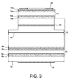
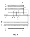
- Figures 3 and 4 are views schematic of the VCSEL structure, respectively before and after lateral oxidation.
- the same elements have the same references.
- GaAlAs layer with a high content of aluminum has the reference 22 in Figure 3 and the ring electrically insulating, in AlOx, has the reference 24 on Figure 4.
- the concentrated current lines are shown in Figure 4 and have the reference L2.
- the diameters obtained are usually in the following intervals: 5 to 10 ⁇ m for the unoxidized central window (the area let the current pass) and a few dozen micrometers for the total diameter of the insulating ring.
- the structure of the VCSEL is, indeed, completely reversible and just light it with a source centered on the emission wavelength of this VCSEL to make the latter a photo-detector very selective because only light centered on the peak resonance of the cavity that it contains may enter.
- the optical path in the cavity is not the even depending on whether the oxidized layer is crossed or not (the optical index of the latter being approximately 1,6), so the VCSEL detects at two lengths different waves, corresponding to the two thicknesses optical cavity (see documents [3] and [4]).
- this VCSEL will not be able to detect light from another VCSEL emitting at the same wavelength as him. he the first VCSEL will have to be associated with a second VCSEL emitting at a shorter wavelength. This second component will also not detect the light from the first because it will detect at a light of even shorter wavelength etc ..., hence a circle vicious.
- this VCSEL can not be used to detect the light returned by this object.
- the present invention aims to remedy the previous disadvantages. It aims in particular to solve the problem that follows.
- the first and second Rings are formed by partial oxidation of layers semiconductors that are parallel to the first and second mirrors and included in the cavity, the oxidation taking place in the whole portion of these layers that is located in the second part of the cavity and k being greater than n1 / (n1-n2), where n1 and n2 denote respectively the optical index of the material constituent of the semiconductor layers and the index optical of this material after oxidation.
- the cavity is made of a ternary semiconductor material A 1-x B x C, capable of being oxidized, with 0 ⁇ x ⁇ 1.
- Chemical elements A, B and C can be respectively Ga, Al and As.
- the active medium is a gain medium and the diode is a laser emitting the surface, with vertical cavity.
- the active medium is suitable for emit and detect the light and the diode is a light emitting diode with resonant cavity.
- the present invention also relates to a rangefinder comprising the diode according to the invention which constitutes a surface emission laser, vertical cavity.
- the invention further relates to a component light transceiver, comprising a matrix diodes according to the invention.
- the invention also relates to a rangefinder three-dimensional, comprising a matrix of diodes according to the invention, each of these diodes constituting a surface emission laser, vertical cavity.
- the solution of the problem posed above consists, for a VCSEL of the kind of FIG. 4, in adding one or more oxidizable layers to that which already exists (layer 24). These layers are redundant for the guide function of the current lines but make it possible to locally transform the cavity k x ⁇ into a cavity ( k -1) x ⁇ .
- N (AlAs), (N (AlOx) and N (GaAs) respectively denote the optical index of AlAs, the optical index of AlOx and the optical index of GaAs and D (AlAs) and D (GaAs) respectively designate the total thickness of AlAs and the total thickness of GaAs.
- Equation (1) describes the optical length of the cavity before oxidation and equation (2) describes the optical length of the same cavity after this oxidation.
- D (GaAs) 1 N (GaAs) x ( k - N (AlAs) NOT ( AlOx ) - N (AlOx) x ⁇ (5) with the important condition: k> N (AlAs) - N (AlOx) N (AlAs) and k natural whole (6)
- equation (3) can calculate the thickness of AlAs to be used (653.8nm) and one of two equations (1) and (2) gives the thickness of GaAs (186,8nm) which is necessary to complete the cavity.
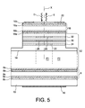
- Figure 5 illustrates the example that one just given about a diode consistent with the invention, operating at the same wavelength ⁇ for light emission E and light detection D.
- identical elements have the same references.
- the resonant cavity 12 of the VCSEL of Figure 5 contains two additional layers 26 and 28 that are identical to layer 22 and parallel to the latter (and therefore to the mirrors 8 and 16). These additional layers were inserted during the epitaxy leading to the stack that we see on Figure 5.
- the three layers were partially oxidized 24, 26 and 28 to get three parallel rings and electrically insulating 24, 20 and 32 in AlOx. These rings have the same inner diameter and the same outer diameter and have a common axis X which constitutes the VCSEL axis.
- the rings could be distributed on both sides of the quantum well layer 14 constituting the medium to gain.
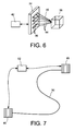
- Figure 6 schematically shows a example of a three-dimensional rangefinder, including a matrix 34 of VCSEL transceivers 36 conform to the invention.
- An object 38 for example a cube, receives a light pulse 40 sent by the first of VCSELs of the matrix, the latter being provided with electronic control and processing means 42.
- An optics not shown can also be placed between the matrix and the cube.
- the impulse is reflected by different points of the object and detected by others VCSELs from the matrix that are then used as than detectors.
- Electronic means 42 calculate the time differences between the different pulses reflected and detected 44. Then, the second VCSEL of the matrix emits a pulse and the other VCSELs detect the reflected pulse etc ....
- each VCSEL is used as a transmitter and receiver.
- the invention also applies to training bidirectional optical links. This is schematically illustrated by Figure 7 where we see two VCSEL transceivers 46 and 48 in accordance with the invention.
- VCSELs are connected by a fiber 50 and equipped with electronic means of order 52 which deals with the management of communications between VCSELs. These switch to turn of transmitter mode to receiver mode. In detecting the end of a message marked by a sequence well defined, the electronic means 52 use a mode of operation or the other.
- a sequence can be the following: send a signal by component 46, reception by the component 48, response by the component 48 which goes into transmission mode, reception by the component 46 that goes into receive mode.
- a RCLED according to the invention has the structure that we see in Figure 5 if only the Reflectivity of the mirrors is lower.
- a link can be formed bidirectional like that of Figure 7 in connecting two RCLEDs by an optical fiber.
Landscapes
- Physics & Mathematics (AREA)
- Optics & Photonics (AREA)
- Engineering & Computer Science (AREA)
- Condensed Matter Physics & Semiconductors (AREA)
- General Physics & Mathematics (AREA)
- Nanotechnology (AREA)
- Electromagnetism (AREA)
- Chemical & Material Sciences (AREA)
- Crystallography & Structural Chemistry (AREA)
- Biophysics (AREA)
- Life Sciences & Earth Sciences (AREA)
- Semiconductor Lasers (AREA)
- Luminescent Compositions (AREA)
- Led Device Packages (AREA)
- Optical Couplings Of Light Guides (AREA)
- Light Receiving Elements (AREA)
- Photo Coupler, Interrupter, Optical-To-Optical Conversion Devices (AREA)
Abstract
Description
- la télémétrie classique ou tridimensionnelle et
- les liens ou liaisons optiques pour les données ou les télécommunications mais également les liaisons entre cartes électroniques ou à l'intérieur d'un circuit électronique.
- des premier et deuxième miroirs,
- une cavité résonante délimitée par ces premier et deuxième miroirs,
- un milieu actif contenu dans cette cavité et apte à émettre et à détecter la lumière,
- un premier anneau électriquement isolant qui est parallèle aux premier et deuxième miroirs et placé dans la cavité d'un côté du milieu actif, ce premier anneau définissant deux parties dans la cavité, à savoir une première partie cylindrique qui traverse le premier anneau et une deuxième partie qui contient ce premier anneau,
- deux diodes émettrices-réceptrices conformes à l'invention, et
- un guide d'onde optique qui relie ces deux diodes.
- la figure 1 est une vue en perspective schématique de la structure d'un laser ruban classique et a déjà été décrite,
- la figure 2 est une vue en coupe schématique de la structure d'un VCSEL connu et a déjà été décrite,
- la figure 3 est une vue en coupe schématique d'un autre VCSEL connu, dont la cavité contient une couche destinée à être oxydée et a déjà été décrite,
- la figure 4 est une vue en coupe schématique de cet autre VCSEL après l'oxydation de cette couche et a déjà été décrite,
- la figure 5 est une vue en coupe schématique d'un VCSEL conforme à l'invention,
- la figure 6 illustre schématiquement l'application de la présente invention à la télémétrie tridimensionnelle, et
- la figure 7 illustre schématiquement l'application de la présente invention à la formation d'une liaison optique bidirectionnelle.
| GaAs | AlAs | |
| 3xλ | 186,8nm | 653,8nm |
| 4xλ | 429,7nm | 653,8nm |
| 5xλ | 672,5nm | 653,8nm |
Claims (10)
- Diode à cavité résonante, apte à émettre et à détecter une lumière de longueur d'onde λ, cette diode comprenant :cette diode étant caractérisée en ce qu'elle comprend en outre au moins un deuxième anneau électriquement isolant (30, 32) qui est parallèle aux premier et deuxième miroirs et placé dans la cavité d'un côté du milieu actif, ce deuxième anneau étant contenu dans la deuxième partie (P2) de la cavité et ayant le même diamètre intérieur et le même diamètre extérieur que le premier anneau, l'épaisseur totale des premier et deuxième anneaux étant prévue pour que la cavité résonante ait une longueur optique kxλ dans la première partie (P1) et une longueur optique (k-1)xλ dans la deuxième partie (P2), k étant un nombre entier au moins égal à 2.des premier et deuxième miroirs (8, 16),une cavité résonante (12) délimitée par ces premier et deuxième miroirs,un milieu actif (14) contenu dans cette cavité et apte à émettre et à détecter la lumière,un premier anneau électriquement isolant (24) qui est parallèle aux premier et deuxième miroirs et placé dans la cavité d'un côté du milieu actif, ce premier anneau définissant deux parties dans la cavité, à savoir une première partie cylindrique (P1) qui traverse le premier anneau et une deuxième partie (P2) qui contient ce premier anneau,
- Diode selon la revendication 1, dans laquelle les premier et deuxième anneaux (24, 30, 32) sont formés par oxydation partielle de couches semiconductrices (22, 26, 28) qui sont parallèles aux premier et deuxième miroirs et comprises dans la cavité, l'oxydation ayant lieu dans toute la portion de ces couches qui est située dans la deuxième partie (P2) de la cavité et k étant supérieur à n1/(n1-n2), où ni et n2 désignent respectivement l'indice optique du matériau constitutif des couches semiconductrices et l'indice optique de ce matériau après oxydation.
- Diode selon la revendication 2, dans laquelle la cavité (12) est faite d'un matériau semiconducteur ternaire A1-xBxC, apte à être oxydé, avec 0≤x≤1.
- Diode selon la revendication 3, dans laquelle les éléments chimiques A, B et C sont respectivement Ga, Al et As.
- Diode selon l'une quelconque des revendications 1 à 4, dans laquelle le milieu actif est un milieu à gain (14) et la diode est un laser à émission par la surface, à cavité verticale.
- Diode selon l'une quelconque des revendications 1 à 4, dans laquelle le milieu actif (54) est apte à émettre et à détecter la lumière et la diode est une diode électroluminescente à cavité résonante.
- Télémètre comprenant la diode selon la revendication 5.
- Composant émetteur-récepteur de lumière, comprenant une matrice (34) de diodes selon l'une quelconque des revendications 1 à 6.
- Télémètre à trois dimensions, comprenant une matrice (34) de diodes selon la revendication 5.
- Liaison optique bidirectionnelle comprenant :deux diodes émettrices-réceptrices (46, 48) selon l'une quelconque des revendications 1 à 6 etun guide d'onde optique (50) qui relie ces deux diodes.
Applications Claiming Priority (2)
| Application Number | Priority Date | Filing Date | Title |
|---|---|---|---|
| FR0350362A FR2858125B1 (fr) | 2003-07-23 | 2003-07-23 | Diode a cavite resonante, fonctionnant a la meme longueur d'onde pour l'emission et la detection de lumiere |
| FR0350362 | 2003-07-23 |
Publications (2)
| Publication Number | Publication Date |
|---|---|
| EP1501161A1 true EP1501161A1 (fr) | 2005-01-26 |
| EP1501161B1 EP1501161B1 (fr) | 2007-02-14 |
Family
ID=33484739
Family Applications (1)
| Application Number | Title | Priority Date | Filing Date |
|---|---|---|---|
| EP04103435A Expired - Lifetime EP1501161B1 (fr) | 2003-07-23 | 2004-07-19 | Diode à cavité résonante, fonctionnant à la même longueur d'onde pour l'émission et la détection de lumière |
Country Status (5)
| Country | Link |
|---|---|
| US (1) | US7170918B2 (fr) |
| EP (1) | EP1501161B1 (fr) |
| AT (1) | ATE354195T1 (fr) |
| DE (1) | DE602004004697T2 (fr) |
| FR (1) | FR2858125B1 (fr) |
Cited By (1)
| Publication number | Priority date | Publication date | Assignee | Title |
|---|---|---|---|---|
| DE102004057802A1 (de) * | 2004-11-30 | 2006-06-01 | Osram Opto Semiconductors Gmbh | Strahlungsemittierendes Halbleiterbauelement |
Families Citing this family (4)
| Publication number | Priority date | Publication date | Assignee | Title |
|---|---|---|---|---|
| TW201504599A (zh) * | 2013-05-30 | 2015-02-01 | Univ California | 具有高對比光柵及可作爲雙重用途之高對比光柵垂直腔表面發射雷射檢測器之二維週期結構的極化無關光檢測器 |
| EP3605605A1 (fr) * | 2018-08-01 | 2020-02-05 | MEAS France | Système émetteur-récepteur optique, barrière lumineuse et détecteur de pluie |
| US11016314B2 (en) * | 2018-08-14 | 2021-05-25 | International Business Machines Corporation | Non-volatilely programmable optical devices and methods to configure such optical devices |
| US10818807B2 (en) * | 2019-01-21 | 2020-10-27 | Globalfoundries Inc. | Semiconductor detectors integrated with Bragg reflectors |
Citations (6)
| Publication number | Priority date | Publication date | Assignee | Title |
|---|---|---|---|---|
| US4202000A (en) * | 1977-06-27 | 1980-05-06 | Thomson-Csf | Diode capable of alternately functioning as an emitter and detector of light of the same wavelength |
| US4948960A (en) * | 1988-09-20 | 1990-08-14 | The University Of Delaware | Dual mode light emitting diode/detector diode for optical fiber transmission lines |
| US5533041A (en) * | 1992-08-18 | 1996-07-02 | Fujitsu Limited | Optical transmission and reception device |
| US5978401A (en) * | 1995-10-25 | 1999-11-02 | Honeywell Inc. | Monolithic vertical cavity surface emitting laser and resonant cavity photodetector transceiver |
| EP1041690A1 (fr) * | 1999-03-29 | 2000-10-04 | Samsung Electronics Co., Ltd. | Module d'émission et de réception utilisant des lasers à émission par la surface |
| WO2001026102A1 (fr) * | 1999-10-05 | 2001-04-12 | New Dimension Research & Instrument, Inc. | Dispositif de servocommande et de captage optique monolithique vcsel |
-
2003
- 2003-07-23 FR FR0350362A patent/FR2858125B1/fr not_active Expired - Fee Related
-
2004
- 2004-07-19 DE DE602004004697T patent/DE602004004697T2/de not_active Expired - Fee Related
- 2004-07-19 EP EP04103435A patent/EP1501161B1/fr not_active Expired - Lifetime
- 2004-07-19 AT AT04103435T patent/ATE354195T1/de not_active IP Right Cessation
- 2004-07-22 US US10/895,851 patent/US7170918B2/en not_active Expired - Fee Related
Patent Citations (6)
| Publication number | Priority date | Publication date | Assignee | Title |
|---|---|---|---|---|
| US4202000A (en) * | 1977-06-27 | 1980-05-06 | Thomson-Csf | Diode capable of alternately functioning as an emitter and detector of light of the same wavelength |
| US4948960A (en) * | 1988-09-20 | 1990-08-14 | The University Of Delaware | Dual mode light emitting diode/detector diode for optical fiber transmission lines |
| US5533041A (en) * | 1992-08-18 | 1996-07-02 | Fujitsu Limited | Optical transmission and reception device |
| US5978401A (en) * | 1995-10-25 | 1999-11-02 | Honeywell Inc. | Monolithic vertical cavity surface emitting laser and resonant cavity photodetector transceiver |
| EP1041690A1 (fr) * | 1999-03-29 | 2000-10-04 | Samsung Electronics Co., Ltd. | Module d'émission et de réception utilisant des lasers à émission par la surface |
| WO2001026102A1 (fr) * | 1999-10-05 | 2001-04-12 | New Dimension Research & Instrument, Inc. | Dispositif de servocommande et de captage optique monolithique vcsel |
Non-Patent Citations (2)
| Title |
|---|
| STRITE S ET AL: "Tunable photodetectors and light-emitting diodes for wavelength division multiplexing", ELECTRONICS LETTERS, IEE STEVENAGE, GB, vol. 31, no. 8, 13 April 1995 (1995-04-13), pages 672 - 674, XP006002710, ISSN: 0013-5194 * |
| ZAKHAROV S M ET AL: "OPTOELECTRONIC INTEGRATED CIRCUITS UTILISING VERTICAL-CAVITY SURFACE-EMITTING SEMICONDUCTOR LASERS", QUANTUM ELECTRONICS, AMERICAN INSTITUTE OF PHYSICS, WOODBURY, NY, US, vol. 29, no. 9, September 1999 (1999-09-01), pages 745 - 761, XP000923961, ISSN: 1063-7818 * |
Cited By (3)
| Publication number | Priority date | Publication date | Assignee | Title |
|---|---|---|---|---|
| DE102004057802A1 (de) * | 2004-11-30 | 2006-06-01 | Osram Opto Semiconductors Gmbh | Strahlungsemittierendes Halbleiterbauelement |
| US7283577B2 (en) | 2004-11-30 | 2007-10-16 | Osram Opto Semiconductor Gmbh | Radiation-emitting semiconductor component |
| DE102004057802B4 (de) * | 2004-11-30 | 2011-03-24 | Osram Opto Semiconductors Gmbh | Strahlungemittierendes Halbleiterbauelement mit Zwischenschicht |
Also Published As
| Publication number | Publication date |
|---|---|
| US20050047465A1 (en) | 2005-03-03 |
| FR2858125A1 (fr) | 2005-01-28 |
| FR2858125B1 (fr) | 2005-08-26 |
| DE602004004697T2 (de) | 2007-10-31 |
| ATE354195T1 (de) | 2007-03-15 |
| DE602004004697D1 (de) | 2007-03-29 |
| EP1501161B1 (fr) | 2007-02-14 |
| US7170918B2 (en) | 2007-01-30 |
Similar Documents
| Publication | Publication Date | Title |
|---|---|---|
| JP4983346B2 (ja) | 半導体発光装置 | |
| US5732103A (en) | Long wavelength VCSEL | |
| US6674778B1 (en) | Electrically pumped edge-emitting photonic bandgap semiconductor laser | |
| US6148016A (en) | Integrated semiconductor lasers and photodetectors | |
| US6782027B2 (en) | Resonant reflector for use with optoelectronic devices | |
| JP2534444B2 (ja) | 集積化短キャビティ・レ―ザ | |
| FR3079080A1 (fr) | Vertical Cavity Surface Emitting Laser device with integrated tunnel junction | |
| US5883912A (en) | Long wavelength VCSEL | |
| US9716368B2 (en) | Tunable optical phase filter | |
| EP0545820A1 (fr) | Composant optique semi-conducteur à mode de sortie élargi et son procédé de fabrication | |
| FR3078835A1 (fr) | Dispositif photonique comportant un laser optiquement connecte a un guide d'onde silicium et procede de fabrication d'un tel dispositif photonique | |
| EP1285479B1 (fr) | Source a un photon a base d'emetteurs dont les frequences sont reparties de maniere choisie | |
| US20180048120A1 (en) | Semiconductor light emitting device | |
| EP1298461A1 (fr) | Réflecteur de Bragg distribué comprenant GaP et dispositif semi-conducteur à cavité résonante comprenant un tel RBD | |
| EP0091859B1 (fr) | Procédé de réalisation d'un laser à semi-conducteur à plusieurs longueurs d'onde indépendantes | |
| US20110103420A1 (en) | Laser diode | |
| JP2013122597A (ja) | 多重ファブリぺロー共振モードと多重吸収モードとを利用した透過型イメージ変調器および透過型イメージ変調器を形成する方法 | |
| EP1501161B1 (fr) | Diode à cavité résonante, fonctionnant à la même longueur d'onde pour l'émission et la détection de lumière | |
| JP2005158922A (ja) | 表面発光型半導体レーザ素子およびその製造方法 | |
| EP1257027A1 (fr) | Dispositif optique comportant une pluralité de cavités résonantes de longuers différentes associées à différentes longuers d'ondes | |
| JP4650631B2 (ja) | 半導体発光装置 | |
| US6208680B1 (en) | Optical devices having ZNS/CA-MG-fluoride multi-layered mirrors | |
| EP4369537A2 (fr) | Laser à émission par la surface à cavité verticale à émission par le bas à jonctions multiples et son procédé de fabrication | |
| CN220253752U (zh) | 垂直腔面发射激光器 | |
| US20030227952A1 (en) | VCSEL device with single-mode output |
Legal Events
| Date | Code | Title | Description |
|---|---|---|---|
| PUAI | Public reference made under article 153(3) epc to a published international application that has entered the european phase |
Free format text: ORIGINAL CODE: 0009012 |
|
| AK | Designated contracting states |
Kind code of ref document: A1 Designated state(s): AT BE BG CH CY CZ DE DK EE ES FI FR GB GR HU IE IT LI LU MC NL PL PT RO SE SI SK TR |
|
| AX | Request for extension of the european patent |
Extension state: AL HR LT LV MK |
|
| 17P | Request for examination filed |
Effective date: 20050715 |
|
| AKX | Designation fees paid |
Designated state(s): AT BE BG CH CY CZ DE DK EE ES FI FR GB GR HU IE IT LI LU MC NL PL PT RO SE SI SK TR |
|
| GRAP | Despatch of communication of intention to grant a patent |
Free format text: ORIGINAL CODE: EPIDOSNIGR1 |
|
| RIN1 | Information on inventor provided before grant (corrected) |
Inventor name: GROSSE, PHILIPPE |
|
| RTI1 | Title (correction) |
Free format text: RESONANT CAVITY DIODE, OPERATING AT THE SAME WAVELENGTH FOR EMISSION AND DETECTION OF LIGHT |
|
| RAP1 | Party data changed (applicant data changed or rights of an application transferred) |
Owner name: COMMISSARIAT A L'ENERGIE ATOMIQUE |
|
| GRAS | Grant fee paid |
Free format text: ORIGINAL CODE: EPIDOSNIGR3 |
|
| GRAA | (expected) grant |
Free format text: ORIGINAL CODE: 0009210 |
|
| AK | Designated contracting states |
Kind code of ref document: B1 Designated state(s): AT BE BG CH CY CZ DE DK EE ES FI FR GB GR HU IE IT LI LU MC NL PL PT RO SE SI SK TR |
|
| PG25 | Lapsed in a contracting state [announced via postgrant information from national office to epo] |
Ref country code: DK Free format text: LAPSE BECAUSE OF FAILURE TO SUBMIT A TRANSLATION OF THE DESCRIPTION OR TO PAY THE FEE WITHIN THE PRESCRIBED TIME-LIMIT Effective date: 20070214 Ref country code: NL Free format text: LAPSE BECAUSE OF FAILURE TO SUBMIT A TRANSLATION OF THE DESCRIPTION OR TO PAY THE FEE WITHIN THE PRESCRIBED TIME-LIMIT Effective date: 20070214 Ref country code: PL Free format text: LAPSE BECAUSE OF FAILURE TO SUBMIT A TRANSLATION OF THE DESCRIPTION OR TO PAY THE FEE WITHIN THE PRESCRIBED TIME-LIMIT Effective date: 20070214 Ref country code: AT Free format text: LAPSE BECAUSE OF FAILURE TO SUBMIT A TRANSLATION OF THE DESCRIPTION OR TO PAY THE FEE WITHIN THE PRESCRIBED TIME-LIMIT Effective date: 20070214 Ref country code: IE Free format text: LAPSE BECAUSE OF FAILURE TO SUBMIT A TRANSLATION OF THE DESCRIPTION OR TO PAY THE FEE WITHIN THE PRESCRIBED TIME-LIMIT Effective date: 20070214 Ref country code: SI Free format text: LAPSE BECAUSE OF FAILURE TO SUBMIT A TRANSLATION OF THE DESCRIPTION OR TO PAY THE FEE WITHIN THE PRESCRIBED TIME-LIMIT Effective date: 20070214 Ref country code: FI Free format text: LAPSE BECAUSE OF FAILURE TO SUBMIT A TRANSLATION OF THE DESCRIPTION OR TO PAY THE FEE WITHIN THE PRESCRIBED TIME-LIMIT Effective date: 20070214 |
|
| REG | Reference to a national code |
Ref country code: GB Ref legal event code: FG4D Free format text: NOT ENGLISH |
|
| REG | Reference to a national code |
Ref country code: CH Ref legal event code: EP |
|
| REF | Corresponds to: |
Ref document number: 602004004697 Country of ref document: DE Date of ref document: 20070329 Kind code of ref document: P |
|
| REG | Reference to a national code |
Ref country code: IE Ref legal event code: FG4D Free format text: LANGUAGE OF EP DOCUMENT: FRENCH |
|
| PG25 | Lapsed in a contracting state [announced via postgrant information from national office to epo] |
Ref country code: SE Free format text: LAPSE BECAUSE OF FAILURE TO SUBMIT A TRANSLATION OF THE DESCRIPTION OR TO PAY THE FEE WITHIN THE PRESCRIBED TIME-LIMIT Effective date: 20070514 |
|
| PG25 | Lapsed in a contracting state [announced via postgrant information from national office to epo] |
Ref country code: BG Free format text: LAPSE BECAUSE OF FAILURE TO SUBMIT A TRANSLATION OF THE DESCRIPTION OR TO PAY THE FEE WITHIN THE PRESCRIBED TIME-LIMIT Effective date: 20070515 |
|
| GBT | Gb: translation of ep patent filed (gb section 77(6)(a)/1977) |
Effective date: 20070425 |
|
| PG25 | Lapsed in a contracting state [announced via postgrant information from national office to epo] |
Ref country code: ES Free format text: LAPSE BECAUSE OF FAILURE TO SUBMIT A TRANSLATION OF THE DESCRIPTION OR TO PAY THE FEE WITHIN THE PRESCRIBED TIME-LIMIT Effective date: 20070525 |
|
| PG25 | Lapsed in a contracting state [announced via postgrant information from national office to epo] |
Ref country code: PT Free format text: LAPSE BECAUSE OF FAILURE TO SUBMIT A TRANSLATION OF THE DESCRIPTION OR TO PAY THE FEE WITHIN THE PRESCRIBED TIME-LIMIT Effective date: 20070716 |
|
| NLV1 | Nl: lapsed or annulled due to failure to fulfill the requirements of art. 29p and 29m of the patents act | ||
| REG | Reference to a national code |
Ref country code: IE Ref legal event code: FD4D |
|
| PG25 | Lapsed in a contracting state [announced via postgrant information from national office to epo] |
Ref country code: SK Free format text: LAPSE BECAUSE OF FAILURE TO SUBMIT A TRANSLATION OF THE DESCRIPTION OR TO PAY THE FEE WITHIN THE PRESCRIBED TIME-LIMIT Effective date: 20070214 |
|
| PLBE | No opposition filed within time limit |
Free format text: ORIGINAL CODE: 0009261 |
|
| STAA | Information on the status of an ep patent application or granted ep patent |
Free format text: STATUS: NO OPPOSITION FILED WITHIN TIME LIMIT |
|
| PG25 | Lapsed in a contracting state [announced via postgrant information from national office to epo] |
Ref country code: CZ Free format text: LAPSE BECAUSE OF FAILURE TO SUBMIT A TRANSLATION OF THE DESCRIPTION OR TO PAY THE FEE WITHIN THE PRESCRIBED TIME-LIMIT Effective date: 20070214 Ref country code: RO Free format text: LAPSE BECAUSE OF FAILURE TO SUBMIT A TRANSLATION OF THE DESCRIPTION OR TO PAY THE FEE WITHIN THE PRESCRIBED TIME-LIMIT Effective date: 20070214 |
|
| 26N | No opposition filed |
Effective date: 20071115 |
|
| BERE | Be: lapsed |
Owner name: COMMISSARIAT A L'ENERGIE ATOMIQUE Effective date: 20070731 |
|
| PG25 | Lapsed in a contracting state [announced via postgrant information from national office to epo] |
Ref country code: MC Free format text: LAPSE BECAUSE OF NON-PAYMENT OF DUE FEES Effective date: 20070731 Ref country code: GR Free format text: LAPSE BECAUSE OF FAILURE TO SUBMIT A TRANSLATION OF THE DESCRIPTION OR TO PAY THE FEE WITHIN THE PRESCRIBED TIME-LIMIT Effective date: 20070515 |
|
| REG | Reference to a national code |
Ref country code: FR Ref legal event code: ST Effective date: 20080331 |
|
| PG25 | Lapsed in a contracting state [announced via postgrant information from national office to epo] |
Ref country code: BE Free format text: LAPSE BECAUSE OF NON-PAYMENT OF DUE FEES Effective date: 20070731 |
|
| PG25 | Lapsed in a contracting state [announced via postgrant information from national office to epo] |
Ref country code: FR Free format text: LAPSE BECAUSE OF NON-PAYMENT OF DUE FEES Effective date: 20070731 |
|
| PG25 | Lapsed in a contracting state [announced via postgrant information from national office to epo] |
Ref country code: EE Free format text: LAPSE BECAUSE OF FAILURE TO SUBMIT A TRANSLATION OF THE DESCRIPTION OR TO PAY THE FEE WITHIN THE PRESCRIBED TIME-LIMIT Effective date: 20070214 |
|
| REG | Reference to a national code |
Ref country code: CH Ref legal event code: PL |
|
| PG25 | Lapsed in a contracting state [announced via postgrant information from national office to epo] |
Ref country code: CH Free format text: LAPSE BECAUSE OF NON-PAYMENT OF DUE FEES Effective date: 20080731 Ref country code: LI Free format text: LAPSE BECAUSE OF NON-PAYMENT OF DUE FEES Effective date: 20080731 |
|
| PG25 | Lapsed in a contracting state [announced via postgrant information from national office to epo] |
Ref country code: CY Free format text: LAPSE BECAUSE OF FAILURE TO SUBMIT A TRANSLATION OF THE DESCRIPTION OR TO PAY THE FEE WITHIN THE PRESCRIBED TIME-LIMIT Effective date: 20070214 |
|
| PG25 | Lapsed in a contracting state [announced via postgrant information from national office to epo] |
Ref country code: LU Free format text: LAPSE BECAUSE OF NON-PAYMENT OF DUE FEES Effective date: 20070719 |
|
| PG25 | Lapsed in a contracting state [announced via postgrant information from national office to epo] |
Ref country code: HU Free format text: LAPSE BECAUSE OF FAILURE TO SUBMIT A TRANSLATION OF THE DESCRIPTION OR TO PAY THE FEE WITHIN THE PRESCRIBED TIME-LIMIT Effective date: 20070815 Ref country code: TR Free format text: LAPSE BECAUSE OF FAILURE TO SUBMIT A TRANSLATION OF THE DESCRIPTION OR TO PAY THE FEE WITHIN THE PRESCRIBED TIME-LIMIT Effective date: 20070214 |
|
| PGFP | Annual fee paid to national office [announced via postgrant information from national office to epo] |
Ref country code: DE Payment date: 20090722 Year of fee payment: 6 Ref country code: GB Payment date: 20090720 Year of fee payment: 6 |
|
| PGFP | Annual fee paid to national office [announced via postgrant information from national office to epo] |
Ref country code: IT Payment date: 20090725 Year of fee payment: 6 |
|
| GBPC | Gb: european patent ceased through non-payment of renewal fee |
Effective date: 20100719 |
|
| PG25 | Lapsed in a contracting state [announced via postgrant information from national office to epo] |
Ref country code: DE Free format text: LAPSE BECAUSE OF NON-PAYMENT OF DUE FEES Effective date: 20110201 |
|
| REG | Reference to a national code |
Ref country code: DE Ref legal event code: R119 Ref document number: 602004004697 Country of ref document: DE Effective date: 20110201 |
|
| PG25 | Lapsed in a contracting state [announced via postgrant information from national office to epo] |
Ref country code: IT Free format text: LAPSE BECAUSE OF NON-PAYMENT OF DUE FEES Effective date: 20100719 |
|
| PG25 | Lapsed in a contracting state [announced via postgrant information from national office to epo] |
Ref country code: GB Free format text: LAPSE BECAUSE OF NON-PAYMENT OF DUE FEES Effective date: 20100719 |