EP1501152A1 - Millimeter-wave signal transition device - Google Patents
Millimeter-wave signal transition device Download PDFInfo
- Publication number
- EP1501152A1 EP1501152A1 EP04254416A EP04254416A EP1501152A1 EP 1501152 A1 EP1501152 A1 EP 1501152A1 EP 04254416 A EP04254416 A EP 04254416A EP 04254416 A EP04254416 A EP 04254416A EP 1501152 A1 EP1501152 A1 EP 1501152A1
- Authority
- EP
- European Patent Office
- Prior art keywords
- waveguide
- transition
- mode
- signal
- transducer
- Prior art date
- Legal status (The legal status is an assumption and is not a legal conclusion. Google has not performed a legal analysis and makes no representation as to the accuracy of the status listed.)
- Granted
Links
Images


Classifications
-
- H—ELECTRICITY
- H01—ELECTRIC ELEMENTS
- H01P—WAVEGUIDES; RESONATORS, LINES, OR OTHER DEVICES OF THE WAVEGUIDE TYPE
- H01P5/00—Coupling devices of the waveguide type
- H01P5/08—Coupling devices of the waveguide type for linking dissimilar lines or devices
- H01P5/10—Coupling devices of the waveguide type for linking dissimilar lines or devices for coupling balanced lines or devices with unbalanced lines or devices
- H01P5/107—Hollow-waveguide/strip-line transitions
Definitions
- This invention relates generally to a millimeter-wave signal transition, and, more specifically, to a signal transition for transiting a mm-wave signal between two different geometric planes.
- ACC Automated cruise control
- ACC allows a user to set the desired speed and minimum following distance of his/her vehicle.
- the system then controls the speed of the user's vehicle to ensure that the minimum following distance is maintained.
- Critical to such systems is the effective implementation of a radar system, typically those operating in the 77 GHz range.
- Such systems must be capable of transmitting, receiving and manipulating millimeter-wave (mm-wave) signals.
- mm-wave millimeter-wave
- a signal transition in an electrical circuit is to transfer the radio frequency (RF) energy from one point to another point with minimum interference and loss.
- RF radio frequency
- the key requirements of a good signal transition are high return loss and low insertion loss. Note that, in general, these two specifications are independent from each other, but must be satisfied simultaneously. In other words, one may achieve a relatively good return loss using a particular signal transition, however, without having a low insertion loss, mm-wave energy is absorbed in the transition, thereby diminishing the total performance of the system. Having a low insertion loss is especially important in high frequencies due to increased conductor and radiation losses.
- Transitions designed to transfer electrical signals from a transverse plane of microstrip lines to another plane, which is parallel to the first one, with a vertical connection are now going to be explained in more detail because the invention is related with such structures. Via holes employed in standard multi-layer printed circuit board (PCB) technology are very good examples of such transitions.
- PCB printed circuit board
- the critical issue here is the electrical length of the vertical connection. As the length of vertical connection increases, design of the transition becomes more challenging because of the increased parasitic inductance.
- the microstrip-to-slot transition along with its variants which use a vertical waveguide section is one of the more commonly used techniques for this purpose. This approach, however, has a number of disadvantages.
- this transition relies on the resonance phenomenon to achieve a good match. Therefore it is particularly susceptible to geometry variations in the transition. Additionally, since the transition has no back short, it suffers from relatively high insertion loss due to radiation. This is especially important because the spurious radiations that may occur in such a transition may increase the cross talk or affect the antenna pattern in a mm-wave system.
- a transition can be used which exploits an E-plane probe with a back short to transfer the energy through a waveguide section.
- This approached is well established in the literature, it has a significant disadvantage in mm-wave frequencies. Specifically, at these frequencies, one must position a back short over a microstrip probe within a tolerance in the order of sub-millimeters in a 77 GHz application. This is clearly an expensive procedure for a high volume manufacturing.
- the present invention fulfills this need among others.
- the present invention provides a mm-wave signal transition which overcomes the problems of the prior art. Specifically, the transition of the present invention uses a transducer to convert signals between transverse electromagnetic (TEM) and waveguide modes, rather than relying on the precise positioning of a transmission line relative to a waveguide to launch a signal down the waveguide.
- TEM transverse electromagnetic
- the sensitive signal conversion between TEM mode and waveguide mode is performed in a single, modular unit, which lends itself to mass manufacturing using well-known techniques.
- the converted signal can be transmitted to an orthogonally positioned transmission line or waveguide with relative ease. If desired, the signal can then be converted back to either a TEM mode or waveguide mode signal for transmission down a different orthogonally positioned transmission line or waveguide. This allows the signal to be transmitted over various types of transmission lines over relatively large distances between circuits with efficiency.
- the TEM/waveguide mode conversion is performed in a transducer, which can be manufactured discretely using well-known techniques, the need for close tolerance positioning between the other components of the transition is alleviated, thereby facilitating large-scale manufacturing techniques and modularization.
- the waveguide need not be precisely aligned with the transition line, but may instead be based on a relatively loosely toleranced borehole through a support plate. This borehole may be adapted to receive a separately manufactured, modular waveguide filler to aid in the propagation of the waveguide mode signal.
- the transducer not only simplifies the assembly of the transition, but also, in its preferred embodiment, it is planar and eliminates the need for back short, thereby simplifying its own manufacture. Therefore, the present invention's exploitation of a transducer in a transition offers significant manufacturing benefits over the prior art.
- one aspect of the present invention is a transition for transmitting a mm-wave from one plane to another plane using a transducer.
- the transition comprises: (a) first and second transmission lines on parallel planes; (b) a third transmission line orthogonal to the first and second transmission lines, wherein either the first and second transmission lines are suitable for transmitting a TEM mode signal and the third transmission line is suitable for transmitting a hollow waveguide mode signal, or the third transmission line is suitable for transmitting a TEM mode signal and the first and second transmission lines are suitable for transmitting a waveguide mode signal; and (c) first and second transducers, the first transducer coupled between the first and third transmission lines, the second transducer coupled between the second and third transmission lines, each of the transducers being suitable for converting a signal between TEM and hollow waveguide modes.
- Another aspect of the present invention is a method for transmitting a mm-wave signal from a first plane to a second plane using a transition comprising a transducer.
- the method comprises: (a) transmitting a mm-wave signal along a first transmission line in a first plane; (b) converting the signal from one mode of either a TEM mode or a waveguide mode to the other mode of either the TEM mode or the waveguide mode using a transducer; (c) transmitting the signal along a third transmission line orthogonal to the first transmission line in the other mode to a second plane parallel to the first plane; (d) converting the signal back to the one mode; and (e) transmitting the signal in the one mode along a second transmission line in the second plane.
- the method comprises: (a) providing a support plate; (b) boring a hole in the support plate to form the waveguide; (c) inserting a waveguide filler in the hole; (d) providing first and second mm-wave boards, each board comprising an integrated transmission line and a transducer having a waveguide portion; (e) affixing the first and second mm-wave boards to each side of the support plate such that the transition lines are orthogonal to the waveguide and that the waveguide is axially aligned with the waveguide portion of each transducer.
- Yet another aspect of the invention is a system incorporating the transition of the present invention.
- the system comprises an ACC system with the transition described above.
- the term “transition” refers to any device either integral, integrally-molded or an assembly of discrete components which is used to transmit a mm-wave signal from one transverse plane to another one.
- the term “mm-wave signal” refers to a high-frequency electrical signal which may be propagating in a number of different forms, including, for example, in a transverse electromagnetic (TEM) mode or in a waveguide mode.
- TEM mode refers collectively to both a true TEM pattern and a quasi-TEM pattern. The concepts of TEM, quasi-TEM, and hollow waveguide fields are well known and will not be addressed specifically herein.
- the term "hollow waveguide mode” as used herein refers to a mode in which electromagnetic energy propagates in a waveguide.
- the term hollow is employed to indicate that the waveguide does not have a center conductor as in coaxial waveguides. However, it may have a dielectric filling to alter the propagation properties. Therefore, this type of waveguide cannot support TEM mode propagation.
- Hollow waveguide modes are well known and depend on the type of waveguide through which the signal is intended to travel. For example, a fundamental mode for a rectangular waveguide is the TE 10 mode, while the fundamental mode for a circular waveguide is a TE 01 mode.
- Transition 1 comprises first and second parallel transmission lines 2a, 2b, and a third transmission line 4 orthogonal to the first and second transmission lines 2a, 2b.
- the first and second transmission lines are incorporated into first and second mm-wave boards 6, 7, which are on different transverse planes.
- the first and second transmission lines 2a, 2b are suitable for transmitting a signal having a TEM mode
- the third transmission line 4 is a waveguide 4a disposed in a support plate 5 and is suitable for transmitting a signal in a waveguide mode.
- the transition 1 also comprises first and second transducers 3a, 3b on the first and second mm-wave boards 6,7, respectively.
- the first transducer 3a is coupled between the first and third transmission lines 2a, 4, while the second transducer 3b is coupled between the second and third transmission lines 2b, 4.
- Each of the transducers converts a signal between a TEM mode and a waveguide mode.
- the first and second transmission lines 2a, 2b of the present invention are suitable for transmitting TEM mode signals to and from the first and second transducers 3a, 3b, respectively, while the third transmission line 4 is a waveguide 4a suitable for transmitting a waveguide mode signal between the transducers. It is within the scope of the invention, however, that functionality of the transmission lines be reversed and that the first and second transmission lines are instead waveguides, while the third transmission line is a general transmission line suitable for supporting a TEM mode signal between the two transducers. The particular configuration of the transmission lines depends upon the desired application.
- the former is generally preferred in assemblies used in ACC systems due to the anticipated incorporation of the first and second transmission lines into other circuitry used for the generation, receipt and manipulation/interpretation of the signal because microstrip lines (i.e., quasi-TEM waveguide) are used to carry RF signals in such systems.
- microstrip lines i.e., quasi-TEM waveguide
- this discussion will focus on the embodiment in which mm-wave signals are transmitted between parallel transmission lines using a waveguide.
- Transmission lines for transmitting TEM and waveguide mode signals are well known.
- Examples of transmission lines for transmitting TEM signals include coaxial lines, striplines, microstrip lines, coplanar waveguides (CPW), and fin strips.
- at least one of the transmission lines suitable for transmitting TEM signals is a coplanar transmission line, specifically, a microstrip. More preferably, both the first and second transmission lines are microstrips.
- the first mm-wave board 6 is shown comprising the first transition line 2a and the first transducer 3a.
- the second mm-wave board 7, which comprises the second transmission line 2b and second transducer 3b is identical to the first mm-wave board such that one mm-board configuration may be used for both planes.
- the first transmission line 2a is embodied as a microstrip 21.
- the configuration of a microstrip is well known and comprises a conductive path 21 printed onto the first substrate 26.
- the conductive path 21 connects or couples external circuitry to the transition 1.
- the short length of conductive path 21, therefore, may be an extension of a transmission line carrying a communications signal to or from the external circuitry on the mm-wave board or a separate circuit board.
- the microstrip may comprise any known conductor such as copper, gold, silver or aluminum.
- the dimensions of the microstrip can vary depending upon the application and the material used.
- the width of the microstrip line depends on the characteristic impedance required. For example, on a 5 mils thick Duroid 5880 material, which has the dielectric constant of 2.2, the 50-Ohm microstrip transmission line is 15 mils wide.
- the substrate 26 may be any structure that provides a platform for supporting the conductive path 21.
- the substrate is also suitable for supporting other electrical and optical components such as the transducer.
- the conductive path 21 and other components may be mounted in or on the substrate or may be integrally formed or integrated with the substrate.
- the substrate 26 is rigid to provide a stable platform for the electrical components affixed thereto, although flexible substrates are contemplated herein as well.
- the substrate is preferably, although not necessarily, planar.
- the substrate is often an integral component of a transmission line or transducer, and, thus, its electrical properties may be critical.
- Suitable materials for the substrate include dielectrics having a dielectric constant between about 2 and 10.
- suitable materials include ceramics such as Alumina, single crystal semiconductors such as Gallium Arsenide and Silicon, single crystal sapphire, glass, quartz, and plastics such as Teflon®. Satisfactory results have been obtained with a substrate of Duroid® 5880 (a Teflon based material, commercially-available through Rogers Corporation) which has an effective dielectric constant of 2.2.
- the substrate should be adequately dimensioned to provide a sufficient base for the first conductive path 21, and, preferably, the first transducer 3a, although it should be understood that the transducer and transmission lines may be supported by discrete substrates and coupled via an additional transition suitable for coupling TEM mode signals between different transmission lines on the same plane (well known).
- One of ordinary skill in the art can determine the appropriate thickness for a particular substrate material.
- the third transmission line 4 is a waveguide 4a for transmitting the signal in a waveguide mode.
- Waveguides are well known and include hollow, solid and filled waveguides of all shapes and cross-sectional areas and lengths.
- the waveguide is a filled rectangular waveguide given its relative ease of manufacturing.
- Those of ordinary skill in the art will appreciate, however, that although a rectangular waveguide is described herein, the invention also applies to waveguides with cross-sectional geometries that are not rectilinear, such as, for example, circular cross sections.
- the waveguide is a hollow rectangular waveguide defined by a tunnel or bore hole through the support plate 5.
- the support plate 5 may be desirable to add rigidity of the assembly and make it more robust.
- the support plate 5 comprises a relatively thick, rigid material, such as a metal plate 5a, for supporting the first and second mm-wave boards 6, 7.
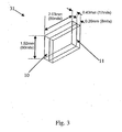
- the borehole is filled with a separately prepared dielectric substrate filling 31 with rectangular cross-section as shown in Fig. 3.
- This dielectric substrate filling 31 has a thick metal backing 10 and a dielectric material 11.
- the dielectric material used in the filling 31 can be selected from a wide range of materials. Suitable materials tend to have a dielectric constant of about 2.2 to about 12.9, and a loss tangent of about 0.001 to about 0.01. Examples of suitable materials include ceramic, Teflon, GaAs, and Silicon, which are the commonly used mm-wave board materials or substrates for monolithic microwave circuits. For example, suitable results have been achieved using Alumina which has a dielectric constant of 9.6 and a loss tangent of 0.001.
- the backside metalization of the boards should be relatively thick.
- suitable results have been achieved using 0.43mm (17 mils) of aluminum material and 0,20mm (8 mils) of Alumina.
- the important point is to select proper dielectric thickness to match the characteristic impedance of the waveguide portion of transducer 4 (discussed below). This can be easily achieved using a full-wave electromagnetic simulator.
- the dielectric and the backside metallization of the filling material After determining the thickness of the dielectric and the backside metallization of the filling material through the design process, they are cut in the shape of rectangular prisms to form the completed dielectric substrate filling 31 and dropped into the rectangular opening previously prepared in the metal plate 5a. This way, a rectangular dielectric-filled waveguide 4 is formed in the metal plate 5a, which is used to transfer the mm-wave energy from one side of the metal plate 5a to the other side.
- the length of waveguide 4 may be as thick as the support plate 5 or the vertical distance between the first and second transmission lines 2a, 2b. This means that the waveguide may have a length which is greater than 10% of the wavelength of the mm-wave signal. For example, if the wavelength is 2.8 mm (77GHz), the length may be greater than 0.28 mm. Such lengths have proven problematic in the prior art, however, since the present invention employs a filled waveguide section to transfer the mm-wave energy, it is possible to transfer the energy through thicker support plates with relatively low loss. In a preferred embodiment, the length of waveguide section is at least 0.25 mm, more preferably, at least 1 mm, and, even more preferably, at least 1.5 mm.
- the first and second transducers 3a, 3b serves to convert the signal between the TEM mode and waveguide mode.
- the concept of using a transducer is discussed generally in U.S. Patent No. 6,087,907 which is hereby incorporated by reference.
- the first transducer 3a is considered in detail with respect to the first mm-wave board 6, although it should be appreciated that the second transducer 3b is preferably identical to the first transducer, and thus, the discussion herein applies to the second transducer as well.
- the first transducer 3a may be separated into three different portions: the transmission portion 23, the conversion portion 24 and the waveguide portion 25.
- the transmission portion 23 of the transducer 3a is electrically coupled to the conductive path 21 of the first transmission line 2a.
- the transducer and transmission line may be printed on the same substrate as the transmission line and consequently a clear line of demarcation between the two may not exist. Nevertheless, for purposes of discussion herein suffice it to say that, at some point 22 (perhaps hypothetical), the conductive path 21 is no longer part of the transmission line 2a but rather part of the transmission portion 23 of the transducer 3 a.
- the transmission portion 23 is connected to the conversion portion 24.
- the conversion portion 24 comprises a plurality of conductive converting fins 28 printed onto the first substrate 26.
- the use of fins minimizes the reflective loss of the transducer.
- Each fin 28 is disposed in perpendicular relation to the direction of TEM mode propagation. In the embodiment shown in Fig. 2, each fin 28 is positioned co-linear with its pair fin and on opposite sides of a conversion trace 27 which is axially aligned with the TEM axis. In this embodiment, there are four pairs of converting fins 28. Each fin 28 is equal to or greater than one-quarter wavelength of the operating frequency in length where the length of the fin is defined from the TEM axis to the end of each fin.
- the central operating frequency is 77 GHz.
- One quarter of a wavelength of microstrip in Duroid® substrate having a dielectric constant of 2.2 at a central operating frequency of 77 GHz is, therefore, approximately 1.02mm (40 mils).
- a width of the conversion portion 24 using fins 28 on opposite sides of the conversion trace 27 is approximately equal to or greater than 2.04mm (80 mils) total.
- Alternative embodiments also include fewer pairs of fins 28 as well as additional pairs of fins 28 or transmission lines comprising the conversion portion 24 depending upon the desired electrical performance.
- the fins 28 electrically behave as transmission lines.
- the appropriate length of the transmission line electrically creates what appears to be an open circuit near, but away from the center of the TEM axis by virtue of the approximately one-quarter wavelength dimension.
- the transmission line may also be emulated using a lumped element equivalent circuit instead of the fin 28, for example a parallel inductor and capacitor combination having appropriate values at the operating frequency.
- the conversion portion is adjacent the waveguide portion 25 of the transducer 3a.
- the waveguide portion 25 comprises the first substrate 26 and a U-shaped conductive barrier 29 defining a portion of the first waveguide's perimeter.
- the barrier 29 may be formed in known ways including etching or machining a trench or series of recessions in the substrate and filling or lining the trench or recessions with a conductive material such as, for example, gold, silver, copper, or aluminum. Rather than forming a continuous trench in the substrate, it may be preferable to use closely spaced circular vias to approximate a trench wall. Such an approach may be preferred for a printed circuit board. However, a continuous trench would improve the isolation between the neighbouring transitions significantly.
- a waveguide mode signal is launched into the waveguide portion by the conversion portion. Specifically, since adjacent fins 28 are electrically close together, the currents flowing through the fins are approximately in phase. The currents through the fins induce magnetic and electric fields that interfere destructively in air, but interfere constructively in the dielectric. Most of the energy, therefore, is transferred into the first substrate 26 of the waveguide portion 25.
- the specific configuration of the transducer and the waveguide may be determined using commercially available full-wave electromagnetic simulators.
- the design process may employ a simulation and optimization of appropriately portioned structures using a full-wave 3D electromagnetic simulator, available though, for example, Ansoft HFSS.
- the optimization feature of the simulator allows one to vary the dimensions of the transition for different material properties, sizes, and operating frequencies.
- the TEM mode signal is carried by the first transmission line 2a to the transmission portion 23 of the first transducer 3a.
- the signal is converted to a waveguide mode, in particular, a TE 10 mode, for launching into a rectangular waveguide portion 25 of the first transducer 3a formed in the first substrate 26.
- the signal propagating through the waveguide portion 25 of the first transducer 3a is transferred to the third transmission line 4, the waveguide 4a, via a waveguide junction.
- the mm-wave signal passes through the waveguide 4a, it is coupled to a waveguide portion (not shown) of the second transducer 3b on a second substrate and is converted back to a TEM mode signal and transmitted to the transmission portion (not shown) of the second transducer 3b.
- the TEM mode signal is finally coupled to the second transmission line 2b which is parallel to the first transmission line 2a. This completes the transfer of the mm-wave signal from the first transmission line 2a to the second transmission line 2b.
- the transducer may work in reverse as well. Specifically, in the preferred embodiment, the same transducer can be used to convert a waveguide mode signal inputted into its waveguide portion to a TEM mode signal which is outputted through its transition portion.
- the configuration of the transition of the present invention provides for improved manufacturability.
- the design avoids the close tolerances required in prior art transitions such as, for example, microstrip-to-slot and E-plane probe transitions.
- the conversion is effected in a modular component and complex alignment between components and waveguides can be avoided. Consequently, production methods can be used which lend themselves to volume and automated assembly.
- the waveguide can be made separately from the transition-that is, it does not need to be formed integrally with the transition. This allows it to be manufactured using high-volume manufacturing techniques. For example, in the embodiment shown in Fig.
- the waveguide in formed in the support plate 5, the metal base plate 5a by first boring an opening in the substrate corresponding to the cross-section area of the waveguide.
- the waveguide is rectangular and, hence, the opening is rectangular.
- the dimensions of this rectangular section are larger than the required dimensions for the waveguide section of the transition.
- the actual waveguide function is formed by a separately prepared metalized dielectric which is dropped into this opening. The reason for initially preparing a larger opening in the base is to facilitate high-volume manufacturing requirements because it would be extremely difficult to machine the actual waveguide dimensions directly into the metal plate due to low tolerance requirements.
- the transition of the present invention not only lends itself to high-volume manufacturing techniques, but also offers improved performance.
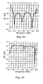
- Fig. 4 the simulated response of the mm-wave transition of Fig. 1 is shown. Note that the reflection loss of the transition is better than 15 dB between 65 and 85 GHz. The insertion loss is better than 0.6 dB in the same frequency range.
- the transition of the present invention may be utilized in any assembly in which a mm-wave signal is transferred from one plane to another plane.
- Examples of such assemblies include ACC systems, LMDS systems and HRR systems.
Landscapes
- Waveguides (AREA)
- Waveguide Aerials (AREA)
- Radar Systems Or Details Thereof (AREA)
Abstract
Description
- This invention relates generally to a millimeter-wave signal transition, and, more specifically, to a signal transition for transiting a mm-wave signal between two different geometric planes.
- Automated cruise control (ACC) for automobiles is gaining popularity in recent years. ACC allows a user to set the desired speed and minimum following distance of his/her vehicle. The system then controls the speed of the user's vehicle to ensure that the minimum following distance is maintained. Critical to such systems is the effective implementation of a radar system, typically those operating in the 77 GHz range. Such systems must be capable of transmitting, receiving and manipulating millimeter-wave (mm-wave) signals. As with most electronics, there is continuous pressure to miniaturize such systems to reduce their space and material requirements. Consequently, the circuitry of these systems is becoming more compact and sophisticated, employing such techniques as stack circuit technology to reduce size. With stacked circuits, there is often a need to transmit a signal between circuit substrates while operating in the mm-wave domain. For example, in ACC system applications, transreceiver and antenna are placed on either sides of a thick support plate. This makes it necessary to transmit the mm-wave signal between two microstrips on either side of the relatively thick metal support plate. This transmission is performed by a "signal transition" or "transition" as used herein. Design of this transition is critical to the overall system performance.
- The purpose of a signal transition in an electrical circuit is to transfer the radio frequency (RF) energy from one point to another point with minimum interference and loss. The key requirements of a good signal transition are high return loss and low insertion loss. Note that, in general, these two specifications are independent from each other, but must be satisfied simultaneously. In other words, one may achieve a relatively good return loss using a particular signal transition, however, without having a low insertion loss, mm-wave energy is absorbed in the transition, thereby diminishing the total performance of the system. Having a low insertion loss is especially important in high frequencies due to increased conductor and radiation losses.
- Transitions designed to transfer electrical signals from a transverse plane of microstrip lines to another plane, which is parallel to the first one, with a vertical connection are now going to be explained in more detail because the invention is related with such structures. Via holes employed in standard multi-layer printed circuit board (PCB) technology are very good examples of such transitions. The critical issue here is the electrical length of the vertical connection. As the length of vertical connection increases, design of the transition becomes more challenging because of the increased parasitic inductance. There are a number of reported developments for transferring a signal from one transverse plane to another one. For example, the microstrip-to-slot transition along with its variants which use a vertical waveguide section is one of the more commonly used techniques for this purpose. This approach, however, has a number of disadvantages. First, this transition relies on the resonance phenomenon to achieve a good match. Therefore it is particularly susceptible to geometry variations in the transition. Additionally, since the transition has no back short, it suffers from relatively high insertion loss due to radiation. This is especially important because the spurious radiations that may occur in such a transition may increase the cross talk or affect the antenna pattern in a mm-wave system. Alternatively, a transition can be used which exploits an E-plane probe with a back short to transfer the energy through a waveguide section. Although this approached is well established in the literature, it has a significant disadvantage in mm-wave frequencies. Specifically, at these frequencies, one must position a back short over a microstrip probe within a tolerance in the order of sub-millimeters in a 77 GHz application. This is clearly an expensive procedure for a high volume manufacturing.
- Therefore, there is a need for a mm-wave transition to overcome the aforementioned difficulties. The present invention fulfills this need among others.
- The present invention provides a mm-wave signal transition which overcomes the problems of the prior art. Specifically, the transition of the present invention uses a transducer to convert signals between transverse electromagnetic (TEM) and waveguide modes, rather than relying on the precise positioning of a transmission line relative to a waveguide to launch a signal down the waveguide. By using a transducer, the sensitive signal conversion between TEM mode and waveguide mode is performed in a single, modular unit, which lends itself to mass manufacturing using well-known techniques. Once the delicate operation of converting a signal between TEM and waveguide modes is performed, the converted signal can be transmitted to an orthogonally positioned transmission line or waveguide with relative ease. If desired, the signal can then be converted back to either a TEM mode or waveguide mode signal for transmission down a different orthogonally positioned transmission line or waveguide. This allows the signal to be transmitted over various types of transmission lines over relatively large distances between circuits with efficiency.
- This approach offers a number of advantages over prior art approaches with respect to both manufacturing and performance. As mentioned above, since the TEM/waveguide mode conversion is performed in a transducer, which can be manufactured discretely using well-known techniques, the need for close tolerance positioning between the other components of the transition is alleviated, thereby facilitating large-scale manufacturing techniques and modularization. For example, the waveguide need not be precisely aligned with the transition line, but may instead be based on a relatively loosely toleranced borehole through a support plate. This borehole may be adapted to receive a separately manufactured, modular waveguide filler to aid in the propagation of the waveguide mode signal. Additionally, by converting the TEM/waveguide mode in a modular transducer, there is no need to interconnect probes or the like through soldering or other welding techniques which are time-consuming and prone to failure or performance variations. The transducer not only simplifies the assembly of the transition, but also, in its preferred embodiment, it is planar and eliminates the need for back short, thereby simplifying its own manufacture. Therefore, the present invention's exploitation of a transducer in a transition offers significant manufacturing benefits over the prior art.
- In addition to the manufacturing benefits of the present invention, it also offers important performance advantages over the prior art. Specifically, by converting between TEM and waveguide modes in a relatively simple, modular unit, a complex assembly of components is eliminated along with its attendant inefficiencies and variances. This results in a transition that provides consistent performance with both low insert loss and low reflective loss. Additionally, since the signal transition between orthogonal transmission lines is performed by converting the mode of the signal, the distance over which signals may be communicatively connected to parallel transmission lines is limited by the loss of the vertical hollow-waveguide which can be relatively low. This is in stark contrast to many prior art devices which experience difficulty in transmitting mm-wave signals between parallel transmissions that are further than 10% of the operating signal's wavelength. Finally, since the transition does not use probes or similar antenna like devices to launch the signal into the waveguide, radiation losses are very low and there is no need for a back short.
- Accordingly, one aspect of the present invention is a transition for transmitting a mm-wave from one plane to another plane using a transducer. In a preferred embodiment, the transition comprises: (a) first and second transmission lines on parallel planes; (b) a third transmission line orthogonal to the first and second transmission lines, wherein either the first and second transmission lines are suitable for transmitting a TEM mode signal and the third transmission line is suitable for transmitting a hollow waveguide mode signal, or the third transmission line is suitable for transmitting a TEM mode signal and the first and second transmission lines are suitable for transmitting a waveguide mode signal; and (c) first and second transducers, the first transducer coupled between the first and third transmission lines, the second transducer coupled between the second and third transmission lines, each of the transducers being suitable for converting a signal between TEM and hollow waveguide modes.
- Another aspect of the present invention is a method for transmitting a mm-wave signal from a first plane to a second plane using a transition comprising a transducer. In a preferred embodiment, the method comprises: (a) transmitting a mm-wave signal along a first transmission line in a first plane; (b) converting the signal from one mode of either a TEM mode or a waveguide mode to the other mode of either the TEM mode or the waveguide mode using a transducer; (c) transmitting the signal along a third transmission line orthogonal to the first transmission line in the other mode to a second plane parallel to the first plane; (d) converting the signal back to the one mode; and (e) transmitting the signal in the one mode along a second transmission line in the second plane.
- Another aspect of the present invention is a method of manufacturing a transition which lends itself to large-scale manufacturing. In a preferred embodiment, the method comprises: (a) providing a support plate; (b) boring a hole in the support plate to form the waveguide; (c) inserting a waveguide filler in the hole; (d) providing first and second mm-wave boards, each board comprising an integrated transmission line and a transducer having a waveguide portion; (e) affixing the first and second mm-wave boards to each side of the support plate such that the transition lines are orthogonal to the waveguide and that the waveguide is axially aligned with the waveguide portion of each transducer.
- Yet another aspect of the invention is a system incorporating the transition of the present invention. In a preferred embodiment, the system comprises an ACC system with the transition described above.
- An embodiment of the present invention will now be described by way of example with reference to the accompanying drawings, in which:
- Fig. 1 shows a preferred embodiment of the transition of the present invention.
- Fig. 2 shows the substrate of the transition of Fig. 1.
- Fig. 3 shows the waveguide filler for the transition of Fig. 1.
- Fig. 4a and 4b show performance data for the transition of Fig. 1.
-
- Referring to Fig. 1, a preferred embodiment of the
signal transition 1 of the present invention is shown. As used herein, the term "transition" refers to any device either integral, integrally-molded or an assembly of discrete components which is used to transmit a mm-wave signal from one transverse plane to another one. As used herein, the term "mm-wave signal" refers to a high-frequency electrical signal which may be propagating in a number of different forms, including, for example, in a transverse electromagnetic (TEM) mode or in a waveguide mode. As used herein, the term "TEM mode" refers collectively to both a true TEM pattern and a quasi-TEM pattern. The concepts of TEM, quasi-TEM, and hollow waveguide fields are well known and will not be addressed specifically herein. Suffice it to say though, that in a true TEM mode the electrical field, the magnetic field and the direction of wave travel are all orthogonal to each other, while in a quasi-TEM mode, the electrical field, the magnetic field and the direction of wave travel are generally orthogonal to each other although there are small longitudinal electric and magnetic fields components. The term "hollow waveguide mode" as used herein refers to a mode in which electromagnetic energy propagates in a waveguide. The term hollow is employed to indicate that the waveguide does not have a center conductor as in coaxial waveguides. However, it may have a dielectric filling to alter the propagation properties. Therefore, this type of waveguide cannot support TEM mode propagation. Hollow waveguide modes are well known and depend on the type of waveguide through which the signal is intended to travel. For example, a fundamental mode for a rectangular waveguide is the TE10 mode, while the fundamental mode for a circular waveguide is a TE01 mode. -
Transition 1 comprises first and secondparallel transmission lines second transmission lines wave boards second transmission lines transition 1 also comprises first andsecond transducers wave boards first transducer 3a is coupled between the first andthird transmission lines 2a, 4, while thesecond transducer 3b is coupled between the second andthird transmission lines 2b, 4. Each of the transducers converts a signal between a TEM mode and a waveguide mode. These components are considered below in greater detail. - In the embodiment of Fig. 1, the first and
second transmission lines second transducers - Transmission lines for transmitting TEM and waveguide mode signals are well known. Examples of transmission lines for transmitting TEM signals include coaxial lines, striplines, microstrip lines, coplanar waveguides (CPW), and fin strips. Preferably, at least one of the transmission lines suitable for transmitting TEM signals is a coplanar transmission line, specifically, a microstrip. More preferably, both the first and second transmission lines are microstrips.
- Referring to Fig. 2, the first mm-
wave board 6 is shown comprising thefirst transition line 2a and thefirst transducer 3a. Preferably, but not necessarily, the second mm-wave board 7, which comprises thesecond transmission line 2b andsecond transducer 3b, is identical to the first mm-wave board such that one mm-board configuration may be used for both planes. Thefirst transmission line 2a is embodied as amicrostrip 21. As mentioned above, the configuration of a microstrip is well known and comprises aconductive path 21 printed onto thefirst substrate 26. When incorporated in an ACC system or other mm-wave based system, theconductive path 21 connects or couples external circuitry to thetransition 1. The short length ofconductive path 21, therefore, may be an extension of a transmission line carrying a communications signal to or from the external circuitry on the mm-wave board or a separate circuit board. - The microstrip may comprise any known conductor such as copper, gold, silver or aluminum. The dimensions of the microstrip can vary depending upon the application and the material used. The width of the microstrip line depends on the characteristic impedance required. For example, on a 5 mils thick Duroid 5880 material, which has the dielectric constant of 2.2, the 50-Ohm microstrip transmission line is 15 mils wide.
- The
substrate 26 may be any structure that provides a platform for supporting theconductive path 21. Preferably, the substrate is also suitable for supporting other electrical and optical components such as the transducer. Theconductive path 21 and other components may be mounted in or on the substrate or may be integrally formed or integrated with the substrate. As a matter of convention, when referring to a component's position with respect to a substrate, the terms "on," "in," "incorporated into," and "integrally-formed" are used interchangeably throughout this disclosure. Preferably, thesubstrate 26 is rigid to provide a stable platform for the electrical components affixed thereto, although flexible substrates are contemplated herein as well. Additionally, the substrate is preferably, although not necessarily, planar. - Aside from its physical configuration, the substrate is often an integral component of a transmission line or transducer, and, thus, its electrical properties may be critical. Suitable materials for the substrate include dielectrics having a dielectric constant between about 2 and 10. Examples of suitable materials include ceramics such as Alumina, single crystal semiconductors such as Gallium Arsenide and Silicon, single crystal sapphire, glass, quartz, and plastics such as Teflon®. Satisfactory results have been obtained with a substrate of Duroid® 5880 (a Teflon based material, commercially-available through Rogers Corporation) which has an effective dielectric constant of 2.2.
- The substrate should be adequately dimensioned to provide a sufficient base for the first
conductive path 21, and, preferably, thefirst transducer 3a, although it should be understood that the transducer and transmission lines may be supported by discrete substrates and coupled via an additional transition suitable for coupling TEM mode signals between different transmission lines on the same plane (well known). One of ordinary skill in the art can determine the appropriate thickness for a particular substrate material. - In the embodiment shown in Fig. 1, the third transmission line 4 is a waveguide 4a for transmitting the signal in a waveguide mode. Waveguides are well known and include hollow, solid and filled waveguides of all shapes and cross-sectional areas and lengths. Preferably, the waveguide is a filled rectangular waveguide given its relative ease of manufacturing. Those of ordinary skill in the art will appreciate, however, that although a rectangular waveguide is described herein, the invention also applies to waveguides with cross-sectional geometries that are not rectilinear, such as, for example, circular cross sections.
- Referring to Fig. 1, the waveguide is a hollow rectangular waveguide defined by a tunnel or bore hole through the support plate 5. In addition to defining the waveguide, the support plate 5 may be desirable to add rigidity of the assembly and make it more robust. For example, in the embodiment shown in Fig. 1, the support plate 5 comprises a relatively thick, rigid material, such as a metal plate 5a, for supporting the first and second mm-
wave boards - In the embodiment shown in Fig. 1, the borehole is filled with a separately prepared dielectric substrate filling 31 with rectangular cross-section as shown in Fig. 3. This dielectric substrate filling 31 has a
thick metal backing 10 and adielectric material 11. The dielectric material used in the filling 31 can be selected from a wide range of materials. Suitable materials tend to have a dielectric constant of about 2.2 to about 12.9, and a loss tangent of about 0.001 to about 0.01. Examples of suitable materials include ceramic, Teflon, GaAs, and Silicon, which are the commonly used mm-wave board materials or substrates for monolithic microwave circuits. For example, suitable results have been achieved using Alumina which has a dielectric constant of 9.6 and a loss tangent of 0.001. For this application, the backside metalization of the boards should be relatively thick. For example, suitable results have been achieved using 0.43mm (17 mils) of aluminum material and 0,20mm (8 mils) of Alumina. The important point is to select proper dielectric thickness to match the characteristic impedance of the waveguide portion of transducer 4 (discussed below). This can be easily achieved using a full-wave electromagnetic simulator. - After determining the thickness of the dielectric and the backside metallization of the filling material through the design process, they are cut in the shape of rectangular prisms to form the completed dielectric substrate filling 31 and dropped into the rectangular opening previously prepared in the metal plate 5a. This way, a rectangular dielectric-filled waveguide 4 is formed in the metal plate 5a, which is used to transfer the mm-wave energy from one side of the metal plate 5a to the other side.
- The length of waveguide 4 may be as thick as the support plate 5 or the vertical distance between the first and
second transmission lines - The first and
second transducers first transducer 3a is considered in detail with respect to the first mm-wave board 6, although it should be appreciated that thesecond transducer 3b is preferably identical to the first transducer, and thus, the discussion herein applies to the second transducer as well. - For illustrative purposes, the
first transducer 3a may be separated into three different portions: thetransmission portion 23, theconversion portion 24 and thewaveguide portion 25. Thetransmission portion 23 of thetransducer 3a is electrically coupled to theconductive path 21 of thefirst transmission line 2a. It should be understood that the transducer and transmission line may be printed on the same substrate as the transmission line and consequently a clear line of demarcation between the two may not exist. Nevertheless, for purposes of discussion herein suffice it to say that, at some point 22 (perhaps hypothetical), theconductive path 21 is no longer part of thetransmission line 2a but rather part of thetransmission portion 23 of thetransducer 3 a. - The
transmission portion 23 is connected to theconversion portion 24. Theconversion portion 24 comprises a plurality of conductive converting fins 28 printed onto thefirst substrate 26. The use of fins minimizes the reflective loss of the transducer. Each fin 28 is disposed in perpendicular relation to the direction of TEM mode propagation. In the embodiment shown in Fig. 2, each fin 28 is positioned co-linear with its pair fin and on opposite sides of aconversion trace 27 which is axially aligned with the TEM axis. In this embodiment, there are four pairs of converting fins 28. Each fin 28 is equal to or greater than one-quarter wavelength of the operating frequency in length where the length of the fin is defined from the TEM axis to the end of each fin. For example, in the present embodiment, the central operating frequency is 77 GHz. One quarter of a wavelength of microstrip in Duroid® substrate having a dielectric constant of 2.2 at a central operating frequency of 77 GHz is, therefore, approximately 1.02mm (40 mils). Accordingly, a width of theconversion portion 24 using fins 28 on opposite sides of theconversion trace 27 is approximately equal to or greater than 2.04mm (80 mils) total. Alternative embodiments also include fewer pairs of fins 28 as well as additional pairs of fins 28 or transmission lines comprising theconversion portion 24 depending upon the desired electrical performance. - In operation, it can be thought that the fins 28 electrically behave as transmission lines. At the operating frequency, the appropriate length of the transmission line electrically creates what appears to be an open circuit near, but away from the center of the TEM axis by virtue of the approximately one-quarter wavelength dimension. The transmission line, however, may also be emulated using a lumped element equivalent circuit instead of the fin 28, for example a parallel inductor and capacitor combination having appropriate values at the operating frequency. In alternate embodiments, it is not necessary that the fins 28 in each pair be co-linear with each other or that there be an equal number of fins 28 on either side of the
conversion trace 27. Modifying these characteristics, however, will vary performance characteristics. These characteristics, therefore, may be used to optimize performance of the transformer for specific applications. - The conversion portion is adjacent the
waveguide portion 25 of thetransducer 3a. Thewaveguide portion 25 comprises thefirst substrate 26 and a U-shapedconductive barrier 29 defining a portion of the first waveguide's perimeter. Thebarrier 29 may be formed in known ways including etching or machining a trench or series of recessions in the substrate and filling or lining the trench or recessions with a conductive material such as, for example, gold, silver, copper, or aluminum. Rather than forming a continuous trench in the substrate, it may be preferable to use closely spaced circular vias to approximate a trench wall. Such an approach may be preferred for a printed circuit board. However, a continuous trench would improve the isolation between the neighbouring transitions significantly. - A waveguide mode signal is launched into the waveguide portion by the conversion portion. Specifically, since adjacent fins 28 are electrically close together, the currents flowing through the fins are approximately in phase. The currents through the fins induce magnetic and electric fields that interfere destructively in air, but interfere constructively in the dielectric. Most of the energy, therefore, is transferred into the
first substrate 26 of thewaveguide portion 25. - The specific configuration of the transducer and the waveguide may be determined using commercially available full-wave electromagnetic simulators. For example, the design process may employ a simulation and optimization of appropriately portioned structures using a full-wave 3D electromagnetic simulator, available though, for example, Ansoft HFSS. The optimization feature of the simulator allows one to vary the dimensions of the transition for different material properties, sizes, and operating frequencies.
- Referring to Figs. 1 and 2, the operation of the
transition 1 is now considered. The TEM mode signal is carried by thefirst transmission line 2a to thetransmission portion 23 of thefirst transducer 3a. In the transducer, the signal is converted to a waveguide mode, in particular, a TE10 mode, for launching into arectangular waveguide portion 25 of thefirst transducer 3a formed in thefirst substrate 26. Then, the signal propagating through thewaveguide portion 25 of thefirst transducer 3a is transferred to the third transmission line 4, the waveguide 4a, via a waveguide junction. After the mm-wave signal passes through the waveguide 4a, it is coupled to a waveguide portion (not shown) of thesecond transducer 3b on a second substrate and is converted back to a TEM mode signal and transmitted to the transmission portion (not shown) of thesecond transducer 3b. The TEM mode signal is finally coupled to thesecond transmission line 2b which is parallel to thefirst transmission line 2a. This completes the transfer of the mm-wave signal from thefirst transmission line 2a to thesecond transmission line 2b. - It should be understood that although the function of the transducer was described above with respect to the transducer converting a TEM mode signal inputted into its transmission portion to a waveguide mode signal which is outputted through its waveguide portion, the transducer may work in reverse as well. Specifically, in the preferred embodiment, the same transducer can be used to convert a waveguide mode signal inputted into its waveguide portion to a TEM mode signal which is outputted through its transition portion.
- As mentioned above, the configuration of the transition of the present invention provides for improved manufacturability. Specifically, the design avoids the close tolerances required in prior art transitions such as, for example, microstrip-to-slot and E-plane probe transitions. By relying on a transducer to convert the signal between TEM and waveguide modes, the conversion is effected in a modular component and complex alignment between components and waveguides can be avoided. Consequently, production methods can be used which lend themselves to volume and automated assembly. In particular, since the transmission line to waveguide position is not critical, the waveguide can be made separately from the transition-that is, it does not need to be formed integrally with the transition. This allows it to be manufactured using high-volume manufacturing techniques. For example, in the embodiment shown in Fig. 1, the waveguide in formed in the support plate 5, the metal base plate 5a, by first boring an opening in the substrate corresponding to the cross-section area of the waveguide. In the preferred embodiment, the waveguide is rectangular and, hence, the opening is rectangular. The dimensions of this rectangular section are larger than the required dimensions for the waveguide section of the transition. However, the actual waveguide function is formed by a separately prepared metalized dielectric which is dropped into this opening. The reason for initially preparing a larger opening in the base is to facilitate high-volume manufacturing requirements because it would be extremely difficult to machine the actual waveguide dimensions directly into the metal plate due to low tolerance requirements.
- The transition of the present invention not only lends itself to high-volume manufacturing techniques, but also offers improved performance. For example, referring to Fig. 4, the simulated response of the mm-wave transition of Fig. 1 is shown. Note that the reflection loss of the transition is better than 15 dB between 65 and 85 GHz. The insertion loss is better than 0.6 dB in the same frequency range.
- The transition of the present invention may be utilized in any assembly in which a mm-wave signal is transferred from one plane to another plane. Examples of such assemblies include ACC systems, LMDS systems and HRR systems.
Claims (33)
- A transition (1) for transmitting a mm-wave signal from one plane to another,
said transition comprising:first and second transmission lines (2a,2b) on parallel planes;
a third transmission line (4) orthogonal to said first and second transmission lines (2a,2b), wherein either said first and second transmission lines (2a,2b) are suitable for transmitting a TEM or transverse electromagnetic mode signal and said third transmission line (4) is suitable for transmitting a waveguide mode signal, or said third transmission line (4) is suitable for transmitting a TEM mode signal and said first and second transmission lines (2a,2b) are suitable for transmitting a waveguide mode signal; andfirst and second transducers (3a,3b), said first transducer (3a) coupled between said first and third transmission lines (2a,4), said second transducer (3b) coupled between said second and third transmission lines (2b,4), each of said transducers (3a,3b) being suitable for converting a signal between TEM and waveguide modes. - The transition (1) of claim 1, wherein said third transmission line (4) is a waveguide (4a).
- The transition (1) of claim 2, wherein said first or second transmission line (2a,2b) is a microstrip (21).
- The transition (1) of claim 1, 2 or 3, wherein said first and second transmission lines (2a,2b) and said first and second transducers (3a,3b) are disposed on first and second mm-wave boards (6,7), respectively.
- The transition (1) of claim 4, wherein said mm-wave boards (6,7) are overlapping.
- The transition (1) of claim 4 or 5, wherein said mm-wave boards (6,7) are separated by a distance of at least 10% of an operating signal wavelength.
- The transition (1) of claim 4, 5 or 6, wherein at least one of said mm-wave boards (6,7) comprises electrical circuitry.
- The transition (1) of any preceding claim, wherein said first transducer (3a) converts a signal from a TEM mode to a waveguide mode and said second transducer (3b) converts a signal from a waveguide mode to a TEM mode.
- The transition (1) of claim 8, wherein said waveguide mode is a rectangular waveguide mode.
- The transition (1) of claim 8 or 9, wherein said rectangular waveguide mode is a TE10 mode.
- The transition (1) of any preceding claim, wherein each transducer (3a,3b) comprises:a transmission portion (23) connected to the respective transmission line (2a,2b) of the transducer (3a,3b);a waveguide portion (25) configured to facilitate the propagation of a waveguide mode signal therethrough in a plane orthogonal to the transmission portion; anda conversion portion (24) electrically connected between said transmission portion (23) and said waveguide portion (25), said conversion portion (24) being configured to convert a signal between a TEM mode and a waveguide mode.
- The transition (1) of claim 11, wherein said conversion portion (24) comprises at least one fin (28) perpendicular to the direction of propagation of the TEM mode signal.
- The transition (1) of claim 11 or 12, wherein said transmission portion (23), said waveguide portion (25), and said conversion portion (24) share a common substrate (26).
- The transition (1) of claim 13, wherein said waveguide portion (25) comprises a conductive barrier defined in said substrate (26).
- The transition (1) of claim 14, wherein said conductive barrier is a metallic wall.
- The transition (1) of claim 14, wherein said conductive barrier is a perforated metallic wall.
- The transition of any preceding claim, wherein said first and second transducers (3a,3b) are identical.
- The transition (1) of claim 2, or any claim depending thereon, wherein said waveguide (4a) is a hollow waveguide.
- The transition (1) of claim 2, or any claim depending thereon, wherein said waveguide (4a) is a rectangular waveguide.
- The transition (1) of claim 2, or any claim depending thereon, wherein said waveguide (4a) has a length of at least 0.25 mm.
- The transition (1) of claim 2, or any claim depending thereon, wherein said waveguide (4a) comprises a metalized dielectric filler (10,11).
- The transition (1) of claims 2 and 11, wherein said waveguide (4a) comprises a metalized dielectric filler (10,11) having an impedance which matches that of said waveguide portion (25).
- The transition (1) of claim 2, or any claim depending thereon, further comprising a support plate (5) between said first and second transmission lines (2a,2b) and through which said waveguide passes.
- The transition (1) of claim 23, wherein said support plate (5) is rigid.
- The transition (1) of claim 23 or 24, wherein said support plate (5) is metal.
- The transition (1) of claim 23, 24 or 25, wherein said support plate (5) comprises a borehole (31) to accommodate said waveguide (4a).
- The transition (1) of any one of claims 23 to 26, wherein said support plate (5) is at least 1mm thick.
- An ACC or automatic cruise control system comprising the transition (1) of any preceding claim.
- A method for transmitting a mm-wave signal from a first plane to a second plane using a transition (1), the method comprising:transmitting a mm-wave signal along a first transmission line (2a) in a first plane;converting said signal from one mode of either a TEM or transverse electromagnetic mode or a waveguide mode to the other mode of either said TEM mode or said waveguide mode using a transducer (3a);transmitting said signal along a third transmission line (4) orthogonal to said first transmission line (2a) in said other mode to a second plane parallel to said first plane;converting said signal back to said one mode; andtransmitting said signal in said one mode along a second transmission line (2b) in said second plane.
- The method of claim 29, wherein said signal is between about 65 to about 85 GHz.
- The method of claim 29 or 30, wherein resulting reflective loss is better than 15 dB and resulting insertion loss is better than 0.6 dB.
- The method of claim 29, 30 or 31, wherein a dimension of said third transmission line (4) is greater than 10% of the wavelength of said signal.
- A method of manufacturing a transition (1), said method comprising:providing a support plate (5);boring a hole in said support plate (5);inserting a waveguide (4a) in said hole (5);providing first and second mm-wave boards (6,7), each mm-wave board (6,7) comprising an integrated transmission line (2a,2b) and a transducer (3a,3b) having a waveguide portion (25); andaffixing said first and second mm-wave boards (6,7) to each side of said support plate (5) such that said transmission lines (2a,2b) are orthogonal to said waveguide (4a) and such that said waveguide (4a) is axially aligned with said waveguide portion (25) of each transducer (3a,3b).
Applications Claiming Priority (2)
| Application Number | Priority Date | Filing Date | Title |
|---|---|---|---|
| US628635 | 2003-07-25 | ||
| US10/628,635 US6952143B2 (en) | 2003-07-25 | 2003-07-25 | Millimeter-wave signal transmission device |
Publications (2)
| Publication Number | Publication Date |
|---|---|
| EP1501152A1 true EP1501152A1 (en) | 2005-01-26 |
| EP1501152B1 EP1501152B1 (en) | 2010-08-11 |
Family
ID=33490928
Family Applications (1)
| Application Number | Title | Priority Date | Filing Date |
|---|---|---|---|
| EP04254416A Expired - Lifetime EP1501152B1 (en) | 2003-07-25 | 2004-07-23 | Millimeter-wave signal transition device |
Country Status (5)
| Country | Link |
|---|---|
| US (1) | US6952143B2 (en) |
| EP (1) | EP1501152B1 (en) |
| JP (1) | JP2005045815A (en) |
| CN (1) | CN1619331A (en) |
| DE (1) | DE602004028554D1 (en) |
Cited By (2)
| Publication number | Priority date | Publication date | Assignee | Title |
|---|---|---|---|---|
| EP3203257A4 (en) * | 2014-10-03 | 2018-06-13 | Universitat Politécnica de Valencia | Device for calibrating network analysers |
| CN116895929A (en) * | 2023-08-03 | 2023-10-17 | 上海英恒电子有限公司 | A transmission line transition structure and radar system circuit stacked architecture |
Families Citing this family (140)
| Publication number | Priority date | Publication date | Assignee | Title |
|---|---|---|---|---|
| JP4365852B2 (en) * | 2006-11-30 | 2009-11-18 | 株式会社日立製作所 | Waveguide structure |
| JP4648292B2 (en) * | 2006-11-30 | 2011-03-09 | 日立オートモティブシステムズ株式会社 | Millimeter-wave transceiver and in-vehicle radar using the same |
| JP5374994B2 (en) * | 2008-09-25 | 2013-12-25 | ソニー株式会社 | Millimeter-wave dielectric transmission device |
| US9999038B2 (en) | 2013-05-31 | 2018-06-12 | At&T Intellectual Property I, L.P. | Remote distributed antenna system |
| US9525524B2 (en) | 2013-05-31 | 2016-12-20 | At&T Intellectual Property I, L.P. | Remote distributed antenna system |
| US8897697B1 (en) | 2013-11-06 | 2014-11-25 | At&T Intellectual Property I, Lp | Millimeter-wave surface-wave communications |
| US9768833B2 (en) | 2014-09-15 | 2017-09-19 | At&T Intellectual Property I, L.P. | Method and apparatus for sensing a condition in a transmission medium of electromagnetic waves |
| US10063280B2 (en) | 2014-09-17 | 2018-08-28 | At&T Intellectual Property I, L.P. | Monitoring and mitigating conditions in a communication network |
| US9615269B2 (en) | 2014-10-02 | 2017-04-04 | At&T Intellectual Property I, L.P. | Method and apparatus that provides fault tolerance in a communication network |
| US9685992B2 (en) | 2014-10-03 | 2017-06-20 | At&T Intellectual Property I, L.P. | Circuit panel network and methods thereof |
| US9503189B2 (en) | 2014-10-10 | 2016-11-22 | At&T Intellectual Property I, L.P. | Method and apparatus for arranging communication sessions in a communication system |
| US9973299B2 (en) | 2014-10-14 | 2018-05-15 | At&T Intellectual Property I, L.P. | Method and apparatus for adjusting a mode of communication in a communication network |
| US9762289B2 (en) | 2014-10-14 | 2017-09-12 | At&T Intellectual Property I, L.P. | Method and apparatus for transmitting or receiving signals in a transportation system |
| US9627768B2 (en) | 2014-10-21 | 2017-04-18 | At&T Intellectual Property I, L.P. | Guided-wave transmission device with non-fundamental mode propagation and methods for use therewith |
| US9780834B2 (en) | 2014-10-21 | 2017-10-03 | At&T Intellectual Property I, L.P. | Method and apparatus for transmitting electromagnetic waves |
| US9312919B1 (en) | 2014-10-21 | 2016-04-12 | At&T Intellectual Property I, Lp | Transmission device with impairment compensation and methods for use therewith |
| US9769020B2 (en) | 2014-10-21 | 2017-09-19 | At&T Intellectual Property I, L.P. | Method and apparatus for responding to events affecting communications in a communication network |
| US9653770B2 (en) | 2014-10-21 | 2017-05-16 | At&T Intellectual Property I, L.P. | Guided wave coupler, coupling module and methods for use therewith |
| US9577306B2 (en) | 2014-10-21 | 2017-02-21 | At&T Intellectual Property I, L.P. | Guided-wave transmission device and methods for use therewith |
| US9544006B2 (en) | 2014-11-20 | 2017-01-10 | At&T Intellectual Property I, L.P. | Transmission device with mode division multiplexing and methods for use therewith |
| US9742462B2 (en) | 2014-12-04 | 2017-08-22 | At&T Intellectual Property I, L.P. | Transmission medium and communication interfaces and methods for use therewith |
| US9997819B2 (en) | 2015-06-09 | 2018-06-12 | At&T Intellectual Property I, L.P. | Transmission medium and method for facilitating propagation of electromagnetic waves via a core |
| US10340573B2 (en) | 2016-10-26 | 2019-07-02 | At&T Intellectual Property I, L.P. | Launcher with cylindrical coupling device and methods for use therewith |
| US9800327B2 (en) | 2014-11-20 | 2017-10-24 | At&T Intellectual Property I, L.P. | Apparatus for controlling operations of a communication device and methods thereof |
| US9461706B1 (en) | 2015-07-31 | 2016-10-04 | At&T Intellectual Property I, Lp | Method and apparatus for exchanging communication signals |
| US10243784B2 (en) | 2014-11-20 | 2019-03-26 | At&T Intellectual Property I, L.P. | System for generating topology information and methods thereof |
| US10009067B2 (en) | 2014-12-04 | 2018-06-26 | At&T Intellectual Property I, L.P. | Method and apparatus for configuring a communication interface |
| US9954287B2 (en) | 2014-11-20 | 2018-04-24 | At&T Intellectual Property I, L.P. | Apparatus for converting wireless signals and electromagnetic waves and methods thereof |
| US9876570B2 (en) | 2015-02-20 | 2018-01-23 | At&T Intellectual Property I, Lp | Guided-wave transmission device with non-fundamental mode propagation and methods for use therewith |
| US9749013B2 (en) | 2015-03-17 | 2017-08-29 | At&T Intellectual Property I, L.P. | Method and apparatus for reducing attenuation of electromagnetic waves guided by a transmission medium |
| US9705561B2 (en) | 2015-04-24 | 2017-07-11 | At&T Intellectual Property I, L.P. | Directional coupling device and methods for use therewith |
| US10224981B2 (en) | 2015-04-24 | 2019-03-05 | At&T Intellectual Property I, Lp | Passive electrical coupling device and methods for use therewith |
| US9948354B2 (en) | 2015-04-28 | 2018-04-17 | At&T Intellectual Property I, L.P. | Magnetic coupling device with reflective plate and methods for use therewith |
| US9793954B2 (en) | 2015-04-28 | 2017-10-17 | At&T Intellectual Property I, L.P. | Magnetic coupling device and methods for use therewith |
| US9490869B1 (en) | 2015-05-14 | 2016-11-08 | At&T Intellectual Property I, L.P. | Transmission medium having multiple cores and methods for use therewith |
| US9871282B2 (en) | 2015-05-14 | 2018-01-16 | At&T Intellectual Property I, L.P. | At least one transmission medium having a dielectric surface that is covered at least in part by a second dielectric |
| US9748626B2 (en) | 2015-05-14 | 2017-08-29 | At&T Intellectual Property I, L.P. | Plurality of cables having different cross-sectional shapes which are bundled together to form a transmission medium |
| US10650940B2 (en) | 2015-05-15 | 2020-05-12 | At&T Intellectual Property I, L.P. | Transmission medium having a conductive material and methods for use therewith |
| US9917341B2 (en) | 2015-05-27 | 2018-03-13 | At&T Intellectual Property I, L.P. | Apparatus and method for launching electromagnetic waves and for modifying radial dimensions of the propagating electromagnetic waves |
| US9912381B2 (en) | 2015-06-03 | 2018-03-06 | At&T Intellectual Property I, Lp | Network termination and methods for use therewith |
| US10812174B2 (en) | 2015-06-03 | 2020-10-20 | At&T Intellectual Property I, L.P. | Client node device and methods for use therewith |
| US9866309B2 (en) | 2015-06-03 | 2018-01-09 | At&T Intellectual Property I, Lp | Host node device and methods for use therewith |
| US9913139B2 (en) | 2015-06-09 | 2018-03-06 | At&T Intellectual Property I, L.P. | Signal fingerprinting for authentication of communicating devices |
| US9608692B2 (en) | 2015-06-11 | 2017-03-28 | At&T Intellectual Property I, L.P. | Repeater and methods for use therewith |
| US9820146B2 (en) | 2015-06-12 | 2017-11-14 | At&T Intellectual Property I, L.P. | Method and apparatus for authentication and identity management of communicating devices |
| US9667317B2 (en) | 2015-06-15 | 2017-05-30 | At&T Intellectual Property I, L.P. | Method and apparatus for providing security using network traffic adjustments |
| US9509415B1 (en) | 2015-06-25 | 2016-11-29 | At&T Intellectual Property I, L.P. | Methods and apparatus for inducing a fundamental wave mode on a transmission medium |
| US9640850B2 (en) | 2015-06-25 | 2017-05-02 | At&T Intellectual Property I, L.P. | Methods and apparatus for inducing a non-fundamental wave mode on a transmission medium |
| US9865911B2 (en) | 2015-06-25 | 2018-01-09 | At&T Intellectual Property I, L.P. | Waveguide system for slot radiating first electromagnetic waves that are combined into a non-fundamental wave mode second electromagnetic wave on a transmission medium |
| US9628116B2 (en) | 2015-07-14 | 2017-04-18 | At&T Intellectual Property I, L.P. | Apparatus and methods for transmitting wireless signals |
| US10170840B2 (en) | 2015-07-14 | 2019-01-01 | At&T Intellectual Property I, L.P. | Apparatus and methods for sending or receiving electromagnetic signals |
| US10148016B2 (en) | 2015-07-14 | 2018-12-04 | At&T Intellectual Property I, L.P. | Apparatus and methods for communicating utilizing an antenna array |
| US10033108B2 (en) | 2015-07-14 | 2018-07-24 | At&T Intellectual Property I, L.P. | Apparatus and methods for generating an electromagnetic wave having a wave mode that mitigates interference |
| US10341142B2 (en) | 2015-07-14 | 2019-07-02 | At&T Intellectual Property I, L.P. | Apparatus and methods for generating non-interfering electromagnetic waves on an uninsulated conductor |
| US10205655B2 (en) | 2015-07-14 | 2019-02-12 | At&T Intellectual Property I, L.P. | Apparatus and methods for communicating utilizing an antenna array and multiple communication paths |
| US9722318B2 (en) | 2015-07-14 | 2017-08-01 | At&T Intellectual Property I, L.P. | Method and apparatus for coupling an antenna to a device |
| US10320586B2 (en) | 2015-07-14 | 2019-06-11 | At&T Intellectual Property I, L.P. | Apparatus and methods for generating non-interfering electromagnetic waves on an insulated transmission medium |
| US9853342B2 (en) | 2015-07-14 | 2017-12-26 | At&T Intellectual Property I, L.P. | Dielectric transmission medium connector and methods for use therewith |
| US9847566B2 (en) | 2015-07-14 | 2017-12-19 | At&T Intellectual Property I, L.P. | Method and apparatus for adjusting a field of a signal to mitigate interference |
| US9882257B2 (en) | 2015-07-14 | 2018-01-30 | At&T Intellectual Property I, L.P. | Method and apparatus for launching a wave mode that mitigates interference |
| US10044409B2 (en) | 2015-07-14 | 2018-08-07 | At&T Intellectual Property I, L.P. | Transmission medium and methods for use therewith |
| US9793951B2 (en) | 2015-07-15 | 2017-10-17 | At&T Intellectual Property I, L.P. | Method and apparatus for launching a wave mode that mitigates interference |
| US10090606B2 (en) | 2015-07-15 | 2018-10-02 | At&T Intellectual Property I, L.P. | Antenna system with dielectric array and methods for use therewith |
| US9948333B2 (en) | 2015-07-23 | 2018-04-17 | At&T Intellectual Property I, L.P. | Method and apparatus for wireless communications to mitigate interference |
| US9871283B2 (en) | 2015-07-23 | 2018-01-16 | At&T Intellectual Property I, Lp | Transmission medium having a dielectric core comprised of plural members connected by a ball and socket configuration |
| US9912027B2 (en) | 2015-07-23 | 2018-03-06 | At&T Intellectual Property I, L.P. | Method and apparatus for exchanging communication signals |
| US9749053B2 (en) | 2015-07-23 | 2017-08-29 | At&T Intellectual Property I, L.P. | Node device, repeater and methods for use therewith |
| US9967173B2 (en) | 2015-07-31 | 2018-05-08 | At&T Intellectual Property I, L.P. | Method and apparatus for authentication and identity management of communicating devices |
| US9735833B2 (en) | 2015-07-31 | 2017-08-15 | At&T Intellectual Property I, L.P. | Method and apparatus for communications management in a neighborhood network |
| US10535959B2 (en) | 2015-09-11 | 2020-01-14 | Fci Usa Llc | Selectively plated plastic part |
| US9904535B2 (en) | 2015-09-14 | 2018-02-27 | At&T Intellectual Property I, L.P. | Method and apparatus for distributing software |
| US9769128B2 (en) | 2015-09-28 | 2017-09-19 | At&T Intellectual Property I, L.P. | Method and apparatus for encryption of communications over a network |
| US9729197B2 (en) | 2015-10-01 | 2017-08-08 | At&T Intellectual Property I, L.P. | Method and apparatus for communicating network management traffic over a network |
| US9876264B2 (en) | 2015-10-02 | 2018-01-23 | At&T Intellectual Property I, Lp | Communication system, guided wave switch and methods for use therewith |
| US10355367B2 (en) | 2015-10-16 | 2019-07-16 | At&T Intellectual Property I, L.P. | Antenna structure for exchanging wireless signals |
| CN113507293B (en) | 2016-02-01 | 2023-09-05 | 安费诺富加宜(亚洲)私人有限公司 | High-speed data communication system |
| KR101874694B1 (en) * | 2016-03-28 | 2018-07-04 | 한국과학기술원 | Waveguide for transmission of electomagnetic signal |
| US9860075B1 (en) | 2016-08-26 | 2018-01-02 | At&T Intellectual Property I, L.P. | Method and communication node for broadband distribution |
| US10291311B2 (en) | 2016-09-09 | 2019-05-14 | At&T Intellectual Property I, L.P. | Method and apparatus for mitigating a fault in a distributed antenna system |
| US11032819B2 (en) | 2016-09-15 | 2021-06-08 | At&T Intellectual Property I, L.P. | Method and apparatus for use with a radio distributed antenna system having a control channel reference signal |
| US10135146B2 (en) | 2016-10-18 | 2018-11-20 | At&T Intellectual Property I, L.P. | Apparatus and methods for launching guided waves via circuits |
| US10340600B2 (en) | 2016-10-18 | 2019-07-02 | At&T Intellectual Property I, L.P. | Apparatus and methods for launching guided waves via plural waveguide systems |
| US10135147B2 (en) | 2016-10-18 | 2018-11-20 | At&T Intellectual Property I, L.P. | Apparatus and methods for launching guided waves via an antenna |
| US10811767B2 (en) | 2016-10-21 | 2020-10-20 | At&T Intellectual Property I, L.P. | System and dielectric antenna with convex dielectric radome |
| US9991580B2 (en) | 2016-10-21 | 2018-06-05 | At&T Intellectual Property I, L.P. | Launcher and coupling system for guided wave mode cancellation |
| US10374316B2 (en) | 2016-10-21 | 2019-08-06 | At&T Intellectual Property I, L.P. | System and dielectric antenna with non-uniform dielectric |
| US9876605B1 (en) | 2016-10-21 | 2018-01-23 | At&T Intellectual Property I, L.P. | Launcher and coupling system to support desired guided wave mode |
| US10312567B2 (en) | 2016-10-26 | 2019-06-04 | At&T Intellectual Property I, L.P. | Launcher with planar strip antenna and methods for use therewith |
| US10225025B2 (en) | 2016-11-03 | 2019-03-05 | At&T Intellectual Property I, L.P. | Method and apparatus for detecting a fault in a communication system |
| US10291334B2 (en) | 2016-11-03 | 2019-05-14 | At&T Intellectual Property I, L.P. | System for detecting a fault in a communication system |
| US10498044B2 (en) | 2016-11-03 | 2019-12-03 | At&T Intellectual Property I, L.P. | Apparatus for configuring a surface of an antenna |
| US10224634B2 (en) | 2016-11-03 | 2019-03-05 | At&T Intellectual Property I, L.P. | Methods and apparatus for adjusting an operational characteristic of an antenna |
| US10090594B2 (en) | 2016-11-23 | 2018-10-02 | At&T Intellectual Property I, L.P. | Antenna system having structural configurations for assembly |
| US10535928B2 (en) | 2016-11-23 | 2020-01-14 | At&T Intellectual Property I, L.P. | Antenna system and methods for use therewith |
| US10340601B2 (en) | 2016-11-23 | 2019-07-02 | At&T Intellectual Property I, L.P. | Multi-antenna system and methods for use therewith |
| US10340603B2 (en) | 2016-11-23 | 2019-07-02 | At&T Intellectual Property I, L.P. | Antenna system having shielded structural configurations for assembly |
| US10178445B2 (en) | 2016-11-23 | 2019-01-08 | At&T Intellectual Property I, L.P. | Methods, devices, and systems for load balancing between a plurality of waveguides |
| US10305190B2 (en) | 2016-12-01 | 2019-05-28 | At&T Intellectual Property I, L.P. | Reflecting dielectric antenna system and methods for use therewith |
| US10361489B2 (en) | 2016-12-01 | 2019-07-23 | At&T Intellectual Property I, L.P. | Dielectric dish antenna system and methods for use therewith |
| US10755542B2 (en) | 2016-12-06 | 2020-08-25 | At&T Intellectual Property I, L.P. | Method and apparatus for surveillance via guided wave communication |
| US10727599B2 (en) | 2016-12-06 | 2020-07-28 | At&T Intellectual Property I, L.P. | Launcher with slot antenna and methods for use therewith |
| US10135145B2 (en) | 2016-12-06 | 2018-11-20 | At&T Intellectual Property I, L.P. | Apparatus and methods for generating an electromagnetic wave along a transmission medium |
| US10694379B2 (en) | 2016-12-06 | 2020-06-23 | At&T Intellectual Property I, L.P. | Waveguide system with device-based authentication and methods for use therewith |
| US10439675B2 (en) | 2016-12-06 | 2019-10-08 | At&T Intellectual Property I, L.P. | Method and apparatus for repeating guided wave communication signals |
| US10326494B2 (en) | 2016-12-06 | 2019-06-18 | At&T Intellectual Property I, L.P. | Apparatus for measurement de-embedding and methods for use therewith |
| US10020844B2 (en) | 2016-12-06 | 2018-07-10 | T&T Intellectual Property I, L.P. | Method and apparatus for broadcast communication via guided waves |
| US10382976B2 (en) | 2016-12-06 | 2019-08-13 | At&T Intellectual Property I, L.P. | Method and apparatus for managing wireless communications based on communication paths and network device positions |
| US9927517B1 (en) | 2016-12-06 | 2018-03-27 | At&T Intellectual Property I, L.P. | Apparatus and methods for sensing rainfall |
| US10637149B2 (en) | 2016-12-06 | 2020-04-28 | At&T Intellectual Property I, L.P. | Injection molded dielectric antenna and methods for use therewith |
| US10819035B2 (en) | 2016-12-06 | 2020-10-27 | At&T Intellectual Property I, L.P. | Launcher with helical antenna and methods for use therewith |
| US10446936B2 (en) | 2016-12-07 | 2019-10-15 | At&T Intellectual Property I, L.P. | Multi-feed dielectric antenna system and methods for use therewith |
| US10027397B2 (en) | 2016-12-07 | 2018-07-17 | At&T Intellectual Property I, L.P. | Distributed antenna system and methods for use therewith |
| US10139820B2 (en) | 2016-12-07 | 2018-11-27 | At&T Intellectual Property I, L.P. | Method and apparatus for deploying equipment of a communication system |
| US10243270B2 (en) | 2016-12-07 | 2019-03-26 | At&T Intellectual Property I, L.P. | Beam adaptive multi-feed dielectric antenna system and methods for use therewith |
| US9893795B1 (en) | 2016-12-07 | 2018-02-13 | At&T Intellectual Property I, Lp | Method and repeater for broadband distribution |
| US10389029B2 (en) | 2016-12-07 | 2019-08-20 | At&T Intellectual Property I, L.P. | Multi-feed dielectric antenna system with core selection and methods for use therewith |
| US10359749B2 (en) | 2016-12-07 | 2019-07-23 | At&T Intellectual Property I, L.P. | Method and apparatus for utilities management via guided wave communication |
| US10547348B2 (en) | 2016-12-07 | 2020-01-28 | At&T Intellectual Property I, L.P. | Method and apparatus for switching transmission mediums in a communication system |
| US10168695B2 (en) | 2016-12-07 | 2019-01-01 | At&T Intellectual Property I, L.P. | Method and apparatus for controlling an unmanned aircraft |
| US10069535B2 (en) | 2016-12-08 | 2018-09-04 | At&T Intellectual Property I, L.P. | Apparatus and methods for launching electromagnetic waves having a certain electric field structure |
| US10601494B2 (en) | 2016-12-08 | 2020-03-24 | At&T Intellectual Property I, L.P. | Dual-band communication device and method for use therewith |
| US10411356B2 (en) | 2016-12-08 | 2019-09-10 | At&T Intellectual Property I, L.P. | Apparatus and methods for selectively targeting communication devices with an antenna array |
| US10326689B2 (en) | 2016-12-08 | 2019-06-18 | At&T Intellectual Property I, L.P. | Method and system for providing alternative communication paths |
| US10530505B2 (en) | 2016-12-08 | 2020-01-07 | At&T Intellectual Property I, L.P. | Apparatus and methods for launching electromagnetic waves along a transmission medium |
| US10103422B2 (en) | 2016-12-08 | 2018-10-16 | At&T Intellectual Property I, L.P. | Method and apparatus for mounting network devices |
| US9911020B1 (en) | 2016-12-08 | 2018-03-06 | At&T Intellectual Property I, L.P. | Method and apparatus for tracking via a radio frequency identification device |
| US9998870B1 (en) | 2016-12-08 | 2018-06-12 | At&T Intellectual Property I, L.P. | Method and apparatus for proximity sensing |
| US10389037B2 (en) | 2016-12-08 | 2019-08-20 | At&T Intellectual Property I, L.P. | Apparatus and methods for selecting sections of an antenna array and use therewith |
| US10938108B2 (en) | 2016-12-08 | 2021-03-02 | At&T Intellectual Property I, L.P. | Frequency selective multi-feed dielectric antenna system and methods for use therewith |
| US10777873B2 (en) | 2016-12-08 | 2020-09-15 | At&T Intellectual Property I, L.P. | Method and apparatus for mounting network devices |
| US10916969B2 (en) | 2016-12-08 | 2021-02-09 | At&T Intellectual Property I, L.P. | Method and apparatus for providing power using an inductive coupling |
| US10340983B2 (en) | 2016-12-09 | 2019-07-02 | At&T Intellectual Property I, L.P. | Method and apparatus for surveying remote sites via guided wave communications |
| US10264586B2 (en) | 2016-12-09 | 2019-04-16 | At&T Mobility Ii Llc | Cloud-based packet controller and methods for use therewith |
| US9838896B1 (en) | 2016-12-09 | 2017-12-05 | At&T Intellectual Property I, L.P. | Method and apparatus for assessing network coverage |
| US9973940B1 (en) | 2017-02-27 | 2018-05-15 | At&T Intellectual Property I, L.P. | Apparatus and methods for dynamic impedance matching of a guided wave launcher |
| US10298293B2 (en) | 2017-03-13 | 2019-05-21 | At&T Intellectual Property I, L.P. | Apparatus of communication utilizing wireless network devices |
| RU175331U1 (en) * | 2017-09-05 | 2017-11-30 | Федеральное государственное автономное образовательное учреждение высшего образования "Южно-Уральский государственный университет (национальный исследовательский университет)" (ФГАОУ ВО "ЮУрГУ (НИУ)") | Broadband surround strip-slot transition |
| CN109216847B (en) * | 2018-09-21 | 2024-07-09 | 成都博芯联科科技有限公司 | A microstrip vertical transition structure |
| CN112748378B (en) * | 2019-10-30 | 2025-06-24 | 霍尼韦尔国际公司 | Quantum vector magnetometer based on nanoscale fin waveguide |
| CN110988814B (en) * | 2019-11-27 | 2022-01-28 | 南京长峰航天电子科技有限公司 | X-frequency-band 2000-watt solid-state transmitter and system |
Citations (3)
| Publication number | Priority date | Publication date | Assignee | Title |
|---|---|---|---|---|
| US5821836A (en) | 1997-05-23 | 1998-10-13 | The Regents Of The University Of Michigan | Miniaturized filter assembly |
| EP0883328A1 (en) * | 1997-04-22 | 1998-12-09 | Kyocera Corporation | Circuit board comprising a high frequency transmission line |
| JP2000114802A (en) * | 1998-10-09 | 2000-04-21 | Japan Radio Co Ltd | Antenna equipment for radar |
Family Cites Families (21)
| Publication number | Priority date | Publication date | Assignee | Title |
|---|---|---|---|---|
| US3969691A (en) * | 1975-06-11 | 1976-07-13 | The United States Of America As Represented By The Secretary Of The Navy | Millimeter waveguide to microstrip transition |
| US4260964A (en) * | 1979-05-07 | 1981-04-07 | The United States Of America As Represented By The Secretary Of The Navy | Printed circuit waveguide to microstrip transition |
| DE3338315A1 (en) * | 1983-10-21 | 1985-05-02 | Standard Elektrik Lorenz Ag, 7000 Stuttgart | OPTOELECTRIC COUPLING |
| DE3446196C1 (en) * | 1984-12-18 | 1986-06-19 | Spinner GmbH Elektrotechnische Fabrik, 8000 München | Waveguide component with highly lossy material |
| US4651115A (en) * | 1985-01-31 | 1987-03-17 | Rca Corporation | Waveguide-to-microstrip transition |
| DE3641086C1 (en) * | 1986-12-02 | 1988-03-31 | Spinner Gmbh Elektrotech | Waveguide absorber or attenuator |
| US4754239A (en) * | 1986-12-19 | 1988-06-28 | The United States Of America As Represented By The Secretary Of The Air Force | Waveguide to stripline transition assembly |
| US4870375A (en) * | 1987-11-27 | 1989-09-26 | General Electric Company | Disconnectable microstrip to stripline transition |
| US5600286A (en) * | 1994-09-29 | 1997-02-04 | Hughes Electronics | End-on transmission line-to-waveguide transition |
| JP3347626B2 (en) * | 1996-12-25 | 2002-11-20 | 京セラ株式会社 | High frequency transmission line and its manufacturing method |
| US5812032A (en) * | 1997-03-06 | 1998-09-22 | Northrop Grumman Corporation | Stripline transition for twin toroid phase shifter |
| JPH11308021A (en) * | 1998-04-23 | 1999-11-05 | Nec Corp | Connection structure for high frequency package |
| US6087907A (en) * | 1998-08-31 | 2000-07-11 | The Whitaker Corporation | Transverse electric or quasi-transverse electric mode to waveguide mode transformer |
| US6040739A (en) * | 1998-09-02 | 2000-03-21 | Trw Inc. | Waveguide to microstrip backshort with external spring compression |
| JP2000183233A (en) * | 1998-12-14 | 2000-06-30 | Sumitomo Metal Electronics Devices Inc | High-frequency substrate |
| US6396363B1 (en) * | 1998-12-18 | 2002-05-28 | Tyco Electronics Corporation | Planar transmission line to waveguide transition for a microwave signal |
| JP3631667B2 (en) * | 2000-06-29 | 2005-03-23 | 京セラ株式会社 | Wiring board and its connection structure with waveguide |
| JP2001177312A (en) * | 1999-12-15 | 2001-06-29 | Hitachi Kokusai Electric Inc | High frequency connection module |
| JP2002026611A (en) * | 2000-07-07 | 2002-01-25 | Nec Corp | Filter |
| US6573803B1 (en) * | 2000-10-12 | 2003-06-03 | Tyco Electronics Corp. | Surface-mounted millimeter wave signal source with ridged microstrip to waveguide transition |
| US6313807B1 (en) * | 2000-10-19 | 2001-11-06 | Tyco Electronics Corporation | Slot fed switch beam patch antenna |
-
2003
- 2003-07-25 US US10/628,635 patent/US6952143B2/en not_active Expired - Fee Related
-
2004
- 2004-07-23 JP JP2004216145A patent/JP2005045815A/en active Pending
- 2004-07-23 DE DE602004028554T patent/DE602004028554D1/en not_active Expired - Lifetime
- 2004-07-23 EP EP04254416A patent/EP1501152B1/en not_active Expired - Lifetime
- 2004-07-26 CN CN200410089936.2A patent/CN1619331A/en active Pending
Patent Citations (3)
| Publication number | Priority date | Publication date | Assignee | Title |
|---|---|---|---|---|
| EP0883328A1 (en) * | 1997-04-22 | 1998-12-09 | Kyocera Corporation | Circuit board comprising a high frequency transmission line |
| US5821836A (en) | 1997-05-23 | 1998-10-13 | The Regents Of The University Of Michigan | Miniaturized filter assembly |
| JP2000114802A (en) * | 1998-10-09 | 2000-04-21 | Japan Radio Co Ltd | Antenna equipment for radar |
Non-Patent Citations (4)
| Title |
|---|
| JAIN N ET AL INSTITUTE OF ELECTRICAL AND ELECTRONICS ENGINEERS: "A NOVEL MICROSTRIP MODE TO WAVEGUIDE MODE TRANSFORMER AND ITS APPLICATIONS", 2001 IEEE MTT-S INTERNATIONAL MICROWAVE SYMPOSIUM DIGEST.(IMS 2001). PHOENIX, AZ, MAY 20 - 25, 2001, IEEE MTT-S INTERNATIONAL MICROWAVE SYMPOSIUM, NEW YORK, NY : IEEE, US, vol. VOL. 2 OF 3, 20 May 2001 (2001-05-20), pages 623 - 626, XP001067356, ISBN: 0-7803-6538-0 * |
| JAIN: "A novel microstrip mode to waveguide mode transformer and its applications", vol. 2, pages: 623 - 626 |
| JUI-CHING CHENG ED - INSTITUTE OF ELECTRICAL AND ELECTRONICS ENGINEERS: "A fast hybrid MoM/FEM technique for microstripline vertical couplers with multiple identical cavities", IEEE ANTENNAS AND PROPAGATION SOCIETY INTERNATIONAL SYMPOSIUM. 2003 DIGEST. APS. COLUMBUS, OH, JUNE 22 - 27, 2003, NEW YORK, NY : IEEE, US, vol. VOL. 4 OF 4, 22 June 2003 (2003-06-22), pages 1076 - 1079, XP010649967, ISBN: 0-7803-7846-6 * |
| PATENT ABSTRACTS OF JAPAN vol. 2000, no. 07 29 September 2000 (2000-09-29) * |
Cited By (2)
| Publication number | Priority date | Publication date | Assignee | Title |
|---|---|---|---|---|
| EP3203257A4 (en) * | 2014-10-03 | 2018-06-13 | Universitat Politécnica de Valencia | Device for calibrating network analysers |
| CN116895929A (en) * | 2023-08-03 | 2023-10-17 | 上海英恒电子有限公司 | A transmission line transition structure and radar system circuit stacked architecture |
Also Published As
| Publication number | Publication date |
|---|---|
| CN1619331A (en) | 2005-05-25 |
| US20050017818A1 (en) | 2005-01-27 |
| JP2005045815A (en) | 2005-02-17 |
| US6952143B2 (en) | 2005-10-04 |
| DE602004028554D1 (en) | 2010-09-23 |
| EP1501152B1 (en) | 2010-08-11 |
Similar Documents
| Publication | Publication Date | Title |
|---|---|---|
| US6952143B2 (en) | Millimeter-wave signal transmission device | |
| US5867073A (en) | Waveguide to transmission line transition | |
| Deslandes et al. | Integrated transition of coplanar to rectangular waveguides | |
| US11894595B2 (en) | Substrate integrated waveguide transition including an impedance transformer having an open portion with long sides thereof parallel to a centerline | |
| EP2497146B1 (en) | Low loss broadband planar transmission line to waveguide transition | |
| EP4498518A1 (en) | Waveguide antenna assembly, radar, terminal, and preparation method for waveguide antenna assembly | |
| US11870507B2 (en) | Wireless board-to-board interconnect for high-rate wireless data transmission | |
| EP2290741A1 (en) | Stripline to waveguide perpendicular transition | |
| Li et al. | A transition from substrate integrated waveguide (SIW) to rectangular waveguide | |
| Varshney et al. | A comparative study of microwave rectangular waveguide-to-microstrip line transition for millimeter wave, wireless communications and radar applications | |
| US12355157B2 (en) | Single antenna with dual circular polarizations and quad feeds for millimeter wave applications | |
| JP3996879B2 (en) | Coupling structure of dielectric waveguide and microstrip line, and filter substrate having this coupling structure | |
| Cheng et al. | 12-GHz rotary joint with substrate integrated waveguide feeder | |
| JP4535640B2 (en) | Aperture antenna and substrate with aperture antenna | |
| CN101320842B (en) | Substrate integration wave-guide multiple-beam antenna based on improved bi-circle lens | |
| US12482745B2 (en) | Wireless interconnect for high-rate data transfer | |
| CN115411480A (en) | Radio frequency structure, detection device and communication system | |
| US7382215B1 (en) | Image guide coupler switch | |
| Jakob et al. | WR12 to planar transmission line transition on organic substrate | |
| RU2744994C1 (en) | Wireless board-to-board connection for high speed data transfer | |
| CN210926321U (en) | Strip line feed broadband millimeter wave antenna unit | |
| Ting et al. | A low-loss via-free ridge air-filled substrate integrated waveguide on printed circuits board for mmWave application | |
| Mueller | SMD-type 42 GHz waveguide filter | |
| Ma et al. | A Dual-Band Multilayer Monopulse Antenna with Orthogonal Tracking and Transmission Separation | |
| RU2796642C1 (en) | Resonant mw termination integrated in a printed circuit board substrate |
Legal Events
| Date | Code | Title | Description |
|---|---|---|---|
| PUAI | Public reference made under article 153(3) epc to a published international application that has entered the european phase |
Free format text: ORIGINAL CODE: 0009012 |
|
| AK | Designated contracting states |
Kind code of ref document: A1 Designated state(s): AT BE BG CH CY CZ DE DK EE ES FI FR GB GR HU IE IT LI LU MC NL PL PT RO SE SI SK TR |
|
| AX | Request for extension of the european patent |
Extension state: AL HR LT LV MK |
|
| 17P | Request for examination filed |
Effective date: 20050725 |
|
| AKX | Designation fees paid |
Designated state(s): DE FR GB |
|
| 17Q | First examination report despatched |
Effective date: 20070618 |
|
| RAP1 | Party data changed (applicant data changed or rights of an application transferred) |
Owner name: AUTOLIV ASP, INC. |
|
| GRAP | Despatch of communication of intention to grant a patent |
Free format text: ORIGINAL CODE: EPIDOSNIGR1 |
|
| GRAS | Grant fee paid |
Free format text: ORIGINAL CODE: EPIDOSNIGR3 |
|
| GRAA | (expected) grant |
Free format text: ORIGINAL CODE: 0009210 |
|
| AK | Designated contracting states |
Kind code of ref document: B1 Designated state(s): DE FR GB |
|
| REG | Reference to a national code |
Ref country code: GB Ref legal event code: FG4D |
|
| REF | Corresponds to: |
Ref document number: 602004028554 Country of ref document: DE Date of ref document: 20100923 Kind code of ref document: P |
|
| PLBE | No opposition filed within time limit |
Free format text: ORIGINAL CODE: 0009261 |
|
| STAA | Information on the status of an ep patent application or granted ep patent |
Free format text: STATUS: NO OPPOSITION FILED WITHIN TIME LIMIT |
|
| 26N | No opposition filed |
Effective date: 20110512 |
|
| REG | Reference to a national code |
Ref country code: DE Ref legal event code: R097 Ref document number: 602004028554 Country of ref document: DE Effective date: 20110512 |
|
| GBPC | Gb: european patent ceased through non-payment of renewal fee |
Effective date: 20110723 |
|
| REG | Reference to a national code |
Ref country code: FR Ref legal event code: ST Effective date: 20120330 |
|
| PG25 | Lapsed in a contracting state [announced via postgrant information from national office to epo] |
Ref country code: FR Free format text: LAPSE BECAUSE OF NON-PAYMENT OF DUE FEES Effective date: 20110801 |
|
| PG25 | Lapsed in a contracting state [announced via postgrant information from national office to epo] |
Ref country code: GB Free format text: LAPSE BECAUSE OF NON-PAYMENT OF DUE FEES Effective date: 20110723 |
|
| REG | Reference to a national code |
Ref country code: DE Ref legal event code: R082 Ref document number: 602004028554 Country of ref document: DE Representative=s name: MUELLER VERWEYEN PATENTANWAELTE PARTNERSCHAFT , DE Ref country code: DE Ref legal event code: R082 Ref document number: 602004028554 Country of ref document: DE Representative=s name: MUELLER VERWEYEN PATENTANWAELTE, DE |
|
| REG | Reference to a national code |
Ref country code: DE Ref legal event code: R082 Ref document number: 602004028554 Country of ref document: DE Representative=s name: MUELLER VERWEYEN PATENTANWAELTE PARTNERSCHAFT , DE Ref country code: DE Ref legal event code: R081 Ref document number: 602004028554 Country of ref document: DE Owner name: VEONEER US, INC., SOUTHFIELD, US Free format text: FORMER OWNER: AUTOLIV ASP, INC., OGDEN, UTAH, US |
|
| PGFP | Annual fee paid to national office [announced via postgrant information from national office to epo] |
Ref country code: DE Payment date: 20190730 Year of fee payment: 16 |
|
| REG | Reference to a national code |
Ref country code: DE Ref legal event code: R119 Ref document number: 602004028554 Country of ref document: DE |
|
| PG25 | Lapsed in a contracting state [announced via postgrant information from national office to epo] |
Ref country code: DE Free format text: LAPSE BECAUSE OF NON-PAYMENT OF DUE FEES Effective date: 20210202 |