EP1498950A1 - Dispositif à circuits hybrides hyperfréquences à blindage par élèments(s) de contact élastiques(s) - Google Patents
Dispositif à circuits hybrides hyperfréquences à blindage par élèments(s) de contact élastiques(s) Download PDFInfo
- Publication number
- EP1498950A1 EP1498950A1 EP04291722A EP04291722A EP1498950A1 EP 1498950 A1 EP1498950 A1 EP 1498950A1 EP 04291722 A EP04291722 A EP 04291722A EP 04291722 A EP04291722 A EP 04291722A EP 1498950 A1 EP1498950 A1 EP 1498950A1
- Authority
- EP
- European Patent Office
- Prior art keywords
- wall
- peripheral wall
- cover
- cavities
- secured
- Prior art date
- Legal status (The legal status is an assumption and is not a legal conclusion. Google has not performed a legal analysis and makes no representation as to the accuracy of the status listed.)
- Granted
Links
Images
Classifications
-
- H—ELECTRICITY
- H05—ELECTRIC TECHNIQUES NOT OTHERWISE PROVIDED FOR
- H05K—PRINTED CIRCUITS; CASINGS OR CONSTRUCTIONAL DETAILS OF ELECTRIC APPARATUS; MANUFACTURE OF ASSEMBLAGES OF ELECTRICAL COMPONENTS
- H05K9/00—Screening of apparatus or components against electric or magnetic fields
- H05K9/0007—Casings
- H05K9/002—Casings with localised screening
- H05K9/0022—Casings with localised screening of components mounted on printed circuit boards [PCB]
- H05K9/0037—Housings with compartments containing a PCB, e.g. partitioning walls
-
- H—ELECTRICITY
- H10—SEMICONDUCTOR DEVICES; ELECTRIC SOLID-STATE DEVICES NOT OTHERWISE PROVIDED FOR
- H10W—GENERIC PACKAGES, INTERCONNECTIONS, CONNECTORS OR OTHER CONSTRUCTIONAL DETAILS OF DEVICES COVERED BY CLASS H10
- H10W44/00—Electrical arrangements for controlling or matching impedance
- H10W44/20—Electrical arrangements for controlling or matching impedance at high-frequency [HF] or radio frequency [RF]
-
- H—ELECTRICITY
- H10—SEMICONDUCTOR DEVICES; ELECTRIC SOLID-STATE DEVICES NOT OTHERWISE PROVIDED FOR
- H10W—GENERIC PACKAGES, INTERCONNECTIONS, CONNECTORS OR OTHER CONSTRUCTIONAL DETAILS OF DEVICES COVERED BY CLASS H10
- H10W70/00—Package substrates; Interposers; Redistribution layers [RDL]
- H10W70/60—Insulating or insulated package substrates; Interposers; Redistribution layers
- H10W70/67—Insulating or insulated package substrates; Interposers; Redistribution layers characterised by their insulating layers or insulating parts
- H10W70/68—Shapes or dispositions thereof
-
- H—ELECTRICITY
- H10—SEMICONDUCTOR DEVICES; ELECTRIC SOLID-STATE DEVICES NOT OTHERWISE PROVIDED FOR
- H10W—GENERIC PACKAGES, INTERCONNECTIONS, CONNECTORS OR OTHER CONSTRUCTIONAL DETAILS OF DEVICES COVERED BY CLASS H10
- H10W70/00—Package substrates; Interposers; Redistribution layers [RDL]
- H10W70/60—Insulating or insulated package substrates; Interposers; Redistribution layers
- H10W70/67—Insulating or insulated package substrates; Interposers; Redistribution layers characterised by their insulating layers or insulating parts
- H10W70/68—Shapes or dispositions thereof
- H10W70/6875—Shapes or dispositions thereof being on a metallic substrate, e.g. insulated metal substrates [IMS]
-
- H—ELECTRICITY
- H10—SEMICONDUCTOR DEVICES; ELECTRIC SOLID-STATE DEVICES NOT OTHERWISE PROVIDED FOR
- H10W—GENERIC PACKAGES, INTERCONNECTIONS, CONNECTORS OR OTHER CONSTRUCTIONAL DETAILS OF DEVICES COVERED BY CLASS H10
- H10W76/00—Containers; Fillings or auxiliary members therefor; Seals
- H10W76/10—Containers or parts thereof
- H10W76/12—Containers or parts thereof characterised by their shape
-
- H—ELECTRICITY
- H10—SEMICONDUCTOR DEVICES; ELECTRIC SOLID-STATE DEVICES NOT OTHERWISE PROVIDED FOR
- H10W—GENERIC PACKAGES, INTERCONNECTIONS, CONNECTORS OR OTHER CONSTRUCTIONAL DETAILS OF DEVICES COVERED BY CLASS H10
- H10W76/00—Containers; Fillings or auxiliary members therefor; Seals
- H10W76/60—Seals
-
- H—ELECTRICITY
- H10—SEMICONDUCTOR DEVICES; ELECTRIC SOLID-STATE DEVICES NOT OTHERWISE PROVIDED FOR
- H10W—GENERIC PACKAGES, INTERCONNECTIONS, CONNECTORS OR OTHER CONSTRUCTIONAL DETAILS OF DEVICES COVERED BY CLASS H10
- H10W95/00—Packaging processes not covered by the other groups of this subclass
Definitions
- the invention relates to the field of hybrid circuit devices microwave.
- Hybrid microwave circuits with gains still more importantly, they must be installed in isolated cavities from the point of microwave view to avoid looping phenomena and / or oscillation.
- Devices (or housings) in which they are implanted include, for this purpose, a pedestal with an external peripheral wall and less an internal wall delimiting together at least two cavities that can accommodate Hybrid microwave circuits, and a cover designed to be secured to ends of the walls so as to ensure a hermetic closure of cavities and establish mass electrical contact with these walls.
- a device with hybrid circuits microwaves comprising a base provided with an external peripheral wall and at least one internal wall delimiting together at least two cavities which can receive hybrid microwave circuits, and a hood designed to be secured by its inner face to the end of the peripheral wall so as to seal the cavities and make electrical contact with this peripheral wall.
- This device is characterized by the fact that its hood has deformable and elastic contact means secured to its internal face, and arranged to make electrical contact with the end of the wall internal.
- the invention is particularly well adapted, although in a non exclusive, to hybrid circuits operating at least as far as the band of frequency called "K band".
- band K as well the Ku band which corresponds, in reception, substantially in the interval [13.7 GHz, 15.6 GHz] and, in transmission, substantially at the interval [10.7 GHz, 12.8 GHz], that the Ka band which corresponds, in reception, to substantially the interval [27.5 GHz, 30 GHz] and, in emission, substantially in the range [18.2 GHz, 20.2 GHz].
- the operation of the device can be extended to frequencies greater than the K band depending on the distance between the blades (or fingers) which constitute for example the deformable part.
- the invention proposes a hybrid microwave circuit device, also known by the acronym MCM (for "Multi Chip Module”).
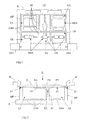
- This device D comprises firstly a metal base or Ceramic S (see Figure 1) with an external peripheral wall MP, closing on itself to delimit an enclosure, and at least one wall internal MI, secured to the peripheral wall MP and subdividing the enclosure into minus two cavities Ci.
- i is equal to six (6), but it can take anything which value is greater than or equal to two.
- the peripheral wall MP and the internal walls MI delimit together six cavities C1 to C6 in which are conventionally installed SEH hybrid subsystems each consisting of at least one hybrid circuit CHH microwave.
- SEH hybrid subsets can be coupled to each other via CX connections passing through the internal MI walls.
- the subassemblies SEH hybrids are coupled to external connection terminals CE1 and CE2, allowing the connection of the hybrid device D to equipment.
- peripheral walls MP and internal (s) MI protrude from the base S.
- Such an arrangement can be obtained in particular by machining a plate metal, usually in Kovar ®, or by brazing walls reported on a multilayer ceramic support or not, or by any other means making it possible to make cavities Ci.
- the hybrid device D comprises a metal cover C, usually in Kovar ® (see Figure 2), intended to be secured by its face internal FI at the end E1 of the peripheral wall MP.
- This solidarity for example by electric welding with the help of M. technique ensures a hermetic closure of the enclosure on the plan of the microwave, and establish a mass electrical contact between the hood C and the peripheral wall MP.
- the cover C In order to ensure the hermetic closure of the cavities Ci of the enclosure, on the plane of the microwave, and to establish a mass electrical contact between the C cover and internal walls MP, the cover C has, on its inner face FI, EC deformable contact means and elastic (and therefore flexible).
- the contact means EC are preferentially secured to the internal face FI of the cover C, in selected locations to allow the establishment of an electrical contact mass, elastic, between the cover C and each internal wall MI.
- the fastening of the EC contact means to the cover C by gold-tin welding (Au-Sn) or by electric welding points.
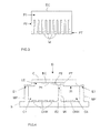
- the contact means EC are preferably arranged under the form of at least one insert having a first portion P1 secured to the inner face FI of the cover C and extended by a second part P2 deformable and elastic.
- This element is made of a material electrically conductive like for example beryllium copper.
- the cover C may comprise either an EC insert element of this type, or several, to allow the microwave shielding of each cavity Ci, or only some of them.
- the first part P1 of a reported element EC is for example arranged in the form of a strip plane and the second part P2, which prolongs this band, is example arranged in the form of at least two blades (or fingers) Lj deformable and elastic.
- j is equal to eleven (11), but he can take any value greater than or equal to two (2).
- Lj blades are particularly advantageous because they offer a high elasticity and withstand significant mechanical deformations. They can thus ensure a quality electrical contact of quality including in difficult operating conditions.
- the spacing between adjacent blades Lj is chosen according to the operating frequency band of microwave hybrid circuits CHH. It is indeed imperative that this spacing prohibit the passage of microwaves if it is desired to isolate the cavities Ci from each other, effective way.
- the hybrid device D can thus be used at least until K band (Ku as Ka).
- each blade Lj extends the P1 band according to an angle chosen according to, in particular, the height of the wall MI and the shape of the cover C. Furthermore, the terminal part PT of each blade Lj, opposite to the band P1, is preferentially conformed to to define a kind of bowl whose bottom is in contact with the end E2 of the internal wall MI concerned. This allows to get a contact between the blade Lj and the internal wall MI of a nature to minimize the risks abrasion may occur during relative movements between the blade Lj and the internal wall MI.
- the internal walls MI have a height less than the height of the peripheral wall MP and the internal face FI of the cover C is substantially flat at least in the region which is located next to cavities Ci. But it may be otherwise.
- the invention can indeed be applied, also, to S bases traditional in which the height of the MI internal walls is substantially equal to that of the peripheral wall MP.
- the cover C must be shaped so as to define at least one housing LE for receiving the EC contact means.
- the hood C can either include a single LE housing receiving all reported EC elements, ie several LE housing units each receiving at least an item reported.
- the housing (s) LE can be obtained by chemical machining a metal plate defining the cover C, or by any other means appropriate.
Landscapes
- Engineering & Computer Science (AREA)
- Microelectronics & Electronic Packaging (AREA)
- Shielding Devices Or Components To Electric Or Magnetic Fields (AREA)
- Constitution Of High-Frequency Heating (AREA)
- Casings For Electric Apparatus (AREA)
Abstract
Description
- un socle comprenant plusieurs murs internes. Dans ce cas, les moyens de contact sont agencés de manière à établir un contact électrique avec l'extrémité de chaque mur interne,
- des mur périphérique et mur(s) interne(s) faisant saillie du socle,
- des moyens de contact agencés sous la forme d'au moins un élément rapporté, par exemple solidarisé à la face interne du capot par soudage, et comportant une première partie solidarisée à la face interne du capot et prolongée par une seconde partie déformable et élastique. Par exemple, la première partie est en forme de bande et la seconde partie est constituée d'au moins deux lames déformables et élastiques (espacées d'une distance choisie en fonction de la bande de fréquence de fonctionnement desdits circuits hybrides hyperfréquences),
- chaque mur interne peut présenter une hauteur inférieure à celle du mur périphérique. Dans ce cas, la face interne du capot est sensiblement plane au moins dans la région située en regard des cavités. En variante, chaque mur interne peut présenter une hauteur sensiblement égale à la hauteur du mur périphérique. Dans ce cas, le capot est conformé de manière à définir au moins un logement propre à recevoir les moyens de contact. On peut même envisager que le capot comprenne autant de logements que d'éléments rapportés.
- la figure 1 illustre de façon schématique, dans une vue du dessus, un exemple de socle de dispositif hybride selon l'invention,
- la figure 2 illustre de façon schématique, dans une vue en coupe transversale, un premier exemple de réalisation d'un dispositif hybride selon l'invention,
- la figure 3 illustre de façon schématique, dans une vue du dessus, un exemple de réalisation d'un élément de contact d'un dispositif hybride selon l'invention, et
- la figure 4 illustre de façon schématique, dans une vue en coupe transversale, un second exemple de réalisation d'un dispositif hybride selon l'invention.
Claims (12)
- Dispositif (D) à circuits hybrides hyperfréquences (CHH) comprenant un socle (S) muni d'un mur périphérique externe (MP) et d'au moins un mur interne (MI) délimitant ensemble au moins deux cavités (Ci) propres à loger des circuits hybrides hyperfréquences (CHH), et un capot (C) propre à être solidarisé par une face interne (FI) à l'extrémité dudit mur périphérique (MP) de manière à assurer une fermeture hermétique des cavités (Ci) et à établir un contact électrique avec ledit mur périphérique (MP), caractérisé en ce que ledit capot (C) comporte des moyens de contact (EC) déformables et élastiques, solidarisés à sa face interne (FI), et agencés de manière à établir un contact électrique avec l'extrémité dudit mur interne (MI).
- Dispositif selon la revendication 1, caractérisé en ce que ledit socle (S) comprend plusieurs murs internes (MI) et en ce que lesdits moyens de contact (EC) sont agencés de manière à établir un contact électrique avec l'extrémité de chaque mur interne (MI).
- Dispositif selon l'une des revendications 1 et 2, caractérisé en ce que lesdits mur périphérique (MP) et mur(s) interne(s) (MI) font saillie dudit socle (S).
- Dispositif selon l'une des revendications 1 à 3, caractérisé en ce que lesdits moyens de contact (EC) sont agencés sous la forme d'au moins un élément rapporté comportant une première partie (P1) solidarisée à ladite face interne (FI) du capot (C) et prolongée par une seconde partie (P2) déformable et élastique.
- Dispositif selon la revendication 4, caractérisé en ce que ladite première partie (P1) est en forme de bande et ladite seconde partie (P2) est constituée d'au moins deux lames (L) déformables et élastiques.
- Dispositif selon la revendication 5, caractérisé en ce que lesdites lames (L) sont espacées d'une distance choisie en fonction de la bande de fréquence de fonctionnement desdits circuits hybrides hyperfréquences (CHH).
- Dispositif selon l'une des revendications 5 et 6, caractérisé en ce que chaque lame (L) comprend une partie terminale (PT) conformé de manière à définir une cuvette dont un fond est destiné à contacter l'extrémité du mur interne (MI).
- Dispositif selon l'une des revendications 1 à 7, caractérisé en ce que lesdits moyens de contact (EC) sont solidarisés à ladite face interne (FI) du capot (C).
- Dispositif selon l'une des revendications 1 à 8, caractérisé en ce que chaque mur interne (MI) présente une hauteur inférieure à la hauteur dudit mur périphérique (MP), et en ce que ladite face interne (FI) du capot (C) est sensiblement plane au moins dans une région en regard desdites cavités (Ci).
- Dispositif selon l'une des revendications 1 à 8, caractérisé en ce que chaque mur interne (MI) présente une hauteur sensiblement égale à la hauteur dudit mur périphérique (MP), et en ce que ledit capot (C) est conformé de manière à définir au moins un logement (LE) propre à recevoir lesdits moyens de contact (EC).
- Dispositif selon la combinaison des revendications 4 et 10, caractérisé en ce que ledit capot (C) comprend autant de logements (LE) que d'éléments (EC).
- Utilisation du dispositif (D) selon l'une des revendications précédentes dans des bandes de fréquence allant au moins jusque dans une bande de fréquence dite « bande K ».
Priority Applications (1)
| Application Number | Priority Date | Filing Date | Title |
|---|---|---|---|
| PL04291722T PL1498950T3 (pl) | 2003-07-18 | 2004-07-07 | Urządzenie ze scalonymi układami hybrydowymi o częstotliwości mikrofalowej z ekranowaniem przez zestykowy(e) element(y) sprężysty(e) |
Applications Claiming Priority (2)
| Application Number | Priority Date | Filing Date | Title |
|---|---|---|---|
| FR0308773 | 2003-07-18 | ||
| FR0308773A FR2857819B1 (fr) | 2003-07-18 | 2003-07-18 | Dispositif a circuits hybrides hyperfrequences a blindage par element(s)de contact elastique(s) |
Publications (2)
| Publication Number | Publication Date |
|---|---|
| EP1498950A1 true EP1498950A1 (fr) | 2005-01-19 |
| EP1498950B1 EP1498950B1 (fr) | 2008-12-31 |
Family
ID=33462558
Family Applications (1)
| Application Number | Title | Priority Date | Filing Date |
|---|---|---|---|
| EP04291722A Expired - Lifetime EP1498950B1 (fr) | 2003-07-18 | 2004-07-07 | Dispositif à circuits hybrides hyperfréquences à blindage par élèments(s) de contact élastiques(s) |
Country Status (10)
| Country | Link |
|---|---|
| US (1) | US7180393B2 (fr) |
| EP (1) | EP1498950B1 (fr) |
| JP (1) | JP2005123572A (fr) |
| AT (1) | ATE419649T1 (fr) |
| CA (1) | CA2472900A1 (fr) |
| DE (1) | DE602004018712D1 (fr) |
| DK (1) | DK1498950T3 (fr) |
| ES (1) | ES2320447T3 (fr) |
| FR (1) | FR2857819B1 (fr) |
| PL (1) | PL1498950T3 (fr) |
Families Citing this family (6)
| Publication number | Priority date | Publication date | Assignee | Title |
|---|---|---|---|---|
| KR100951266B1 (ko) | 2007-12-07 | 2010-04-02 | 삼성전기주식회사 | 세라믹 패키지 밀봉장치 |
| EP2398114A1 (fr) * | 2010-06-15 | 2011-12-21 | Research in Motion Limited | Composant de mise à la terre de doigt de ressort et procédé de fabrication |
| US20110306252A1 (en) * | 2010-06-15 | 2011-12-15 | Research In Motion Limited | Spring finger grounding component and method of manufacture |
| CN105304986A (zh) * | 2014-06-17 | 2016-02-03 | 中兴通讯股份有限公司 | 一种滤波器盖板、滤波器及滤波器盖板加工方法 |
| DE102016106135A1 (de) * | 2016-04-04 | 2017-10-05 | Vishay Semiconductor Gmbh | Elektronische Einheit |
| US11243675B1 (en) | 2021-02-12 | 2022-02-08 | Honda Motor Co., Ltd. | Method and system for enriching cross-brand user in interface experiences |
Citations (4)
| Publication number | Priority date | Publication date | Assignee | Title |
|---|---|---|---|---|
| JPH03268396A (ja) * | 1990-03-16 | 1991-11-29 | Fujitsu Ltd | マイクロ波回路筐体の遮蔽構造 |
| DE19609718C1 (de) * | 1996-03-13 | 1997-06-26 | Bosch Gmbh Robert | Hochfrequenzdichte Abschirmung |
| US20020074140A1 (en) * | 1997-07-05 | 2002-06-20 | Wolfgang Kuschke | Screening house for microwave circuits |
| JP2002299875A (ja) * | 2001-03-29 | 2002-10-11 | Sanyo Electric Co Ltd | シールドケース |
-
2003
- 2003-07-18 FR FR0308773A patent/FR2857819B1/fr not_active Expired - Fee Related
-
2004
- 2004-07-05 CA CA002472900A patent/CA2472900A1/fr not_active Abandoned
- 2004-07-07 DE DE602004018712T patent/DE602004018712D1/de not_active Expired - Fee Related
- 2004-07-07 DK DK04291722T patent/DK1498950T3/da active
- 2004-07-07 EP EP04291722A patent/EP1498950B1/fr not_active Expired - Lifetime
- 2004-07-07 ES ES04291722T patent/ES2320447T3/es not_active Expired - Lifetime
- 2004-07-07 PL PL04291722T patent/PL1498950T3/pl unknown
- 2004-07-07 AT AT04291722T patent/ATE419649T1/de not_active IP Right Cessation
- 2004-07-09 JP JP2004202720A patent/JP2005123572A/ja active Pending
- 2004-07-16 US US10/892,440 patent/US7180393B2/en not_active Expired - Fee Related
Patent Citations (4)
| Publication number | Priority date | Publication date | Assignee | Title |
|---|---|---|---|---|
| JPH03268396A (ja) * | 1990-03-16 | 1991-11-29 | Fujitsu Ltd | マイクロ波回路筐体の遮蔽構造 |
| DE19609718C1 (de) * | 1996-03-13 | 1997-06-26 | Bosch Gmbh Robert | Hochfrequenzdichte Abschirmung |
| US20020074140A1 (en) * | 1997-07-05 | 2002-06-20 | Wolfgang Kuschke | Screening house for microwave circuits |
| JP2002299875A (ja) * | 2001-03-29 | 2002-10-11 | Sanyo Electric Co Ltd | シールドケース |
Non-Patent Citations (2)
| Title |
|---|
| PATENT ABSTRACTS OF JAPAN vol. 016, no. 079 (E - 1171) 26 February 1992 (1992-02-26) * |
| PATENT ABSTRACTS OF JAPAN vol. 2003, no. 02 5 February 2003 (2003-02-05) * |
Also Published As
| Publication number | Publication date |
|---|---|
| EP1498950B1 (fr) | 2008-12-31 |
| PL1498950T3 (pl) | 2009-06-30 |
| FR2857819A1 (fr) | 2005-01-21 |
| DK1498950T3 (da) | 2009-04-14 |
| JP2005123572A (ja) | 2005-05-12 |
| CA2472900A1 (fr) | 2005-01-18 |
| DE602004018712D1 (de) | 2009-02-12 |
| ATE419649T1 (de) | 2009-01-15 |
| FR2857819B1 (fr) | 2008-11-28 |
| US7180393B2 (en) | 2007-02-20 |
| ES2320447T3 (es) | 2009-05-22 |
| US20050012574A1 (en) | 2005-01-20 |
Similar Documents
| Publication | Publication Date | Title |
|---|---|---|
| FR2860927A1 (fr) | Antenne interne de faible volume | |
| EP0995234A1 (fr) | Antenne a plaque | |
| FR3018989A1 (fr) | Module electronique, notamment pour un appareil de commande de boite de vitesses | |
| FR2660516A1 (fr) | Blindage electromagnetique pour circuit electrique. | |
| EP0113273A1 (fr) | Boîtier d'encapsulation pour semiconducteur de puissance, à isolement entrée-sortie amélioré | |
| EP3621093A1 (fr) | Bloc capacitif comprenant un dissipateur thermique | |
| EP1498950B1 (fr) | Dispositif à circuits hybrides hyperfréquences à blindage par élèments(s) de contact élastiques(s) | |
| FR2759843A1 (fr) | Dispositif de commande a monter dans un vehicule automobile | |
| FR2986657A1 (fr) | Entretoise de positionnement, module de stockage d'energie l'ayant et procede d'assemblage du module | |
| WO2003051095A1 (fr) | Module de puissance et ensemble de modules de puissance | |
| EP3888154A1 (fr) | Coffre de batterie et système de batterie modulaire | |
| EP2536261A1 (fr) | Module electronique de puissance a capacite integree | |
| EP2760708B1 (fr) | Sirene comportant un systeme de connexion ameliore | |
| EP3836765B1 (fr) | Module d'isolation électrique pour équipement électrique haute tension | |
| EP1460710A1 (fr) | Dispositif hyperfréquence destiné à la dissipation ou à l'atténuation de puissance | |
| EP1054445A1 (fr) | Boítier électronique sur plaque et procédé de fabrication d'un tel boítier | |
| EP0275772A1 (fr) | Boîtier de dispositif électrique, notamment de parafoudre, incluant une enveloppe isolante moulée | |
| CH694545A5 (fr) | Connecteur atténuateur d'hyperfréquences pour équipement logé dans un boîtier électromagnétiquement blindé et ensemble incluant un boîtier équipé d'un tel connecteur. | |
| EP2438651A1 (fr) | Dispositif de liaison entre un connecteur electrique et un cable electrique coaxial blinde et connecteur electrique correspondant | |
| FR2929048A1 (fr) | Ensemble de raccordement electrique et procede de fabrication de l'ensemble | |
| FR2928772A1 (fr) | Dispositif pour prevenir l'etablissement d'un arc electrique entre deux elements conducteurs. | |
| FR3015855A1 (fr) | Boiter pour carte electronique | |
| FR2697715A1 (fr) | Circuit imprimé double face et ensemble de conduction électrique comprenant un tel circuit imprimé. | |
| WO2026092999A1 (fr) | Boîtier d'unité de commande comportant un bouclier à éléments poussoirs à bras élastiques parallèles au bord | |
| FR2733351A1 (fr) | Connecteur interrupteur ou inverseur coaxial miniature a plongeur et lames de contact passives |
Legal Events
| Date | Code | Title | Description |
|---|---|---|---|
| PUAI | Public reference made under article 153(3) epc to a published international application that has entered the european phase |
Free format text: ORIGINAL CODE: 0009012 |
|
| AK | Designated contracting states |
Kind code of ref document: A1 Designated state(s): AT BE BG CH CY CZ DE DK EE ES FI FR GB GR HU IE IT LI LU MC NL PL PT RO SE SI SK TR |
|
| AX | Request for extension of the european patent |
Extension state: AL HR LT LV MK |
|
| 17P | Request for examination filed |
Effective date: 20050719 |
|
| AKX | Designation fees paid |
Designated state(s): AT BE BG CH CY CZ DE DK EE ES FI FR GB GR HU IE IT LI LU MC NL PL PT RO SE SI SK TR |
|
| RAP1 | Party data changed (applicant data changed or rights of an application transferred) |
Owner name: ALCATEL LUCENT |
|
| 17Q | First examination report despatched |
Effective date: 20070705 |
|
| GRAP | Despatch of communication of intention to grant a patent |
Free format text: ORIGINAL CODE: EPIDOSNIGR1 |
|
| GRAS | Grant fee paid |
Free format text: ORIGINAL CODE: EPIDOSNIGR3 |
|
| GRAA | (expected) grant |
Free format text: ORIGINAL CODE: 0009210 |
|
| AK | Designated contracting states |
Kind code of ref document: B1 Designated state(s): AT BE BG CH CY CZ DE DK EE ES FI FR GB GR HU IE IT LI LU MC NL PL PT RO SE SI SK TR |
|
| REG | Reference to a national code |
Ref country code: CH Ref legal event code: EP Ref country code: GB Ref legal event code: FG4D Free format text: NOT ENGLISH |
|
| REF | Corresponds to: |
Ref document number: 602004018712 Country of ref document: DE Date of ref document: 20090212 Kind code of ref document: P |
|
| REG | Reference to a national code |
Ref country code: IE Ref legal event code: FG4D Free format text: LANGUAGE OF EP DOCUMENT: FRENCH |
|
| REG | Reference to a national code |
Ref country code: RO Ref legal event code: EPE |
|
| REG | Reference to a national code |
Ref country code: SE Ref legal event code: TRGR |
|
| REG | Reference to a national code |
Ref country code: DK Ref legal event code: T3 |
|
| REG | Reference to a national code |
Ref country code: ES Ref legal event code: FG2A Ref document number: 2320447 Country of ref document: ES Kind code of ref document: T3 |
|
| PG25 | Lapsed in a contracting state [announced via postgrant information from national office to epo] |
Ref country code: FI Free format text: LAPSE BECAUSE OF FAILURE TO SUBMIT A TRANSLATION OF THE DESCRIPTION OR TO PAY THE FEE WITHIN THE PRESCRIBED TIME-LIMIT Effective date: 20081231 Ref country code: SI Free format text: LAPSE BECAUSE OF FAILURE TO SUBMIT A TRANSLATION OF THE DESCRIPTION OR TO PAY THE FEE WITHIN THE PRESCRIBED TIME-LIMIT Effective date: 20081231 |
|
| REG | Reference to a national code |
Ref country code: PL Ref legal event code: T3 |
|
| PG25 | Lapsed in a contracting state [announced via postgrant information from national office to epo] |
Ref country code: EE Free format text: LAPSE BECAUSE OF FAILURE TO SUBMIT A TRANSLATION OF THE DESCRIPTION OR TO PAY THE FEE WITHIN THE PRESCRIBED TIME-LIMIT Effective date: 20081231 |
|
| PG25 | Lapsed in a contracting state [announced via postgrant information from national office to epo] |
Ref country code: PT Free format text: LAPSE BECAUSE OF FAILURE TO SUBMIT A TRANSLATION OF THE DESCRIPTION OR TO PAY THE FEE WITHIN THE PRESCRIBED TIME-LIMIT Effective date: 20090601 Ref country code: CZ Free format text: LAPSE BECAUSE OF FAILURE TO SUBMIT A TRANSLATION OF THE DESCRIPTION OR TO PAY THE FEE WITHIN THE PRESCRIBED TIME-LIMIT Effective date: 20081231 Ref country code: AT Free format text: LAPSE BECAUSE OF FAILURE TO SUBMIT A TRANSLATION OF THE DESCRIPTION OR TO PAY THE FEE WITHIN THE PRESCRIBED TIME-LIMIT Effective date: 20081231 |
|
| PG25 | Lapsed in a contracting state [announced via postgrant information from national office to epo] |
Ref country code: SK Free format text: LAPSE BECAUSE OF FAILURE TO SUBMIT A TRANSLATION OF THE DESCRIPTION OR TO PAY THE FEE WITHIN THE PRESCRIBED TIME-LIMIT Effective date: 20081231 |
|
| PLBE | No opposition filed within time limit |
Free format text: ORIGINAL CODE: 0009261 |
|
| STAA | Information on the status of an ep patent application or granted ep patent |
Free format text: STATUS: NO OPPOSITION FILED WITHIN TIME LIMIT |
|
| 26N | No opposition filed |
Effective date: 20091001 |
|
| PG25 | Lapsed in a contracting state [announced via postgrant information from national office to epo] |
Ref country code: BG Free format text: LAPSE BECAUSE OF FAILURE TO SUBMIT A TRANSLATION OF THE DESCRIPTION OR TO PAY THE FEE WITHIN THE PRESCRIBED TIME-LIMIT Effective date: 20090331 |
|
| BERE | Be: lapsed |
Owner name: ALCATEL LUCENT Effective date: 20090731 |
|
| PG25 | Lapsed in a contracting state [announced via postgrant information from national office to epo] |
Ref country code: MC Free format text: LAPSE BECAUSE OF NON-PAYMENT OF DUE FEES Effective date: 20090731 |
|
| REG | Reference to a national code |
Ref country code: CH Ref legal event code: PL |
|
| REG | Reference to a national code |
Ref country code: DK Ref legal event code: EBP |
|
| EUG | Se: european patent has lapsed | ||
| GBPC | Gb: european patent ceased through non-payment of renewal fee |
Effective date: 20090707 |
|
| NLV4 | Nl: lapsed or anulled due to non-payment of the annual fee |
Effective date: 20100201 |
|
| REG | Reference to a national code |
Ref country code: FR Ref legal event code: ST Effective date: 20100331 |
|
| REG | Reference to a national code |
Ref country code: IE Ref legal event code: MM4A |
|
| PG25 | Lapsed in a contracting state [announced via postgrant information from national office to epo] |
Ref country code: LI Free format text: LAPSE BECAUSE OF NON-PAYMENT OF DUE FEES Effective date: 20090731 Ref country code: CH Free format text: LAPSE BECAUSE OF NON-PAYMENT OF DUE FEES Effective date: 20090731 Ref country code: FR Free format text: LAPSE BECAUSE OF NON-PAYMENT OF DUE FEES Effective date: 20090731 |
|
| PG25 | Lapsed in a contracting state [announced via postgrant information from national office to epo] |
Ref country code: GB Free format text: LAPSE BECAUSE OF NON-PAYMENT OF DUE FEES Effective date: 20090707 |
|
| PG25 | Lapsed in a contracting state [announced via postgrant information from national office to epo] |
Ref country code: DE Free format text: LAPSE BECAUSE OF NON-PAYMENT OF DUE FEES Effective date: 20100202 Ref country code: BE Free format text: LAPSE BECAUSE OF NON-PAYMENT OF DUE FEES Effective date: 20090731 |
|
| PG25 | Lapsed in a contracting state [announced via postgrant information from national office to epo] |
Ref country code: DK Free format text: LAPSE BECAUSE OF NON-PAYMENT OF DUE FEES Effective date: 20090731 Ref country code: IE Free format text: LAPSE BECAUSE OF NON-PAYMENT OF DUE FEES Effective date: 20090707 |
|
| REG | Reference to a national code |
Ref country code: ES Ref legal event code: FD2A Effective date: 20090708 |
|
| PG25 | Lapsed in a contracting state [announced via postgrant information from national office to epo] |
Ref country code: GR Free format text: LAPSE BECAUSE OF FAILURE TO SUBMIT A TRANSLATION OF THE DESCRIPTION OR TO PAY THE FEE WITHIN THE PRESCRIBED TIME-LIMIT Effective date: 20090401 Ref country code: ES Free format text: LAPSE BECAUSE OF NON-PAYMENT OF DUE FEES Effective date: 20090708 |
|
| PG25 | Lapsed in a contracting state [announced via postgrant information from national office to epo] |
Ref country code: RO Free format text: LAPSE BECAUSE OF NON-PAYMENT OF DUE FEES Effective date: 20081231 |
|
| PG25 | Lapsed in a contracting state [announced via postgrant information from national office to epo] |
Ref country code: IT Free format text: LAPSE BECAUSE OF NON-PAYMENT OF DUE FEES Effective date: 20090707 |
|
| PG25 | Lapsed in a contracting state [announced via postgrant information from national office to epo] |
Ref country code: LU Free format text: LAPSE BECAUSE OF NON-PAYMENT OF DUE FEES Effective date: 20090707 |
|
| PG25 | Lapsed in a contracting state [announced via postgrant information from national office to epo] |
Ref country code: SE Free format text: LAPSE BECAUSE OF NON-PAYMENT OF DUE FEES Effective date: 20090708 Ref country code: PL Free format text: LAPSE BECAUSE OF NON-PAYMENT OF DUE FEES Effective date: 20090707 |
|
| PG25 | Lapsed in a contracting state [announced via postgrant information from national office to epo] |
Ref country code: HU Free format text: LAPSE BECAUSE OF FAILURE TO SUBMIT A TRANSLATION OF THE DESCRIPTION OR TO PAY THE FEE WITHIN THE PRESCRIBED TIME-LIMIT Effective date: 20090701 |
|
| REG | Reference to a national code |
Ref country code: PL Ref legal event code: LAPE |
|
| PG25 | Lapsed in a contracting state [announced via postgrant information from national office to epo] |
Ref country code: CY Free format text: LAPSE BECAUSE OF FAILURE TO SUBMIT A TRANSLATION OF THE DESCRIPTION OR TO PAY THE FEE WITHIN THE PRESCRIBED TIME-LIMIT Effective date: 20081231 |
|
| PG25 | Lapsed in a contracting state [announced via postgrant information from national office to epo] |
Ref country code: NL Free format text: LAPSE BECAUSE OF NON-PAYMENT OF DUE FEES Effective date: 20100201 |
|
| PG25 | Lapsed in a contracting state [announced via postgrant information from national office to epo] |
Ref country code: TR Free format text: LAPSE BECAUSE OF FAILURE TO SUBMIT A TRANSLATION OF THE DESCRIPTION OR TO PAY THE FEE WITHIN THE PRESCRIBED TIME-LIMIT Effective date: 20081231 |
|
| REG | Reference to a national code |
Ref country code: FR Ref legal event code: CA Effective date: 20150521 |
|
| REG | Reference to a national code |
Ref country code: FR Ref legal event code: CA Effective date: 20150521 |