This application is based upon and claims the
benefit of priority from the prior Japanese Patent
Application No. 2002-114950, filed April 17, 2002,
the entire contents of which are incorporated herein by
reference.
Technical Field
The present invention relates to a signal
detection contactor and signal calibration system used
when calibrating a signal for testing the electrical
characteristics of, e.g., a high-speed device.
Background Art
In the manufacturing process for a semiconductor
device or the like, when testing the electrical
characteristics of a target test object (to be referred
to as "device" hereinafter) formed on a wafer-like
substrate (to be merely referred to as "wafer"
hereinafter) W, a prober shown in, e.g., FIGS. 4A and
4B, is used. The prober has a loader chamber 1 and
prober chamber 2. A test head T for a tester 27 is
pivotally arranged on a head plate 9 arranged on the
prober chamber 2. The test head T is electrically
connected to a probe card 7 and a plurality of probes
7A provided to the probe card through a performance
board (not shown). A test signal transmitted from the
tester 27 is sent to the probes 7A through the test
head T and the performance board. The probes 7A apply
test signals to the electrode pads of a device formed
on the wafer W. Thus, the electrical characteristics
of the device, e.g., a plurality of semiconductor
devices (chips), formed on the wafer W are tested.
The test signals are transmitted from the tester
27 to the probes 7A through signal lines. If all the
signal lines and the probes 7A have the same physical
characteristics, the test signals can be correctly
transmitted to the plurality of probes 7A through the
performance board. Therefore, the probes 7A can apply
the test signals to the electrode pads with the same
phase, so that the device can be tested correctly. Due
to a slight difference in the manufacturing process,
however, sometimes the physical characteristics of the
respective signal lines and the respective probes 7A
differ slightly from each other. As the test signals
are very sensitive, a slight difference in physical
characteristics of the probes 7A may sometimes cause,
e.g., a phase difference, among the test signals that
have arrived the distal ends of the probes 7A. If the
test signals have a phase difference or the like, it is
difficult to correctly test the device.
As a technique for calibrating the phase
difference of the signals, for example, Jpn. Pat.
Appln. KOKAI Publication No. 2000-352578 discloses
a technique related to a timing calibration method for
an IC test device. According to the timing calibration
method described in Jpn. Pat. Appln. KOKAI Publication
No. 2000-352578, delay time difference among signals
from times at the signal generation to times at the
signal arrival due to difference in the length of
signal transmission lines of the IC test device can be
calibrated. Due to the manufacturing process or
the like, however, if the physical characteristics of
the signal lines or the like differ slightly, and
accordingly the timings at which signals of the
respective signal lines arrive differ, this difference
in timing cannot be calibrated. This timing
calibration method is concerned with an IC test device.
In the prober, the arrival times of signals, which
transmitted from the tester to the probe card, differ
depending on the physical characteristics of the
respective signal lines. It is recognized that, in
order to calibrate the arrival times of the respective
signals, the signals must be detected at the distal
ends of the respective probes. It is, however,
difficult to detect the signals at the distal ends of
the probes, and accordingly it is difficult to detect
and calibrate the difference among the plurality of
test signals.
Disclosure of Invention
The invention of the present application has been
made to solve at least one of the problems described
above. According to one aspect of the present
invention, there is provided a signal detection
contactor which can reliably detect a signal from the
distal end of a probe. According to another aspect of
the present invention, there is provided a signal
detection contactor which has excellent RF characteristics
and can obtain a stable contact state with
a probe.
According to a further aspect of the present
invention, there is provided a signal calibration
system which can detect and calibrate signals from
the distal end of probes.
The further problems and advantages of the present
invention will be described hereinafter, part of which
is obvious from the disclosure thereof, or will become
apparent by practicing the present invention. The
objects and advantages of the present invention can be
realized by means particularly indicated herein and
a combination thereof.
According to the first aspect of the present
invention, there is provided, in an apparatus which
applies a signal from a signal source to a target
through at least one terminal, a signal detection
contactor to receive and detect the signal to be
applied by the terminal to an electrode of the target
by coming into contact with the terminal.
The signal detection contactor based on the first
aspect of the present invention can comprise either
one of the following preferable arrangements (1) to
(9), or a combination of any plurality of the following
arrangements.
According to another aspect of the present
invention, in a prober which transmits signals through
a plurality of probes to test electrical characteristics
of a target test object, there is provided,
a signal calibration system to calibrate a signal
applied by at least one probe on an electrode of the
target test object. The signal calibration system
based on this another aspect of the present invention
can further comprise at least one of the following
preferred arrangements (1) to (11), or an arrangement
as a combination of any plurality of the following
arrangements.
According to another aspect of the present
invention, there is provided, in a prober which
transmits signals through a plurality of probes to test
electrical characteristics of a target test object,
a method of calibrating a test signal in a signal
calibration system to calibrate a signal applied by at
least one probe to an electrode of the target test
object. This method comprises the following. (a) At
least one probe and at least one core wire of a coaxial
body provided to a signal detection contactor are
brought into contact with each other. (b) A signal
is transmitted from a tester provided to the prober
to a probe which is in contact with a core wire.
(c) The signal transmitted to the probe is applied
to the core which is in contact with the probe.
(d) The signal applied to the core wire is transmitted
to the tester. (e) The signal applied to the core wire
and transmitted to the tester is calibrated by the
tester. (f) The steps (b) to (e) are repeatedly
performed to calibrate signals transmitted to the other
probes.
Brief Description of Drawings
The accompanying drawings are incorporated in and
form a part of the specification to show a preferable
embodiment of the present invention. The drawings are
used in the description of the present invention by way
of general description made above and a detailed
description concerning the preferable embodiment to be
described below.
Best Mode for Carrying Out the Invention
The invention of the present application provides,
in an apparatus which applies a signal from a signal
source to a target through at least one terminal,
a signal detection contactor to receive and detect the
signal to be applied by the terminal to the electrode
of the target by coming into contact with the terminal,
and a signal calibration system and a method of
calibrating a signal to calibrate the signal applied
to the target. Various types of apparatuses are used
as the apparatus which applies a signal to a target.
To describe the invention of the present application
more specifically, a prober which tests the electrical
characteristics of a device will be described.
The signal calibration system according to the
invention of the present application will be described
by way of the embodiment shown in FIGS. 1 to 3.
In this embodiment, the signal detection contactor and
the method of calibrating a signal according to an
embodiment of the invention of the present application
will also be described. As shown in FIG. 1, a signal
calibration system 10 according to this embodiment
detects and calibrates a signal for testing a device
in a prober 20. The signal calibration system 10 can
use a signal detection contactor 12 described above.
The prober 20 has an elevatable stage (e.g. main chuck)
22 in a prober chamber 21. The stage 22 can horizontally
move in X and Y directions by an X-Y table 23.
A probe card 24 is arranged above the stage 22. The
probe card 24 can be electrically connected to a test
head 26 through a performance board 25. The test head
26 can also be connected to a tester 27. The probe
card 24, performance board 25, test head 26, and tester
27 can be electrically connected to each other through
50 Ω coaxial cables 28. When testing a wafer, an
alignment mechanism (not shown) and the X-Y table 23
cooperate with each other to align the electrode pads
of a device formed on the wafer placed on the stage 22
with probes 24A provided to the probe card 24. After
that, the stage 22 moves upward in the Z direction.
The electrode pads of the wafer and the probes 24A
are brought into electrical contact with each other.
The electrical characteristics of the wafer are
tested based on a plurality of test signals from the
tester 27.
The signal calibration system 10 according to this
embodiment may comprise the signal detection contactor
(to be merely referred to as "contactor" hereinafter)
12, the signal calibration unit 27 for calibrating
the signals, an elevating mechanism (e.g., elevating
cylinder) 11 added to the X-Y table 23, and a signal
detection body (to be referred to as "signal detection
board" hereinafter) 13.
The contactor 12 is fixed on a support 11A at the
upper end of the rod of the elevating cylinder 11, and
can come into electrical contact with the probes 24A of
the probe card 24. The signal detection board 13 can
be electrically connected to the contactor 12, and to
the signal calibration unit through a connector 14.
The signal calibration unit 27 outputs signals
to the probes through the test head 26. The signal
detection board 13 obtains the waveforms of the signals
through the contactor in electrical contact with the
probes. Hence, delay times and voltage levels of the
signals can be detected.
The signal detection board 13 can also have the
function of outputting signals. When the signal
detection board 13 outputs signals, the test head 26
serves as a signal detection board.
The signal calibration unit 27 calibrates, e.g.,
the levels and waveforms of the signals and a phase
difference among the signals. In this embodiment,
a tester is used as the signal calibration unit 27,
but the present invention is not limited to this.
The signal calibration unit 27 may be provided
independently of the tester, or can be built into the
tester. In the following description, the signal
calibration unit 27 serves as the tester 27. The
contactor 12, signal detection board 13, connector 14,
and tester 27 can be connected to each other through
50Ω coaxial cables 29.
FIG. 1 is a view in which the contactor 12 is in
contact with the probes 24A. When testing the wafer,
the upper surface of the contactor 12 can be set at
a position lower than the wafer stage surface of the
stage 22, so it will not hinder wafer test.
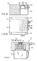
As shown in, e.g., FIGS. 2A and 2B, the contactor
12 of this embodiment can have a contactor main body
121, and at least one coaxial body 122 provided to
the contactor main body 121. The coaxial body 122 can
comprise a core wire 122A. When the core wire 122A
comes into contact with a corresponding probe 24A,
a test signal arriving the distal end of the probe 24A
can be received. The signal received by the core wire
122A can be transmitted to the tester 27 through the
signal detection board 13 and connector 14 shown in
FIG. 1. The tester 27 can calibrate the phase
differences among the plurality of signals transmitted
to it. The tester 27 can also calibrate the waveforms
and signal levels of the respective signals.
As shown in FIG. 2, the contactor main body 121
can be made of, e.g., a metal. In this embodiment,
a rectangular structure made of an iron alloy is
employed. One or a plurality of coaxial bodies 122 can
be provided to the contactor 12. The contactor of this
embodiment has three coaxial bodies. The three coaxial
bodies 122 are used as a driver coaxial body, a
comparator coaxial body, and a waveform monitor coaxial
body, respectively. The plurality of coaxial bodies
122 can be arranged in the contactor main body 121
with a layout different from that of the plurality
of probes. In this embodiment, the coaxial bodies 122
can be arranged obliquely on one side surface of the
contactor main body 121, as shown in FIG. 2B. When the
coaxial bodies 122 have an oblique layout, they can be
shifted from the layout of the probes 24A. If the
layout of the coaxial bodies and the layout of the
probes are shifted from each other, when one coaxial
body 122 is in contact with one probe 24A, the other
coaxial bodies 122 can be prevented from coming into
contact with the other probes 24A.
The core wire 122A provided to the coaxial body
122 of FIG. 3 has its upper end face 122G exposed at
least at one portion of the surface of the contactor
main body, so that it can come into contact with the
corresponding probe 24A. The position of the core wire
122A is not limited to this, and the core wire 122A
can be arranged at any position where it can come
into contact with the corresponding probe 24A on the
contactor.
When a test signal deriving portion is formed as
the coaxial body 122, a contactor 12 having excellent
frequency characteristics with which even a high
frequency will not attenuate easily can be provided.
Consequently, even an RF signal can be calibrated
reliably. The flat surface of the contactor main body
121 can have a size of, e.g., a 40-mm square.
A cutout portion 121A can be formed in one side
surface (right surface in FIGS. 2A and 2B) of the
contactor main body 121. A plate-like portion 121B can
be formed on the upper side of the cutout portion 121A.
For example, the three coaxial bodies 122 can be buried
in the plate-like portion 121B. The cutout portion
121A can accommodate coaxial connectors 124 connected
to the coaxial bodies 122. When a cutout portion is
formed in the contactor main body, coaxial bodies and
the like can be arranged easily. Flanges 121C are
formed on the left and right of (top and bottom in
FIG. 2B) the contactor main body 121. The contactor
main body 121 can be fixed to the support 11A of the
elevating cylinder 11 through the flanges 121C.
The contactor can have a conductor surface 125
with which at least part of a probe other than the
probe which comes into contact with the core wire
122A comes into contact. The conductor surface 125
can be formed by, e.g., nickel plating performed on
the surface of the contactor main body 121. Thus,
impedance matching can be performed between the probe
24A in contact with the core wire 122A and a probe 24A
in contact with the nickel-plated 125 portion.
The signals are transmitted from the tester 27
to the probe card 24 through the coaxial cables 28.
However, the probes 24A themselves cannot have coaxial
structures. Therefore, when the signals are
transmitted from the probe card 24, signal reflection
may occur on the distal ends of the probes 24A due to
impedance mismatching, causing disturbance in the
signal waveforms. Concerning this, according to
the present invention, a test signal probe 24A and
a ground probe 24B can be arranged on the probe card
24. The ground probe 24B of the coaxial cable 28 can
be arranged adjacent to the test signal probe 24 of the
coaxial cable 28 corresponding to this ground probe
24B. Therefore, when the signal probe 24A comes into
contact with the upper end face 122G of the core wire
122A provided to the contactor main body 121, the
ground probe 24B comes into contact with the nickel-plated
portion of the contactor main body 121
simultaneously. Thus, an impedance of 50Ω can be
maintained in the entire signal transmission lines, and
signal reflection or the like from the distal ends of
the other probes 24A (probes other than the probe 24A
in contact with the contactor 12) can be prevented.
That surface of the contactor main body 121 with which
the other probes 24A come into contact is grounded
to the ground of the coaxial connectors 124 connected
from the contactor main body 121 to the tester 27.
Thus, signals can be detected more correctly.
FIG. 3 is an enlarged sectional view of the
buried portion of the coaxial body 122 in FIG. 2A.
This coaxial body 122 may have the core wire 122A,
an insulating layer 122B, and a conductor layer 122C.
The insulating layer 122B covers the outer surface of
the core wire 122A. The conductor layer 122C covers
the outer surface of the insulating layer 122B.
Part of the core wire 122A can have a projection 122D
projecting upward from the upper ends of the insulating
layer 122B and conductor layer 122C. This core wire
has the upper end face 122G to come into contact with
the probe, and the main body portion 122A continuous to
the upper end face. The diameter of the upper end face
122G can be smaller than that of the main body portion.
For example, the projection 122D of the core wire 122A
can be comprised of a tapered portion 122E and small-diameter
portion 122F. The diameter of the tapered
portion 122E gradually decreases upward. The small-diameter
portion 122F projects from the tapered portion
122E toward the upper end. In this embodiment, the
projection 122D, i.e., the upper end face 122G of the
core wire 122A, can be formed, e.g., with a diameter of
80 µm corresponding to the size of the electrode pad
of the wafer. In this manner, since the upper end face
122G of the core wire to come into contact with the
probe can have a desired diameter, the upper end face
122G can be formed in accordance with the density of
the probes 24A.
Furthermore, the contactor main body 121 can
have an insulator 123 for covering the outer surface
of the upper end face 122G of the core wire to come
into contact with the probe 24A. For example, the
projection 122D can be covered with the insulator 123
on the surface layer portion of the plate-like portion
121B. When the upper end face 122G of the core wire
122A is covered with the insulator 123, the probe 24A
to come into contact with the core wire 122A and
a probe 24A adjacent to it can be electrically
insulated from each other reliably. The insulator 123
can be provided to share the axis with the tapered
portion 122E. The surfaces of the projection 122D
and insulator 123 can be flush with the plate-like
portion 121B.
The core wire 122A can be made of an ultrafine-particle
hard metal, and can be made of, e.g., tungsten
carbide. The insulator 123 can be made of an
insulating material such as glass. Since the core wire
122A is made of an ultrafine-particle hard metal, it is
resistant against wear by contact with the probe 24A,
thus providing a structure with excellent durability.
Furthermore, the upper end face 122G of the
core wire 122A to come into contact with the probe
on the surface of the contactor main body can be
dull-finished. Then, the upper end face 122G of the
core wire reliably grips the needle point of the probe
24A, so that a stable contact state can be obtained.
The operation will be described. Prior to wafer
test using the prober 20, the test signal used
for wafer test is calibrated by using the signal
calibration system 10. For this purpose, first, the
position coordinates of the three core wires 122A on
the contactor 12 fixed to the elevating cylinder 11 are
input as initial setting. In this case, the images of
the core wires which can be sensed by a camera provided
for the alignment mechanism (not shown) of the prober,
can be input, or can be directly. input by using a ten-key
pad. Subsequent to the position coordinates of the
core wires, the position coordinates of the plurality
of probes 24A are input. In this case as well, the
position coordinates can be input by using the camera
provided to the alignment mechanism, or can be directly
input by using the ten-key pad or the like. After this
initial setting is ended, the position information of
the probes 24A and core wires 122A are transmitted to
the prober 20.
In the prober 20, the alignment mechanism brings
the specified probes 24A and specified core wires 122A
in contact with each other based on these pieces of
information. More specifically, the X-Y table 23 moves
the contactor 12 in the X or Y direction, to align the
upper end faces 122G of the core wires provided to the
coaxial bodies 122, and the probes 24A with each other.
Subsequently, the elevating cylinder 11 moves the
contactor 12 upward to be higher than the stage surface
of the stage 22. Then, as shown in FIG. 1, the upper
end faces 122G of the core wires and the needle points
of the probes 24A can come into contact with each
other. At this time, when the upper end faces 122G of
the core wires 122A are dull-finished, a stable contact
state can be obtained between the needle points of the
probes 24A and the upper end faces 122G of the core
wires 122A. Thus, contact between the needle points
of the probes 24A and the upper end faces 122G of the
core wires 122A is stabilized, and the core wires 122A
can reliably receive the signals from the probes 24A.
At this time, the probe 24A for applying a driver test
signal can come into contact with the driver core wire
122A. The probe 24A for applying a comparator test
signal can come into contact with the comparator core
wire 122A.
With the core wires 122A and the probes 24A being
in contact with each other, the tester 27 transmits
predetermined test signals to the probe card 24.
The test signals arrive the probes 24A through the
respective signal wires of the test head 26 and
performance board 25, and are applied to the core
wires 122A from the probes 24A. The signals received
by the contactor 12 are detected by the signal
detection board 13, and are transmitted to the tester
27. Alternatively, the signals received by the
contactor 12 may be directly transmitted to the
tester 27 and detected by it. The test signals are
transmitted through the coaxial bodies 122 in the
contactor 12. Thus, even if the signals arriving
the probe card 24 are RF test signals, they can be
correctly transmitted to the tester 27. The tester 27
measures the time taken from transmission to reception
of the test signals, and analyzes the waveforms and
signal levels of the received test signals, so that the
respective signals can be calibrated.
When signal analysis for one probe 24A is ended,
the tester 27 repeats measurement described above for
all the remaining probes 24A. The tester 27 compares
the arrival times of all the test signals taken from
transmission to reception, and refers to, e.g., that
test signal which has the longest arrival time, as a
reference, to equalize the arrival times of the other
test signals, so that the phase difference among the
signals can be calibrated. Alternatively, the tester
27 may refer to the arrival time of a desired signal
to calibrate the other signals. In this manner, the
phases of all test signals can be equalized.
The present invention is not limited to the above
embodiment at all. For example, it suffices as far as
the contactor 12 has at least one coaxial body 122.
The number of coaxial bodies can be increased as
necessary. As the material of the core wire 122A,
an ultrafine-particle hard metal other than tungsten
carbide can be used. To form the insulator 123
surrounding the core wire 122A, an insulating material
other than glass can be used.
According to the embodiment of the invention of
the present application, a signal at the distal end
of a probe is detected by using a signal detection
contactor. With this arrangement, a difference
in signal arrival times caused by a variation in
electrical characteristics of the respective signal
lines and respective probes due to a variation in
the manufacturing process can be detected reliably.
Thus, a signal calibration system that can correctly
calibrate a signal used for device measurement can be
provided.
According to the embodiment of the invention of
the present application, because of the presence of the
coaxial body, a signal detection contactor which has
excellent RF characteristics and can measure a signal
correctly and reliably can be provided.
According to the embodiment of the invention of
the present application, since the signal detection
contactor has a conductor surface, impedance matching
can be obtained between a probe in contact with the
coaxial body and a probe in contact with the contactor
surface.
According to the embodiment of the invention of
the present application, since a signal detection
contactor and a signal calibration unit are provided,
a phase difference among test signals can be detected
and calibrated precisely.
According to the embodiment of the invention of
the present application, since the plurality of coaxial
bodies are arranged in the contactor with a layout
different from that of the plurality of probes, a probe
other than the target probe can be prevented from
coming into contact with the coaxial body, and the
signal of the target probe can be measured precisely.
According to the embodiment of the invention of
the present application, the core wire provided to the
coaxial body has its upper end face exposed at least at
one portion of the surface of the contactor main body,
so that it can come into contact with the corresponding
probe. The upper end face of the core wire and the
conductor surface can form one flat surface. Thus, the
probe as the measurement target can come into contact
with the upper end face, while the other probes can
come into contact with the conductor surface.
According to the embodiment of the invention
of the present application, an insulator covers the
outer surface of the upper end face of the core wire.
Thus, a probe in contact with the core wire and a probe
adjacent to it can be electrically insulated from each
other reliably.
According to the embodiment of the invention of
the present application, the core wire is made of
an ultrafine-particle hard metal. Thus, a core wire
which is resistant against wear due to contact with the
probe and has excellent durability can be provided.
According to the embodiment of the invention of
the present application, the diameter of the core wire
decreases from its main body portion toward its upper
end face. Thus, the upper end face of the core wire
can have a desired diameter in accordance with the
density of the probes.
The upper end face of the core wire to come into
contact with the probe is dull-finished. Thus, a core
wire that can reliably grip the needle point of the
probe and accordingly can obtain a stable contact state
can be provided.
Further features and modifications are easily
anticipated by a person skilled in the art. Therefore,
the present invention has a wider perspective, and is
not limited to the specific detailed description and
typical embodiment disclosed herein. Accordingly,
various modifications can be made without departing
from the spirit and scope of the general idea of the
invention defined by the appended claims and an
equivalent thereof.