EP1498727A1 - Method for inspecting semiconductor device - Google Patents
Method for inspecting semiconductor device Download PDFInfo
- Publication number
- EP1498727A1 EP1498727A1 EP04015767A EP04015767A EP1498727A1 EP 1498727 A1 EP1498727 A1 EP 1498727A1 EP 04015767 A EP04015767 A EP 04015767A EP 04015767 A EP04015767 A EP 04015767A EP 1498727 A1 EP1498727 A1 EP 1498727A1
- Authority
- EP
- European Patent Office
- Prior art keywords
- wafer
- current
- change
- semiconductor device
- electromotive force
- Prior art date
- Legal status (The legal status is an assumption and is not a legal conclusion. Google has not performed a legal analysis and makes no representation as to the accuracy of the status listed.)
- Granted
Links
Images



Classifications
-
- G—PHYSICS
- G01—MEASURING; TESTING
- G01R—MEASURING ELECTRIC VARIABLES; MEASURING MAGNETIC VARIABLES
- G01R31/00—Arrangements for testing electric properties; Arrangements for locating electric faults; Arrangements for electrical testing characterised by what is being tested not provided for elsewhere
- G01R31/28—Testing of electronic circuits, e.g. by signal tracer
- G01R31/302—Contactless testing
- G01R31/308—Contactless testing using non-ionising electromagnetic radiation, e.g. optical radiation
- G01R31/311—Contactless testing using non-ionising electromagnetic radiation, e.g. optical radiation of integrated circuits
-
- H—ELECTRICITY
- H10—SEMICONDUCTOR DEVICES; ELECTRIC SOLID-STATE DEVICES NOT OTHERWISE PROVIDED FOR
- H10P—GENERIC PROCESSES OR APPARATUS FOR THE MANUFACTURE OR TREATMENT OF DEVICES COVERED BY CLASS H10
- H10P74/00—Testing or measuring during manufacture or treatment of wafers, substrates or devices
Definitions
- the present invention relates to a method and an apparatus for observing, analyzing, and inspecting a crystal defect which are suitable for use in analysis and inspection of a crystal defect, a junction breakage caused by an electric stress, or the like inside a wafer in which semiconductor device chips, in particular, compound-semiconductor laser diode device chips are integrated.
- a typical compound-semiconductor laser diode device mainly includes the laser diode chips in which a stacked structure made of several kinds of semiconductors is formed.
- An oscillator (stripe) is provided in the laser diode chip.
- the oscillator confines laser light and amplifies the laser light by resonance.
- Many technologies have been developed for failure analysis and inspection of the compound-semiconductor laser diode (hereinafter referred to as laser diode).
- the inspection of the laser diode includes an electrical and optical characteristics measurement.
- a near field pattern (NFP) observation method is well known as the electrical and optical characteristics measurement.
- NFP near field pattern
- a light-emission state in a laser-light emission position at an end face of the laser diode chip is two-dimensionally found with an infrared camera to observe a light-emission shape of the laser diode, and an abnormality is discriminated by comparing the laser diode of the inspection subject to the nondefective unit.
- the observation of the NFP observation method is performed in a manner that magnifies the light-emission position with an optical microscope while the laser diode chip is caused to emit the laser light, finds NFP of the light-emission position with the infrared camera, and displays NFP on a monitor screen (For example, see "Insight into Semiconductor Laser” 2nd edition, edited by Minoru KONUMA and Mitsuyoshi SHIBATA, Kougakutosho Ltd., May 25, 1998)).
- An aging method for screening a defective unit due to the crystal defect is also the well-known art.
- the defective unit is discriminated from a change in optical output after a predetermined time has elapsed.
- the defective unit which does not satisfy initially-required design specifications can be detected, the defective unit which is degraded with time by the crystal defect located inside the chip can not be detected.
- the NFP observation method because only the end face reflecting the laser light is observed, only a trace of a catastrophic optical damage (COD) which appears as optical information on the end face can detected, and it is difficult to check the abnormality such as the crystal defect located inside the chip.
- COD catastrophic optical damage
- the aging method In the aging method, it is necessary to perform operation for all the finished units in a high temperature environment and it is also necessary to pay close attention to handling of the device or the apparatus so that the breakage of the device is not generated during the aging. Further, sometimes it takes several hours to tens of hours to perform the aging. Therefore, from a viewpoint of manufacturing cost, the aging method has the large problem. Particularly, the requirement of the aging for long hours becomes a large obstacle in mass production and reduction of the manufacturing cost can not be expected.
- a method for inspecting a semiconductor device chip wafer of the invention includes a step of irradiating a wafer in which semiconductor device chips are integrated with a quantum beam having a wavelength which is transmitted through an inside of a crystal of the wafer and does not generate electromotive force due to excitation while the quantum beam is scanned, and a step of detecting the thermo-electromotive force generated in a crystalline abnormal part of the wafer by the irradiation by a change in voltage or current which appears between a surface of and a backside of the wafer and of displaying the thermo-electromotive force.
- An apparatus for inspecting a semiconductor device chip wafer of the invention includes irradiating means for irradiating a wafer in which semiconductor device chips are integrated with a quantum beam having a wavelength which is transmitted through an inside of a crystal of the wafer and does not generate electromotive force due to excitation while the quantum beam is scanned, and detecting and displaying means for detecting the thermo-electromotive force generated in a crystalline abnormal part of the wafer.by the irradiation by a change in voltage or current which appears between a surface of and a backside of the wafer and for displaying the thermo-electromotive force.
- the thermal-electromotive force is generated by Seebeck effect and the current transiently passes through the wafer.
- the defect located in the oscillator and a peripheral area of the oscillator in the semiconductor device can be easily detected with high reliability by detecting intensity of the current.
- a forward bias or a reverse bias can be applied between an anode and a cathode of the wafer. Therefore, detection sensitivity of the abnormal part can be increased and the reliability of the inspection can be improved.
- a temperature of the wafer is controlled to the temperature in which the generation of the current is substantially maximized. Therefore, the detection sensitivity of the abnormal part can be increased and the reliability of the inspection can be improved.
- the inspection result can be visualized by displaying a relationship between an irradiation position of the laser light and the change in voltage or current corresponding to the irradiation position in a form of a display image. Therefore, the defect position can be visually directly comprehended and user-friendliness and reliability of the inspection can be improved.
- a single-chip electrode of each laser diode chip is previously provided in only one of the surface of and the backside of the semiconductor laser diode wafer, and the irradiation can be performed from the surface in which the single-chip electrode is not provided.
- a single-chip electrode having an aperture along an oscillator of each laser diode chip is previously provided in at least one of the surface of and the backside of the wafer, and the irradiation can be performed through the aperture. Therefore, the single-chip electrode finally required in the semiconductor laser diode can be previously mounted, and the method contributes to simplification of the manufacturing process.
- the wafer is previously divided into a plurality of pieces to perform the inspection in each of the divided wafers. Therefore, even when there is a limitation of a size of the inspection apparatus, the invention can be effectively realized.
- FIG. 1 is an overall view showing a configuration of the apparatus for inspecting a semiconductor device chip wafer according to an embodiment of the invention.
- a sample stage 21 is one on which the semiconductor device chip wafer (hereinafter referred to as wafer 2) which is of a sample is set.
- wafer 2 in which the compound-semiconductor laser diode chips (hereinafter referred to as laser diode chips 1) are integrated is set on and fixed to the sample stage 21.
- the whole of the wafer 2 can become a single inspection subject.
- An upper electrode 6 and a lower electrode 7 are mounted on an upper surface and a lower surface of the wafer 2 respectively.
- the upper electrode 6 and the lower electrode 7 are connected to an anode 9a and a cathode 9b respectively.
- Each one end of the anode 9a and cathode 9b is connected to a current change detection and amplification unit 23.
- the current change detection and amplification unit 23 detects and amplifies the change in current generated inside the wafer at the instance of the irradiation of each point in the wafer 2 with laser light 13.
- the sample stage 21 is connected to a voltage supplying unit 22 which supplies voltage to the wafer 2.
- the sample stage 21 is also connected to a temperature control unit 24 through a heating medium pipe 25.
- the temperature control unit 24 controls a temperature of the wafer 2.
- a laser light generation and scanning unit 11 is provided in an upper portion of the sample stage 21.
- the laser light generation and scanning unit 11 generates the laser light 13 and scans the laser light 13 on the wafer 2.
- a microscope 12 for focusing a light flux of the laser light 13 is provided between the laser light generation and scanning unit 11 and the sample stage 21.
- the laser light generation and scanning unit 11 and the microscope 12 can vertically observe the peripheral portion of the oscillator (not shown) located in each laser diode chip 1 of the wafer 2 in order from a top surface.
- a control unit 31 is connected to the laser light generation and scanning unit 11, the current change detection and amplification unit 23, and temperature control unit 24.
- the control unit 31 receives pieces of information such as a scanning position of the laser light 13, the change in current of the wafer 2, the temperature of the wafer 2, and the voltage applied to the wafer 2 and performs processing of the pieces of information to store the pieces of information.
- the control unit 31 is also connected to CRT 32 which converts an observation result into positional information and luminance information to perform display, and the control unit 31 transmits the processed and stored result to CRT 32 if necessary.
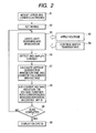
- FIG. 2 schematically shows a flow chart of the inspection method.
- the wafer 2 is set on the sample stage 21 to mount the upper and lower electrodes 6 and 7 to the wafer 2 (Step S51).
- Figs. 3A and 3B show the state in which the upper and lower electrodes 6 and 7 are mounted to the wafer 2.
- Fig. 3A shows the wafer 2 viewed from the upper surface side
- Fig. 3B show the wafer 2 viewed from the lower surface side.
- the wafer 2 is set on the sample stage 21 so that the surface on which the many laser diode chips 1 are stacked becomes the surface irradiated with the laser light, i.e. the upper surface.
- Fig. 3A the wafer 2 is set on the sample stage 21 so that the surface on which the many laser diode chips 1 are stacked becomes the surface irradiated with the laser light, i.e. the upper surface.
- the lower electrode 7 since the lower electrode 7 is attached on the side of the sample stage 21, a lead-out portion 5 is provided in order to perform the wiring for current detection.
- the upper and lower electrodes 6 and 7 are mounted to regions where the laser diode chips 1 are not formed in the wafer 2.
- dimensions and positions of the upper and lower electrodes 6 and 7 are not limited to the mode shown in Figs. 3A and 3B, and the dimensions and the positions can be freely set within the range where the irradiation to the laser diode chips 1 is not prevented.
- the anode 9a is connected to the upper electrode 6 mounted to the wafer 2 and the cathode 9b is connected to the lead-out portion 5.
- the anode 9a and the cathode 9b are connected to the current change detection and amplification unit 23 (Step S52).
- Step S53 In order to increase the detection sensitivity of the abnormal part, it is effective that a reverse bias or a forward bias is applied to the wafer 2, so that the voltage is applied to the wafer 2 from the voltage supplying unit 22 (Step S53). Similarly, in order to increase the detection sensitivity of the abnormal part, the temperature of the wafer 2 is controlled by the temperature control unit 24 (Step S54). Because the thermo-electromotive force current depends on the temperature of the sample, the temperature control unit 24 controls the temperature of the wafer 2 so that generation efficiency of the thermo-electromotive force current is maximized, which allows higher-reliability inspection to be performed.
- the laser light generation and scanning unit 11 scans on the wafer 2, the laser light generation and scanning unit 11 sequentially irradiates the laser diode chips 1 with the laser light 13 (Step S55). At this point, the laser light generation and scanning unit 11 perform the scanning so as to irradiate the oscillator (not shown) inside the laser diode 1 with the laser light 13 in a direction orthogonal to a lengthwise direction of the oscillator.
- the laser light 13 has energy (longer wavelength) lower than a band gap of the wafer 2 which is of the observation subject and the laser light 13 has the energy (shorter wavelength) which is sufficiently transmitted through the wafer 2.
- thermo-electromotive force current is generated due to the Seebeck effect by the irradiation of the laser light 13.
- the Seebeck effect means a phenomenon in which electromotive force is generated to cause passage of the current when temperature difference exists between two contacts of a closed circuit formed by two kinds of metals.
- a point which differs from the peripheral parts in physical properties or composition due to the abnormality such as the crystal defect, differs from the peripheral parts in thermal conduction or thermo-electric capacity, so that electric resistance is increased or decreased, compared with the surroundings, and the difference appears in the thermo-electromotive force.
- the current is changed in the abnormal part.
- the generated currents are respectively sent to the current change detection and amplification unit 23 from the upper electrode 6 and the lower electrode 7 through the anode 9a and the cathode 9b, and the current change detection and amplification unit 23 properly amplifies the currents (Step S56).
- the amplified micro current is averaged by a residence time of the laser light 13 at each scanning point to be converted into the voltage (Step S57).
- the A/D conversion of the voltage is performed to be stored in a memory which is located in the control unit 31 and corresponds to the scanning position (Step S58). It is confirmed that the scanning of all the laser diode chips 1 on the wafer 2 is completed (Step S59), and the irradiation of the laser light 13 is ended.
- the control unit 31 converts the voltage value corresponding to each scanning point in the memory into a luminance signal and transmits the luminance signal with data of the scanning point to CRT 32.
- CRT 32 two-dimensionally displays the data on a screen (Step S60). Therefore, the change in contrast can be observed while corresponding to the change in current caused by the irradiation of the laser light scanning (presence or absence of the abnormal part).
- pseudo-color for example, 256-gray-scale display. It is possible that marking can be performed by ink or the like to the laser diode chip 1 in which the trouble is found. Therefore, it is possible that the defective laser diode chip 1 or the wafer 2 including the defective laser diode chip 1 is caused not to proceed to the next production process.
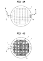
- the method for inspecting a semiconductor device chip wafer according to a second embodiment of the invention will be described below.
- the second embodiment differs from the first embodiment in that a single-chip electrode 18a is previously formed in the laser diode chip 1 formed on the wafer 2.
- Fig. 4A shows the wafer 2 viewed from the upper surface side
- Fig. 4B shows the wafer 2 viewed from the lower surface side.
- the upper electrode 6 is mounted to the surface of the wafer 2 in which the laser diode chip 1 is not formed, and the lower electrode 7 and the lead-out portion 5 are mounted to the surface of the wafer 2 in which the laser diode chip 1 is formed.
- the inspection method of the second embodiment it is possible that the single-chip electrode 18a is previously formed. Therefore, the inspection method of the second embodiment contributes to simplification of the manufacturing process.
- Fig. 5A shows the wafer 2 viewed,from the upper surface side
- Fig. 5B shows the wafer 2 viewed from the lower surface side.
- the surface in which the laser diode chip 1 is formed is set to the upper surface
- the surface in which the laser diode chip 1 is not formed is set to the lower surface.
- a single-chip electrode 18b is previously formed in the laser diode chip 1 on the upper surface of the wafer 2.
- an aperture 41 is provided in the single-chip electrode 18b.
- Another single-chip electrode 18c is formed on the surface of the wafer 2 in which the laser diode chip 1 is not formed.
- the aperture is not particularly formed in the single-chip electrode 18c, and the position and the shape of the single-chip 18c are formed such that the whole surface of the laser diode chip 1 is covered with the single-chip electrode 18c.
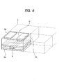
- Fig. 6 is an expanded view in which the laser diode chip 1 is cut out.
- the aperture 41 is located above oscillator 8, and the shape of the aperture 41 is formed so that the irradiation of the laser light 13 to the oscillator 8 is not interrupted.
- the upper electrode 6 is mounted onto the surface of the wafer 2 in which the laser diode chip 1 is formed, and the lower electrode 7 and the lead-out portion 5 are mounted onto the surface of the wafer 2 in which the laser diode chip 1 is not formed.
- the aperture through which the oscillator 8 can be irradiated with the laser light 13 is previously secured above the oscillator 8, which allows the same inspection as the first and second embodiments to be performed. Further, in the third embodiment, it is possible to complete up to the process in which the single-chip electrodes 18b and 18c are previously formed. Therefore, the third embodiment also contributes to the simplification of the manufacturing process.
- the method and apparatus for inspecting a semiconductor device chip wafer of the invention are not limited to the mode which utilizes the thermo-electromotive force generated by the irradiation of the laser light.
- the method in which the current is passed through the wafer 2 of the inspection subject and the wafer 2 is irradiated with the laser light 13 can be thought as an example.
- This method utilizes temperature dependence on resistance value as a principle of the defect detection. Namely, the temperature is increased in a part irradiated with the laser light 13 and the electric resistance is changed in the part in accordance with the increase in temperature.
- the wafer 2 has the crystal defect, the part in which the crystal defect is located differs from the normal part in the change in electric resistance.
- the thermal conductivity becomes worse and the difference between the defective part and the normal part is generated in the temperature rise or the change in electric resistance.
- the defect point can be specified on the basis of the above-described principle.
- the temperature of the wafer 2 is controlled by the temperature control unit 24.
- the invention is applied to the method of detecting the defect in a crystalline structure of the compound-semiconductor laser diode chip were described in the embodiments. However, the invention is not limited to the above-described embodiments, and the invention can be applied to other semiconductor devices. Further, the invention is effective when the inspection is performed by using the quantum beam such as an electron beam and an ion beam in addition to the laser light.
- the quantum beam such as an electron beam and an ion beam in addition to the laser light.
- a wafer is irradiated with laser light having a wavelength which is transmitted through an inside of a crystal of the wafer and does not generate electromotive force due to photo-excitation while the laser light is scanned.
- thermo-electromotive force is generated in a crystalline abnormal part of the wafer by Seebeck effect.
- a defect inside the crystal is detected such that the thermo-electromotive force is detected by a change in voltage or current which appears between an anode and a cathode of the wafer and the thermo-electromotive force is displayed on CRT.
Landscapes
- Engineering & Computer Science (AREA)
- Physics & Mathematics (AREA)
- Computer Hardware Design (AREA)
- Microelectronics & Electronic Packaging (AREA)
- Health & Medical Sciences (AREA)
- Computer Vision & Pattern Recognition (AREA)
- Electromagnetism (AREA)
- Toxicology (AREA)
- General Engineering & Computer Science (AREA)
- General Physics & Mathematics (AREA)
- Testing Or Measuring Of Semiconductors Or The Like (AREA)
- Semiconductor Lasers (AREA)
Abstract
Description
- The present invention relates to a method and an apparatus for observing, analyzing, and inspecting a crystal defect which are suitable for use in analysis and inspection of a crystal defect, a junction breakage caused by an electric stress, or the like inside a wafer in which semiconductor device chips, in particular, compound-semiconductor laser diode device chips are integrated.
- A typical compound-semiconductor laser diode device mainly includes the laser diode chips in which a stacked structure made of several kinds of semiconductors is formed. An oscillator (stripe) is provided in the laser diode chip. The oscillator confines laser light and amplifies the laser light by resonance. Many technologies have been developed for failure analysis and inspection of the compound-semiconductor laser diode (hereinafter referred to as laser diode).
- The inspection of the laser diode includes an electrical and optical characteristics measurement. A near field pattern (NFP) observation method is well known as the electrical and optical characteristics measurement. In the NFP observation method, a light-emission state in a laser-light emission position at an end face of the laser diode chip is two-dimensionally found with an infrared camera to observe a light-emission shape of the laser diode, and an abnormality is discriminated by comparing the laser diode of the inspection subject to the nondefective unit. The observation of the NFP observation method is performed in a manner that magnifies the light-emission position with an optical microscope while the laser diode chip is caused to emit the laser light, finds NFP of the light-emission position with the infrared camera, and displays NFP on a monitor screen (For example, see "Insight into Semiconductor Laser" 2nd edition, edited by Minoru KONUMA and Mitsuyoshi SHIBATA, Kougakutosho Ltd., May 25, 1998)).
- An aging method for screening a defective unit due to the crystal defect is also the well-known art. In the aging method, the defective unit is discriminated from a change in optical output after a predetermined time has elapsed.
- In the conventional method and apparatus for analyzing and inspecting a semiconductor laser diode device described above, there are the following problems.
- In the method for measuring an electrical and optical characteristics, although the defective unit which does not satisfy initially-required design specifications can be detected, the defective unit which is degraded with time by the crystal defect located inside the chip can not be detected. In the NFP observation method, because only the end face reflecting the laser light is observed, only a trace of a catastrophic optical damage (COD) which appears as optical information on the end face can detected, and it is difficult to check the abnormality such as the crystal defect located inside the chip.
- In the aging method, it is necessary to perform operation for all the finished units in a high temperature environment and it is also necessary to pay close attention to handling of the device or the apparatus so that the breakage of the device is not generated during the aging. Further, sometimes it takes several hours to tens of hours to perform the aging. Therefore, from a viewpoint of manufacturing cost, the aging method has the large problem. Particularly, the requirement of the aging for long hours becomes a large obstacle in mass production and reduction of the manufacturing cost can not be expected.
- Further, in these conventional inspection methods, basically it is necessary to perform the inspection in the state in which each chip is cut out from the wafer or in the state in which the device is almost finished. Therefore, it spends time to perform the inspection in the case of total inspection, and it is impossible to completely detect the defective unit in the case of sampling inspection. When the defective unit is detected, there is also the problem that the processes through which the defective unit is produced go to waste.
- In view of the foregoing, it is an object of the invention to provide the method and the apparatus which can simply and securely perform the observation and the detection of the abnormality such as the crystal defect and the breakage trace inside the semiconductor device such as the laser diode chip while the semiconductor device is in the wafer state.
- A method for inspecting a semiconductor device chip wafer of the invention includes a step of irradiating a wafer in which semiconductor device chips are integrated with a quantum beam having a wavelength which is transmitted through an inside of a crystal of the wafer and does not generate electromotive force due to excitation while the quantum beam is scanned, and a step of detecting the thermo-electromotive force generated in a crystalline abnormal part of the wafer by the irradiation by a change in voltage or current which appears between a surface of and a backside of the wafer and of displaying the thermo-electromotive force.
- An apparatus for inspecting a semiconductor device chip wafer of the invention includes irradiating means for irradiating a wafer in which semiconductor device chips are integrated with a quantum beam having a wavelength which is transmitted through an inside of a crystal of the wafer and does not generate electromotive force due to excitation while the quantum beam is scanned, and detecting and displaying means for detecting the thermo-electromotive force generated in a crystalline abnormal part of the wafer.by the irradiation by a change in voltage or current which appears between a surface of and a backside of the wafer and for displaying the thermo-electromotive force.
- When the defective point of the semiconductor device is irradiated with the quantum beam to heat the defective (abnormal) point, the thermal-electromotive force is generated by Seebeck effect and the current transiently passes through the wafer. The defect located in the oscillator and a peripheral area of the oscillator in the semiconductor device can be easily detected with high reliability by detecting intensity of the current.
- When the change in voltage or current is detected, a forward bias or a reverse bias can be applied between an anode and a cathode of the wafer. Therefore, detection sensitivity of the abnormal part can be increased and the reliability of the inspection can be improved.
- When the change in voltage or current is detected, a temperature of the wafer is controlled to the temperature in which the generation of the current is substantially maximized. Therefore, the detection sensitivity of the abnormal part can be increased and the reliability of the inspection can be improved.
- The inspection result can be visualized by displaying a relationship between an irradiation position of the laser light and the change in voltage or current corresponding to the irradiation position in a form of a display image. Therefore, the defect position can be visually directly comprehended and user-friendliness and reliability of the inspection can be improved.
- A single-chip electrode of each laser diode chip is previously provided in only one of the surface of and the backside of the semiconductor laser diode wafer, and the irradiation can be performed from the surface in which the single-chip electrode is not provided. Alternatively, a single-chip electrode having an aperture along an oscillator of each laser diode chip is previously provided in at least one of the surface of and the backside of the wafer, and the irradiation can be performed through the aperture. Therefore, the single-chip electrode finally required in the semiconductor laser diode can be previously mounted, and the method contributes to simplification of the manufacturing process.
- It is also possible that the wafer is previously divided into a plurality of pieces to perform the inspection in each of the divided wafers. Therefore, even when there is a limitation of a size of the inspection apparatus, the invention can be effectively realized.
- Other features and advantages of the present invention will be apparent from the following description taken in conjunction with the accompanying drawings, in which like reference characters designate the same or similar parts throughout the figures thereof
- The accompanying drawings, which are incorporated in and constitute a part of the specification, illustrate embodiments of the invention and, together with the description, serve to explain the principles of the invention.
- Fig. 1 is an overall view showing a configuration of an apparatus for inspecting a semiconductor device chip wafer of the invention;
- Fig. 2 is a flow chart of a method for a semiconductor of the invention;
- Figs. 3A and 3B are explanatory views of an electrode mounting method according to a first embodiment of the invention;
- Figs. 4A and 4B are explanatory views of the electrode mounting method according to a second embodiment of the invention;
- Figs. 5A and 5B are explanatory views of the electrode mounting method according to a third embodiment of the invention; and
- Fig. 6 is an outline view of a laser diode chip according to the third embodiment of the invention.
-
- The accompanying drawings, which are incorporated in and constitute a part of the specification, illustrate embodiments of the invention and, together with the description, serve to explain the principles of the invention.
- Preferred embodiments of the invention will be described below referring to the accompanying drawings. Fig. 1 is an overall view showing a configuration of the apparatus for inspecting a semiconductor device chip wafer according to an embodiment of the invention.
- A
sample stage 21 is one on which the semiconductor device chip wafer (hereinafter referred to as wafer 2) which is of a sample is set. Thewafer 2 in which the compound-semiconductor laser diode chips (hereinafter referred to as laser diode chips 1) are integrated is set on and fixed to thesample stage 21. The whole of thewafer 2 can become a single inspection subject. In view of the limitation of the inspection apparatus, it is also possible to previously divide thewafer 2 into the proper number of pieces having a proper size, for example, by the method of cutting out thewafer 2 in strips in each line oflaser diode chip 1. - An
upper electrode 6 and alower electrode 7 are mounted on an upper surface and a lower surface of thewafer 2 respectively. Theupper electrode 6 and thelower electrode 7 are connected to ananode 9a and acathode 9b respectively. Each one end of theanode 9a andcathode 9b is connected to a current change detection andamplification unit 23. The current change detection andamplification unit 23 detects and amplifies the change in current generated inside the wafer at the instance of the irradiation of each point in thewafer 2 withlaser light 13. - The
sample stage 21 is connected to avoltage supplying unit 22 which supplies voltage to thewafer 2. Thesample stage 21 is also connected to atemperature control unit 24 through aheating medium pipe 25. Thetemperature control unit 24 controls a temperature of thewafer 2. - A laser light generation and
scanning unit 11 is provided in an upper portion of thesample stage 21. The laser light generation andscanning unit 11 generates thelaser light 13 and scans thelaser light 13 on thewafer 2. Amicroscope 12 for focusing a light flux of thelaser light 13 is provided between the laser light generation andscanning unit 11 and thesample stage 21. The laser light generation andscanning unit 11 and themicroscope 12 can vertically observe the peripheral portion of the oscillator (not shown) located in eachlaser diode chip 1 of thewafer 2 in order from a top surface. - A
control unit 31 is connected to the laser light generation andscanning unit 11, the current change detection andamplification unit 23, andtemperature control unit 24. Thecontrol unit 31 receives pieces of information such as a scanning position of thelaser light 13, the change in current of thewafer 2, the temperature of thewafer 2, and the voltage applied to thewafer 2 and performs processing of the pieces of information to store the pieces of information. Thecontrol unit 31 is also connected toCRT 32 which converts an observation result into positional information and luminance information to perform display, and thecontrol unit 31 transmits the processed and stored result toCRT 32 if necessary. - Then, the method of inspecting the
wafer 2 according to the embodiment will be described. Fig. 2 schematically shows a flow chart of the inspection method. - The
wafer 2 is set on thesample stage 21 to mount the upper andlower electrodes lower electrodes wafer 2. Fig. 3A shows thewafer 2 viewed from the upper surface side and Fig. 3B show thewafer 2 viewed from the lower surface side. As shown in Fig. 3A, thewafer 2 is set on thesample stage 21 so that the surface on which the manylaser diode chips 1 are stacked becomes the surface irradiated with the laser light, i.e. the upper surface. As shown in Fig. 3B, since thelower electrode 7 is attached on the side of thesample stage 21, a lead-outportion 5 is provided in order to perform the wiring for current detection. The upper andlower electrodes laser diode chips 1 are not formed in thewafer 2. However, dimensions and positions of the upper andlower electrodes laser diode chips 1 is not prevented. - Then, the
anode 9a is connected to theupper electrode 6 mounted to thewafer 2 and thecathode 9b is connected to the lead-outportion 5. Theanode 9a and thecathode 9b are connected to the current change detection and amplification unit 23 (Step S52). - In order to increase the detection sensitivity of the abnormal part, it is effective that a reverse bias or a forward bias is applied to the
wafer 2, so that the voltage is applied to thewafer 2 from the voltage supplying unit 22 (Step S53). Similarly, in order to increase the detection sensitivity of the abnormal part, the temperature of thewafer 2 is controlled by the temperature control unit 24 (Step S54). Because the thermo-electromotive force current depends on the temperature of the sample, thetemperature control unit 24 controls the temperature of thewafer 2 so that generation efficiency of the thermo-electromotive force current is maximized, which allows higher-reliability inspection to be performed. - While the laser light generation and
scanning unit 11 scans on thewafer 2, the laser light generation andscanning unit 11 sequentially irradiates thelaser diode chips 1 with the laser light 13 (Step S55). At this point, the laser light generation andscanning unit 11 perform the scanning so as to irradiate the oscillator (not shown) inside thelaser diode 1 with thelaser light 13 in a direction orthogonal to a lengthwise direction of the oscillator. In order to suppress the generation of optical beam induced current (OBIC) which is of the photo-excited current as much as possible, thelaser light 13 has energy (longer wavelength) lower than a band gap of thewafer 2 which is of the observation subject and thelaser light 13 has the energy (shorter wavelength) which is sufficiently transmitted through thewafer 2. - When the
wafer 2 has the abnormal part such as the crystal defect, the thermo-electromotive force current is generated due to the Seebeck effect by the irradiation of thelaser light 13. The Seebeck effect means a phenomenon in which electromotive force is generated to cause passage of the current when temperature difference exists between two contacts of a closed circuit formed by two kinds of metals. A point, which differs from the peripheral parts in physical properties or composition due to the abnormality such as the crystal defect, differs from the peripheral parts in thermal conduction or thermo-electric capacity, so that electric resistance is increased or decreased, compared with the surroundings, and the difference appears in the thermo-electromotive force. As a result, compared with the normal part, the current is changed in the abnormal part. The generated currents are respectively sent to the current change detection andamplification unit 23 from theupper electrode 6 and thelower electrode 7 through theanode 9a and thecathode 9b, and the current change detection andamplification unit 23 properly amplifies the currents (Step S56). The amplified micro current is averaged by a residence time of thelaser light 13 at each scanning point to be converted into the voltage (Step S57). Then, the A/D conversion of the voltage is performed to be stored in a memory which is located in thecontrol unit 31 and corresponds to the scanning position (Step S58). It is confirmed that the scanning of all thelaser diode chips 1 on thewafer 2 is completed (Step S59), and the irradiation of thelaser light 13 is ended. - Instead of the measurement of the current between the
anode 9a and thecathode 9b, it is also possible to directly measure the voltage between theanode 9a and thecathode 9b. - The
control unit 31 converts the voltage value corresponding to each scanning point in the memory into a luminance signal and transmits the luminance signal with data of the scanning point toCRT 32.CRT 32 two-dimensionally displays the data on a screen (Step S60). Therefore, the change in contrast can be observed while corresponding to the change in current caused by the irradiation of the laser light scanning (presence or absence of the abnormal part). In addition to the luminance signal, it is also possible to use pseudo-color (for example, 256-gray-scale display). It is possible that marking can be performed by ink or the like to thelaser diode chip 1 in which the trouble is found. Therefore, it is possible that the defectivelaser diode chip 1 or thewafer 2 including the defectivelaser diode chip 1 is caused not to proceed to the next production process. - The method for inspecting a semiconductor device chip wafer according to a second embodiment of the invention will be described below. The second embodiment differs from the first embodiment in that a single-chip electrode 18a is previously formed in the
laser diode chip 1 formed on thewafer 2. Fig. 4A shows thewafer 2 viewed from the upper surface side and Fig. 4B shows thewafer 2 viewed from the lower surface side. When the single-chip electrode 18a is formed, since the irradiation of thelaser light 13 is interrupted by the single-chip electrode 18a and the effective inspection becomes difficult, thewafer 2 is set on thesample stage 21 so that the surface on which the single-chip electrode 18a is formed becomes the backside with respect to the irradiation direction of thelaser light 13. As a result, theupper electrode 6 is mounted to the surface of thewafer 2 in which thelaser diode chip 1 is not formed, and thelower electrode 7 and the lead-outportion 5 are mounted to the surface of thewafer 2 in which thelaser diode chip 1 is formed. In the inspection method of the second embodiment, it is possible that the single-chip electrode 18a is previously formed. Therefore, the inspection method of the second embodiment contributes to simplification of the manufacturing process. - Then, The method for inspecting a semiconductor device chip wafer according to a third embodiment of the invention will be described. Fig. 5A shows the
wafer 2 viewed,from the upper surface side and Fig. 5B shows thewafer 2 viewed from the lower surface side. In the third embodiment, similarly to the first embodiment, the surface in which thelaser diode chip 1 is formed is set to the upper surface, and the surface in which thelaser diode chip 1 is not formed is set to the lower surface. A single-chip electrode 18b is previously formed in thelaser diode chip 1 on the upper surface of thewafer 2. However, unlike the second embodiment, anaperture 41 is provided in the single-chip electrode 18b. Another single-chip electrode 18c is formed on the surface of thewafer 2 in which thelaser diode chip 1 is not formed. The aperture is not particularly formed in the single-chip electrode 18c, and the position and the shape of the single-chip 18c are formed such that the whole surface of thelaser diode chip 1 is covered with the single-chip electrode 18c. Fig. 6 is an expanded view in which thelaser diode chip 1 is cut out. Theaperture 41 is located aboveoscillator 8, and the shape of theaperture 41 is formed so that the irradiation of thelaser light 13 to theoscillator 8 is not interrupted. Theupper electrode 6 is mounted onto the surface of thewafer 2 in which thelaser diode chip 1 is formed, and thelower electrode 7 and the lead-outportion 5 are mounted onto the surface of thewafer 2 in which thelaser diode chip 1 is not formed. The aperture through which theoscillator 8 can be irradiated with thelaser light 13 is previously secured above theoscillator 8, which allows the same inspection as the first and second embodiments to be performed. Further, in the third embodiment, it is possible to complete up to the process in which the single-chip electrodes - Although the preferred embodiments were described above, the method and apparatus for inspecting a semiconductor device chip wafer of the invention are not limited to the mode which utilizes the thermo-electromotive force generated by the irradiation of the laser light. The method in which the current is passed through the
wafer 2 of the inspection subject and thewafer 2 is irradiated with thelaser light 13 can be thought as an example.
This method utilizes temperature dependence on resistance value as a principle of the defect detection. Namely, the temperature is increased in a part irradiated with thelaser light 13 and the electric resistance is changed in the part in accordance with the increase in temperature. However, when thewafer 2 has the crystal defect, the part in which the crystal defect is located differs from the normal part in the change in electric resistance. For example, when thewafer 2 has the defect such as a void, the thermal conductivity becomes worse and the difference between the defective part and the normal part is generated in the temperature rise or the change in electric resistance. The defect point can be specified on the basis of the above-described principle. In this case, in order to increase the detection sensitivity, and in order to decrease the amount of current in the state in which thewafer 2 is not irradiated with thelaser light 13, it is also effective that the temperature of thewafer 2 is controlled by thetemperature control unit 24. - The cases in which the invention is applied to the method of detecting the defect in a crystalline structure of the compound-semiconductor laser diode chip were described in the embodiments. However, the invention is not limited to the above-described embodiments, and the invention can be applied to other semiconductor devices. Further, the invention is effective when the inspection is performed by using the quantum beam such as an electron beam and an ion beam in addition to the laser light.
- A wafer is irradiated with laser light having a wavelength which is transmitted through an inside of a crystal of the wafer and does not generate electromotive force due to photo-excitation while the laser light is scanned. When a temperature of the wafer is increased by the irradiation, thermo-electromotive force is generated in a crystalline abnormal part of the wafer by Seebeck effect. A defect inside the crystal is detected such that the thermo-electromotive force is detected by a change in voltage or current which appears between an anode and a cathode of the wafer and the thermo-electromotive force is displayed on CRT.
Claims (13)
- A method for inspecting a semiconductor device chip wafer comprising:an irradiating step of irradiating a wafer in which semiconductor device chips are integrated with a quantum beam having a wavelength which is transmitted through an inside of a crystal of the wafer and does not generate electromotive force due to excitation while the quantum beam is scanned; anda detection and display step of detecting the thermo-electromotive force generated in a crystalline abnormal part of the wafer by the irradiation by a change in voltage or current which appears between a surface of and a backside of the wafer, and of displaying the thermo-electromotive force.
- The inspection method according to claim 1, wherein a forward bias or a reverse bias is applied between the surface of and the backside of the wafer when the change in voltage or current is detected.
- The inspection method according to claim 1, wherein a temperature of the wafer is controlled to the temperature in which the generation of the current is substantially maximized when the change in voltage or current is detected.
- A method for inspecting a semiconductor device chip wafer comprising:a step of passing constant current between a surface of and a backside of a wafer in which semiconductor device chips are integrated;a step of irradiating the wafer with a quantum beam having a wavelength which is transmitted through an inside of a crystal of the wafer and does not generate electromotive force due to excitation while the quantum beam is scanned; anda step of detecting a change in current generated by irradiating a crystalline abnormal part of the wafer and of displaying the change in current.
- The inspection method according to claim 4, wherein the display is performed by displaying a relationship between an irradiation position of the quantum beam and the change in voltage or current corresponding to the irradiation position in a form of a display image.
- The inspection method according to claim 5, further comprising a step of previously providing a single-chip electrode of each laser diode chip in only one of the surface of and the backside of the wafer, wherein the semiconductor device is a semiconductor laser diode, and the irradiation is performed from the surface in which the single-chip electrode is not provided.
- The inspection method according to claim 5, wherein further comprising a step of previously providing a single-chip electrode having an aperture along an oscillator of each laser diode chip in at least one of the surface of and the backside of the wafer, wherein the semiconductor device is a semiconductor laser diode having the oscillator, and the irradiation is performed through the aperture.
- The inspection method according to claim 5, further comprising a step of previously dividing the wafer into a plurality of pieces, wherein the irradiating step and the detecting and displaying step are performed in each of the divided wafers.
- An apparatus for inspecting a semiconductor device chip wafer comprising:irradiating means for irradiating a wafer in which semiconductor device chips are integrated with a quantum beam having a wavelength which is transmitted through an inside of a crystal of the wafer and does not generate electromotive force due to excitation while the quantum beam is scanned; anddetecting and displaying means for detecting the thermo-electromotive force generated in a crystalline abnormal part of the wafer by the irradiation by a change in voltage or current which appears between a surface of and a backside of the wafer, and for displaying the thermo-electromotive force.
- The inspection apparatus according to claim 9, further comprising means for applying a forward bias or a reverse bias between the surface of and the backside of the wafer when the change in voltage or current is detected.
- The inspection apparatus according to claim 9, further comprising means for controlling a temperature of the wafer to the temperature in which the generation of the current is substantially maximized when the change in voltage or current is detected.
- An apparatus for inspecting a semiconductor device chip wafer comprising:irradiating means for irradiating a wafer in which semiconductor device chips are integrated with a quantum beam having a wavelength which is transmitted through an inside of a crystal of the wafer and does not generate electromotive force due to excitation at the same time when constant current is passed between a surface of and a backside of the wafer while the quantum beam is scanned; anddisplaying means for detecting a change in current generated by irradiating a crystalline abnormal part of the wafer and of displaying the change in current.
- The inspection apparatus according to claim 12, wherein the displaying means is the means for displaying a relationship between an irradiation position of the quantum beam and the change in voltage or current corresponding to the irradiation position in a form of a display image.
Applications Claiming Priority (2)
| Application Number | Priority Date | Filing Date | Title |
|---|---|---|---|
| JP2003274511A JP4136832B2 (en) | 2003-07-15 | 2003-07-15 | Inspection method and inspection apparatus for semiconductor laser diode chip |
| JP2003274511 | 2003-07-15 |
Publications (2)
| Publication Number | Publication Date |
|---|---|
| EP1498727A1 true EP1498727A1 (en) | 2005-01-19 |
| EP1498727B1 EP1498727B1 (en) | 2009-04-15 |
Family
ID=33475552
Family Applications (1)
| Application Number | Title | Priority Date | Filing Date |
|---|---|---|---|
| EP04015767A Expired - Lifetime EP1498727B1 (en) | 2003-07-15 | 2004-07-05 | Method for inspecting semiconductor device |
Country Status (6)
| Country | Link |
|---|---|
| US (2) | US7015051B2 (en) |
| EP (1) | EP1498727B1 (en) |
| JP (1) | JP4136832B2 (en) |
| KR (1) | KR100633460B1 (en) |
| DE (1) | DE602004020550D1 (en) |
| TW (1) | TWI245356B (en) |
Cited By (2)
| Publication number | Priority date | Publication date | Assignee | Title |
|---|---|---|---|---|
| EP2009455A1 (en) | 2007-06-29 | 2008-12-31 | NEC Electronics Corporation | Failure analysis method and failure analysis apparatus |
| CN110031188A (en) * | 2019-03-29 | 2019-07-19 | 上海华岭集成电路技术股份有限公司 | Integrated circuit optical chip aperture test method |
Families Citing this family (15)
| Publication number | Priority date | Publication date | Assignee | Title |
|---|---|---|---|---|
| US6898138B2 (en) * | 2002-08-29 | 2005-05-24 | Micron Technology, Inc. | Method of reducing variable retention characteristics in DRAM cells |
| JP4334927B2 (en) * | 2003-06-27 | 2009-09-30 | キヤノン株式会社 | Inspection method and inspection apparatus for semiconductor laser diode chip |
| KR100688551B1 (en) | 2005-06-07 | 2007-03-02 | 삼성전자주식회사 | Semiconductor wafer marking device with interlock function and semiconductor wafer marking method using the same |
| JP4363368B2 (en) * | 2005-06-13 | 2009-11-11 | 住友電気工業株式会社 | Method for evaluating damage to compound semiconductor member, and method for producing compound semiconductor member |
| JP2007081197A (en) * | 2005-09-15 | 2007-03-29 | Sony Corp | Semiconductor laser and manufacturing method thereof |
| JP4694970B2 (en) * | 2006-01-16 | 2011-06-08 | 三洋電機株式会社 | Semiconductor element analysis method |
| FR2902926B1 (en) * | 2006-06-22 | 2008-10-24 | Commissariat Energie Atomique | METHOD AND DEVICE FOR MONITORING THERMAL PROCESSING OF A MICROTECHNOLOGICAL SUBSTRATE |
| KR100827819B1 (en) * | 2007-02-21 | 2008-05-07 | 전북대학교산학협력단 | Carrier type measuring system for semiconductor nanomaterials and carrier type measuring method for semiconductor nanomaterials |
| JP4374552B2 (en) * | 2007-04-12 | 2009-12-02 | ソニー株式会社 | Substrate manufacturing method, substrate manufacturing system, and display device manufacturing method |
| US7919973B2 (en) * | 2007-06-22 | 2011-04-05 | Microchip Technology Incorporated | Method and apparatus for monitoring via's in a semiconductor fab |
| JP6137536B2 (en) * | 2013-04-26 | 2017-05-31 | 日本電産リード株式会社 | Substrate inspection apparatus and substrate inspection method |
| DE102016008509A1 (en) * | 2016-07-13 | 2018-01-18 | Siltectra Gmbh | Laser conditioning of solids with prior knowledge from previous processing steps |
| JP7092089B2 (en) * | 2019-04-10 | 2022-06-28 | 株式会社Sumco | Conductive type discrimination device and conductive type discrimination method for semiconductor products |
| JP2022191643A (en) * | 2021-06-16 | 2022-12-28 | 住友電気工業株式会社 | Method for manufacturing surface emitting laser, method for inspecting surface emitting laser, and inspection apparatus for surface emitting laser |
| CN118518676A (en) * | 2024-07-09 | 2024-08-20 | 深圳市鹏乐智能系统有限公司 | LED chip defect detection method and system based on artificial intelligence |
Citations (4)
| Publication number | Priority date | Publication date | Assignee | Title |
|---|---|---|---|---|
| US5422498A (en) * | 1993-04-13 | 1995-06-06 | Nec Corporation | Apparatus for diagnosing interconnections of semiconductor integrated circuits |
| DE19725679A1 (en) * | 1997-06-18 | 1999-01-28 | Innomess Elektronik Gmbh | Detecting electrical inhomogeneities of semiconductors |
| US5952837A (en) | 1995-07-18 | 1999-09-14 | Mitsubishi Denki Kabushiki Kaisha | Scanning photoinduced current analyzer capable of detecting photoinduced current in nonbiased specimen |
| US20020106820A1 (en) | 1998-09-28 | 2002-08-08 | Nec Corporation | Device and method for nondestructive inspection on semiconductor device |
Family Cites Families (2)
| Publication number | Priority date | Publication date | Assignee | Title |
|---|---|---|---|---|
| US5708371A (en) * | 1995-03-16 | 1998-01-13 | Mitsubishi Denki Kabushiki Kaisha | Scanning photoinduced current analyzer capable of detecting photoinduced current in nonbiased specimen |
| JP4334927B2 (en) | 2003-06-27 | 2009-09-30 | キヤノン株式会社 | Inspection method and inspection apparatus for semiconductor laser diode chip |
-
2003
- 2003-07-15 JP JP2003274511A patent/JP4136832B2/en not_active Expired - Fee Related
-
2004
- 2004-06-25 TW TW093118671A patent/TWI245356B/en not_active IP Right Cessation
- 2004-06-30 US US10/879,060 patent/US7015051B2/en not_active Expired - Fee Related
- 2004-07-05 DE DE602004020550T patent/DE602004020550D1/en not_active Expired - Lifetime
- 2004-07-05 EP EP04015767A patent/EP1498727B1/en not_active Expired - Lifetime
- 2004-07-15 KR KR1020040054978A patent/KR100633460B1/en not_active Expired - Fee Related
-
2005
- 2005-11-28 US US11/287,458 patent/US7332362B2/en not_active Expired - Fee Related
Patent Citations (4)
| Publication number | Priority date | Publication date | Assignee | Title |
|---|---|---|---|---|
| US5422498A (en) * | 1993-04-13 | 1995-06-06 | Nec Corporation | Apparatus for diagnosing interconnections of semiconductor integrated circuits |
| US5952837A (en) | 1995-07-18 | 1999-09-14 | Mitsubishi Denki Kabushiki Kaisha | Scanning photoinduced current analyzer capable of detecting photoinduced current in nonbiased specimen |
| DE19725679A1 (en) * | 1997-06-18 | 1999-01-28 | Innomess Elektronik Gmbh | Detecting electrical inhomogeneities of semiconductors |
| US20020106820A1 (en) | 1998-09-28 | 2002-08-08 | Nec Corporation | Device and method for nondestructive inspection on semiconductor device |
Non-Patent Citations (2)
| Title |
|---|
| "Insight into Semiconductor Laser", 25 May 1998, KOUGAKUTOSHO LTD. |
| SCHURIG T ET AL: "NONDESTRUCTIVE WAFER INSPECTION ULTILIZING SQUIDS", INSTITUTE OF PHYSICS CONFERENCE SERIES, IOP PUBLISHING,, GB, no. 160, 7 September 1997 (1997-09-07), pages 149 - 152, XP001006353, ISSN: 0951-3248 * |
Cited By (3)
| Publication number | Priority date | Publication date | Assignee | Title |
|---|---|---|---|---|
| EP2009455A1 (en) | 2007-06-29 | 2008-12-31 | NEC Electronics Corporation | Failure analysis method and failure analysis apparatus |
| US7825673B2 (en) | 2007-06-29 | 2010-11-02 | Nec Electronics Corporation | Failure analysis method and failure analysis apparatus |
| CN110031188A (en) * | 2019-03-29 | 2019-07-19 | 上海华岭集成电路技术股份有限公司 | Integrated circuit optical chip aperture test method |
Also Published As
| Publication number | Publication date |
|---|---|
| KR20050008530A (en) | 2005-01-21 |
| US7015051B2 (en) | 2006-03-21 |
| US20050012923A1 (en) | 2005-01-20 |
| US20060079058A1 (en) | 2006-04-13 |
| KR100633460B1 (en) | 2006-10-16 |
| TW200504910A (en) | 2005-02-01 |
| TWI245356B (en) | 2005-12-11 |
| JP4136832B2 (en) | 2008-08-20 |
| EP1498727B1 (en) | 2009-04-15 |
| DE602004020550D1 (en) | 2009-05-28 |
| US7332362B2 (en) | 2008-02-19 |
| JP2005039054A (en) | 2005-02-10 |
Similar Documents
| Publication | Publication Date | Title |
|---|---|---|
| US7015051B2 (en) | Method for inspecting semiconductor device | |
| US7385686B2 (en) | Method and apparatus for inspecting semiconductor device | |
| JP6131250B2 (en) | Method and apparatus for inspection of light emitting semiconductor devices using photoluminescence imaging | |
| JP4248249B2 (en) | Detection and classification of semiconductor microdefects | |
| CN101354366B (en) | Failure analysis method and failure analysis apparatus | |
| JP3917154B2 (en) | Defect evaluation method and apparatus for semiconductor sample | |
| US9222970B2 (en) | Fault position analysis method and fault position analysis device for semiconductor device | |
| JPH0750331A (en) | Evaluation apparatus and method for semiconductor light emitting device | |
| EP3654046A1 (en) | Non-destructive inspection system for detecting defects in compound semiconductor wafer and method of operating the same | |
| US6980010B2 (en) | Method and apparatus for inspecting wire breaking of integrated circuit | |
| JP2518533B2 (en) | Inspection device for internal interconnection of semiconductor integrated circuits | |
| JP2000208577A (en) | Semiconductor evaluating method and defect position specifying device | |
| KR102170357B1 (en) | Method for non-destructive defect detection | |
| US7466404B1 (en) | Technique for diagnosing and screening optical interconnect light sources | |
| JPH08274138A (en) | Method and apparatus for detecting defects in insulating film of semiconductor device | |
| CN121639564A (en) | Semiconductor laser chip defect identification method, device, equipment and medium | |
| KR20220078146A (en) | Nondestructive assessment system for micro led chip | |
| Barton | Optoelectronic Device Failure Analysis | |
| Gallant et al. | High-power diode array reliability experiment | |
| Miller et al. | Electron Beam Induced Luminescence | |
| JP2009170757A (en) | Optical semiconductor device inspection method | |
| JPH11317430A (en) | Inspection method for semiconductor device | |
| JPH05175293A (en) | Semiconductor chip analysis method | |
| KR20150081613A (en) | System for inspecting the defect of solar battery and Method therefor | |
| JP2013004567A (en) | Inspection apparatus and method |
Legal Events
| Date | Code | Title | Description |
|---|---|---|---|
| PUAI | Public reference made under article 153(3) epc to a published international application that has entered the european phase |
Free format text: ORIGINAL CODE: 0009012 |
|
| AK | Designated contracting states |
Kind code of ref document: A1 Designated state(s): AT BE BG CH CY CZ DE DK EE ES FI FR GB GR HU IE IT LI LU MC NL PL PT RO SE SI SK TR |
|
| AX | Request for extension of the european patent |
Extension state: AL HR LT LV MK |
|
| 17P | Request for examination filed |
Effective date: 20050718 |
|
| AKX | Designation fees paid |
Designated state(s): DE FR GB |
|
| 17Q | First examination report despatched |
Effective date: 20070202 |
|
| GRAP | Despatch of communication of intention to grant a patent |
Free format text: ORIGINAL CODE: EPIDOSNIGR1 |
|
| GRAS | Grant fee paid |
Free format text: ORIGINAL CODE: EPIDOSNIGR3 |
|
| GRAA | (expected) grant |
Free format text: ORIGINAL CODE: 0009210 |
|
| AK | Designated contracting states |
Kind code of ref document: B1 Designated state(s): DE FR GB |
|
| REG | Reference to a national code |
Ref country code: GB Ref legal event code: FG4D |
|
| REF | Corresponds to: |
Ref document number: 602004020550 Country of ref document: DE Date of ref document: 20090528 Kind code of ref document: P |
|
| PLBE | No opposition filed within time limit |
Free format text: ORIGINAL CODE: 0009261 |
|
| STAA | Information on the status of an ep patent application or granted ep patent |
Free format text: STATUS: NO OPPOSITION FILED WITHIN TIME LIMIT |
|
| 26N | No opposition filed |
Effective date: 20100118 |
|
| PGFP | Annual fee paid to national office [announced via postgrant information from national office to epo] |
Ref country code: GB Payment date: 20120730 Year of fee payment: 9 |
|
| PGFP | Annual fee paid to national office [announced via postgrant information from national office to epo] |
Ref country code: FR Payment date: 20120808 Year of fee payment: 9 Ref country code: DE Payment date: 20120731 Year of fee payment: 9 |
|
| GBPC | Gb: european patent ceased through non-payment of renewal fee |
Effective date: 20130705 |
|
| REG | Reference to a national code |
Ref country code: FR Ref legal event code: ST Effective date: 20140331 |
|
| PG25 | Lapsed in a contracting state [announced via postgrant information from national office to epo] |
Ref country code: DE Free format text: LAPSE BECAUSE OF NON-PAYMENT OF DUE FEES Effective date: 20140201 Ref country code: GB Free format text: LAPSE BECAUSE OF NON-PAYMENT OF DUE FEES Effective date: 20130705 |
|
| REG | Reference to a national code |
Ref country code: DE Ref legal event code: R119 Ref document number: 602004020550 Country of ref document: DE Effective date: 20140201 |
|
| PG25 | Lapsed in a contracting state [announced via postgrant information from national office to epo] |
Ref country code: FR Free format text: LAPSE BECAUSE OF NON-PAYMENT OF DUE FEES Effective date: 20130731 |