EP1498517A1 - Method for producing silicon single crystal and, silicon single crystal and silicon wafer - Google Patents
Method for producing silicon single crystal and, silicon single crystal and silicon wafer Download PDFInfo
- Publication number
- EP1498517A1 EP1498517A1 EP03719172A EP03719172A EP1498517A1 EP 1498517 A1 EP1498517 A1 EP 1498517A1 EP 03719172 A EP03719172 A EP 03719172A EP 03719172 A EP03719172 A EP 03719172A EP 1498517 A1 EP1498517 A1 EP 1498517A1
- Authority
- EP
- European Patent Office
- Prior art keywords
- crystal
- silicon
- single crystal
- seed crystal
- silicon melt
- Prior art date
- Legal status (The legal status is an assumption and is not a legal conclusion. Google has not performed a legal analysis and makes no representation as to the accuracy of the status listed.)
- Granted
Links
Images

Classifications
-
- C—CHEMISTRY; METALLURGY
- C30—CRYSTAL GROWTH
- C30B—SINGLE-CRYSTAL GROWTH; UNIDIRECTIONAL SOLIDIFICATION OF EUTECTIC MATERIAL OR UNIDIRECTIONAL DEMIXING OF EUTECTOID MATERIAL; REFINING BY ZONE-MELTING OF MATERIAL; PRODUCTION OF A HOMOGENEOUS POLYCRYSTALLINE MATERIAL WITH DEFINED STRUCTURE; SINGLE CRYSTALS OR HOMOGENEOUS POLYCRYSTALLINE MATERIAL WITH DEFINED STRUCTURE; AFTER-TREATMENT OF SINGLE CRYSTALS OR A HOMOGENEOUS POLYCRYSTALLINE MATERIAL WITH DEFINED STRUCTURE; APPARATUS THEREFOR
- C30B29/00—Single crystals or homogeneous polycrystalline material with defined structure characterised by the material or by their shape
- C30B29/02—Elements
- C30B29/06—Silicon
-
- C—CHEMISTRY; METALLURGY
- C30—CRYSTAL GROWTH
- C30B—SINGLE-CRYSTAL GROWTH; UNIDIRECTIONAL SOLIDIFICATION OF EUTECTIC MATERIAL OR UNIDIRECTIONAL DEMIXING OF EUTECTOID MATERIAL; REFINING BY ZONE-MELTING OF MATERIAL; PRODUCTION OF A HOMOGENEOUS POLYCRYSTALLINE MATERIAL WITH DEFINED STRUCTURE; SINGLE CRYSTALS OR HOMOGENEOUS POLYCRYSTALLINE MATERIAL WITH DEFINED STRUCTURE; AFTER-TREATMENT OF SINGLE CRYSTALS OR A HOMOGENEOUS POLYCRYSTALLINE MATERIAL WITH DEFINED STRUCTURE; APPARATUS THEREFOR
- C30B15/00—Single-crystal growth by pulling from a melt, e.g. Czochralski method
- C30B15/20—Controlling or regulating
- C30B15/22—Stabilisation or shape controlling of the molten zone near the pulled crystal; Controlling the section of the crystal
-
- C—CHEMISTRY; METALLURGY
- C30—CRYSTAL GROWTH
- C30B—SINGLE-CRYSTAL GROWTH; UNIDIRECTIONAL SOLIDIFICATION OF EUTECTIC MATERIAL OR UNIDIRECTIONAL DEMIXING OF EUTECTOID MATERIAL; REFINING BY ZONE-MELTING OF MATERIAL; PRODUCTION OF A HOMOGENEOUS POLYCRYSTALLINE MATERIAL WITH DEFINED STRUCTURE; SINGLE CRYSTALS OR HOMOGENEOUS POLYCRYSTALLINE MATERIAL WITH DEFINED STRUCTURE; AFTER-TREATMENT OF SINGLE CRYSTALS OR A HOMOGENEOUS POLYCRYSTALLINE MATERIAL WITH DEFINED STRUCTURE; APPARATUS THEREFOR
- C30B15/00—Single-crystal growth by pulling from a melt, e.g. Czochralski method
- C30B15/36—Single-crystal growth by pulling from a melt, e.g. Czochralski method characterised by the seed, e.g. its crystallographic orientation
-
- Y—GENERAL TAGGING OF NEW TECHNOLOGICAL DEVELOPMENTS; GENERAL TAGGING OF CROSS-SECTIONAL TECHNOLOGIES SPANNING OVER SEVERAL SECTIONS OF THE IPC; TECHNICAL SUBJECTS COVERED BY FORMER USPC CROSS-REFERENCE ART COLLECTIONS [XRACs] AND DIGESTS
- Y10—TECHNICAL SUBJECTS COVERED BY FORMER USPC
- Y10T—TECHNICAL SUBJECTS COVERED BY FORMER US CLASSIFICATION
- Y10T117/00—Single-crystal, oriented-crystal, and epitaxy growth processes; non-coating apparatus therefor
- Y10T117/10—Apparatus
- Y10T117/1024—Apparatus for crystallization from liquid or supercritical state
- Y10T117/1032—Seed pulling
Definitions
- the present invention relates to a method of manufacturing a silicon single crystal using Czochralski method (hereinafter, occasionally referred to as "CZ method"), more particularly, a method of manufacturing a silicon single crystal grown by Chochralski method by use of a seed crystal having a tip end with a sharp-pointed shape or a truncation thereof without using Dash Necking method, and a silicon single crystal and a silicon wafer manufactured thereby.
- CZ method Czochralski method
- a silicon wafer which is obtained by processing a silicon single crystal grown by mainly CZ method into wafers, is used as a wafer for a substrate material on which a semiconductor device is formed.
- a silicon single crystal using CZ method generally a seed crystal having a shape shown in Fig. 2(A) or 2(B) is gently brought into contact with a silicon melt heated to 1420 °C of a melting point or more, and then the seed crystal is gradually pulled upward from the melt when a temperature of the seed crystal becomes steady. Thereby, a silicon single crystal is grown below the seed crystal.
- a necking portion where a diameter of the crystal grown following the seed crystal is once gradually lessened to about 3 - 5 mm is formed as shown in Fig. 4 in order to eliminate the slip dislocations.
- a diameter of the crystal is gently enlarged to a desired diameter (formation of an enlarging diameter portion), and then an approximately cylindrical silicon single crystal having a diameter required in a constant diameter portion thereof is pulled.
- Dash Necking method is a manufacturing method widely utilized when growing a silicon single crystal by CZ method.
- a silicon single crystal free from dislocation can be grown without lessening a diameter of the crystal to be grown at the tip end of the seed crystal to 5 mm or less. Therefore, it has an advantage in growing a crystal having a large diameter or a heavy crystal.
- slip dislocations are introduced into the seed crystal if the temperature of a silicon melt largely changes even while the tip end of the seed crystal is dipped into the silicon melt to the desired diameter and so on.
- a silicon wafer having a plane orientation of (100) or (111) in a main surface on which a semiconductor device is to be formed has been mainly utilized in view of physical characteristics and advantages in the processes of growing a crystal and fabricating a semiconductor device.
- transport of carriers when forming a semiconductor device considerably depends on a crystal orientation, in recent years, with the aim of enhancing the working speed of the semiconductor device, a silicon wafer having a plane orientation of (110) in which high switching speed is expected starts to attract attention (Nikkei Microdevices, the February 2001, No. 188, Nikkei BP Inc., published on February 1, 2001).
- the silicon wafer having a plane orientation of (110) it is possible to utilize a method in which a silicon single crystal having a crystal orientation of ⁇ 100> or ⁇ 111> is processed so that a (110) plane may be a main surface of a wafer, or a method in which a silicon single crystal having a crystal orientation of ⁇ 110> is grown from the first and processed into a silicon wafer.
- the former method in which a silicon wafer having a plane orientation of (110) in a main surface thereof is manufactured from a single crystal having a crystal orientation of ⁇ 100> or ⁇ 111> requires oblique cutting of the cylindrical crystal so that the main surface may be a (110) plane. Therefore, it is not an efficient method for industrial mass production of silicon wafers because, in order to obtain an approximately circular silicon wafer to be a substrate for a standard semiconductor device, stock removal for making its shape becomes great loss and time for processing is long.
- this method has a problem in growing a silicon single crystal having a crystal orientation of ⁇ 110>.
- the slip dislocations can be eliminated by virtue of using a seed crystal having a tip end with a sharp-pointed shape or a truncation thereof while the seed crystal is dipped to the desired diameter.
- a seed crystal having a tip end with a sharp-pointed shape or a truncation thereof while the seed crystal is dipped to the desired diameter.
- slip dislocations are introduced in the direction approximately perpendicular to a melting surface of a seed crystal as described above, it is extremely difficult to eliminate even a few slip dislocations once introduced into the seed crystal.
- An object of the present invention is to provide a method of manufacturing a silicon single crystal, in which a success ratio of growing a single crystal'free from dislocation is increased when growing the silicon single crystal using a seed crystal having a tip end with a sharp-pointed shape or a truncation thereof by CZ method without Dash necking method, and at the same time, even in the case of growth of a silicon single crystal having a crystal orientation of ⁇ 110>, a silicon single crystal with a large diameter can be grown by setting a minimum diameter of the crystal formed at a tip end of the seed crystal to 5 mm or more so that a diameter of a constant diameter portion of the single crystal may be 200 mm or more, a silicon single crystal, and a silicon wafer having a large diameter of 200 mm or more with a plane orientation of (110).
- a method of manufacturing a silicon single crystal of the present invention is a method of manufacturing a silicon single crystal by Czochralski method without performing Dash Necking method, comprising the steps of: providing a seed crystal having a tip end with a sharp-pointed shape or a truncation thereof in which an angle of the tip end is 28 ° or less; keeping the tip end of the seed crystal just above a silicon melt to heat it before bringing the tip end of the seed crystal into contact with the silicon melt; subsequently bringing the tip end of the seed crystal into contact with the silicon melt and immersing the seed crystal into the silicon melt to a desired diameter; and then shifting to pull the single crystal, wherein a temperature variation at a surface of the silicon melt is kept at ⁇ 5 °C or less at least for a period from a point of bringing the tip end of the seed crystal into contact with the silicon melt to a point of shifting to pull the single crystal.
- a diameter of the crystal formed at the tip end of the seed crystal can be kept to 5 mm or more. Therefore, a silicon single crystal having a large diameter of 200 mm or more and weight of 100 kg or more can be pulled.
- the crystal is grown by use of a seed crystal having a tip end with a sharp-pointed shape or a truncation thereof in which an angle of the tip end is 28 ° or less.
- the success ratio of growing a single crystal free from dislocation can be increased by using the seed crystal of which an angle of the tip end is 28 ° or less.
- the angle of the tip end is 28 ° or less, it is easy to moderate thermal shock generated when the seed crystal is brought into contact with the silicon melt. Further, even in the case of generating a few slip dislocations, it is easy to let slip dislocations out of the seed crystal if the angle of the tip end is 28 ° or less. However, in the case of the angle of the tip end of more than 28°, heat capacity at the tip end portion of the seed crystal increases, and temperature difference when bringing the tip end into contact with the silicon melt generates thermal shock. Thereby slip dislocations are introduced into the crystal. Moreover, since a diameter of the tip end of the seed crystal after dipping into the silicon melt becomes large by itself, it becomes difficult to let the introduced slip dislocations out of the crystal.
- the seed crystal having a tip end with a sharp-pointed shape or a truncation thereof in which an angle of the tip end is 28 ° or less is utilized to suppress thermal shock when bringing the seed crystal into contact with the silicon melt.
- heating the seed crystal before bringing it into contact with the silicon melt to set a temperature of the tip end of the seed crystal sufficiently close to a temperature of the silicon melt, the temperature difference between the tip end of the seed crystal dipped into the silicon melt and the silicon melt is made little, and thereby generation of thermal shock can be suppressed.
- heating of the seed crystal just above the silicon melt is performed preferably for about 5 - 60 min, optimally for about 20 - 30 min.
- the temperature of the tip end of the seed crystal can be set efficiently close to the temperature of the silicon melt surface, and further productivity of the silicon single crystal is not decreased by the heating. More optimally, an interval between the silicon melt and the tip end of the seed crystal is kept in a range of about 1 - 5 mm and the seed crystal is heated for 20 - 30 min, and then it is dipped into the silicon melt. Thereby, the thermal shock when bringing the seed crystal into contact with the silicon melt can be suppressed as small as possible.
- the silicon melt Since the silicon melt is kept as a melt by heating with a heater disposed around it, the silicon melt always generates thermal convection and temperature thereof constantly varies a little. When the temperature variation by the thermal convection is too large, even if the seed crystal is heated in conformity to the temperature of the silicon melt and then is brought into contact with the melt, thermal shock is generated at the tip end of the seed crystal. Thereby slip dislocations are introduced into the seed crystal. In addition, when the tip end of the seed crystal is dipped into the silicon melt, if a temperature of the silicon melt near the seed crystal changes large during dipping of the tip end, thermal strain is generated in the seed crystal through temperature difference between the seed crystal and the melt. Thereby slip dislocations are introduced into the seed crystal, and it becomes difficult to grow a single crystal free from dislocation thereafter.
- the temperature variation of the silicon melt is suppressed to ⁇ 3 °C or less. If the pulling is performed while the temperature variation of the melt near the dipped portion of the seed crystal is further decreased so that it is kept at ⁇ 3 °C or less as compared to the temperature of the melt when bringing the seed crystal into contact with the melt, slip dislocation due to the temperature variation of the silicon melt is hardly generated even in the case of a single crystal having a crystal orientation of ⁇ 110>. Therefore, a silicon single crystal having no dislocation and the desired diameter can be almost surely pulled.
- the seed crystal is brought into contact with the silicon melt and immersed therein with setting a temperature of the silicon melt when bringing the tip end of the seed crystal into contact with the silicon melt to 10 - 20 °C higher than a temperature appropriate for bringing the seed crystal into contact with the silicon melt in a method of manufacturing a silicon single crystal using Dash Necking method, and the single crystal is pulled with setting a pulling rate to 0.5 mm/min or less at least when forming a decreasing diameter portion for a period from a point immediately after stopping lowering of the seed crystal and shifting to pulling to a point of starting enlargement of a diameter of the crystal formed below the seed crystal.
- the temperature of the silicon melt is over 20 °C higher than a temperature appropriate to contact of the seed crystal with the silicon melt in a method of manufacturing a silicon single crystal using Dash Necking method, the tip end is melted before the seed crystal is brought into contact with the silicon melt. As a result, there is a possibility to be unable to successfully bring the seed crystal into contact with the silicon melt.
- the seed crystal should be brought into contact with the silicon melt and immersed therein while the temperature of the silicon melt when dipping the seed crystal is kept in a range of 10 - 20 °C higher than the temperature appropriate to contact of the seed crystal with the silicon melt in a method of manufacturing a silicon single crystal using Dash Necking method.
- the silicon single crystal is grown while keeping a pulling rate at 0.5 mm/min or less.
- a diameter of a crystal formed below the seed crystal once becomes a little smaller than a diameter at a point of finishing immersing of the seed crystal, and then growth of the crystal is performed (formation of a decreasing diameter portion).
- the diameter of the crystal grown below the seed crystal becomes much smaller than a desired diameter, and as the case may be, disadvantage such as separation of the crystal from the silicon melt occurs.
- the silicon single crystal is grown while a horizontal magnetic field with the magnetic field intensity of 1000 G or more at a center thereof is applied to the silicon melt at least for a period from a point of bringing the tip end of the seed crystal into contact with the silicon melt to a point of completing formation of the decreasing diameter portion formed below the seed crystal and starting enlargement of the diameter of the crystal.
- MCZ method Magnetic field applied CZ method in which a single crystal is grown with applying a magnetic field to a silicon melt is suitable for use.
- HMCZ method Horizontal magnetic field applied CZ method
- the tip end of the seed crystal is brought into contact with the silicon melt and dipped into the melt to the desired diameter while applying to the silicon melt a magnetic field with intensity of 1000 G (Gauss) or more by means of this HMCZ method, it becomes easy to suppress the temperature variation of the silicon melt near the dipped portion to ⁇ 5 °C or less in the meantime.
- thermal convection can be suppressed by other controlling methods, for example, by heating a surface of the silicon melt through lamp heating to decrease the temperature gradient in the vertical direction inside the silicon melt.
- Thermal convection of the silicon melt can be also suppressed by setting the amount of the silicon melt less and making a depth of the melt shallow. Further, if growth is performed while suppressing the temperature variation of the silicon melt at a portion where dipping the seed crystal to ⁇ 5 °C or less by combination with application of a magnetic field or the like, similar effect can be obtained.
- a horizontal magnetic field of which intensity at the center is 1000 G or more is applied to the silicon melt, and a seed crystal having a tip end with a sharp-pointed shape or a truncation thereof is brought into contact with the melt and dipped thereinto.
- the upper limit of the magnetic field intensity at the center is at most about 9000 - 10000 G as it stands in the case of HMCZ method.
- a method of pulling a silicon single crystal while applying a horizontal magnetic field of 1000 G or more to a silicon melt using the HMCZ method is also effective in the case of growing a large silicon single crystal having a diameter over 200 mm.
- a single crystal is grown by using a large crucible for containing a silicon melt and charging a large amount of raw material over 100 kg into the crucible at a time.
- Intensity of the horizontal magnetic field applied to the silicon melt may be appropriately selected in accordance with a diameter and quality conditions of a single crystal to be grown in addition to stability of a temperature of the silicon melt.
- the temperature of the melt when bringing the seed crystal having a tip end with sharp-pointed shape or a truncation thereof into contact with the silicon melt and dipping it thereinto is stabilized. Therefore, the seed crystal can be dipped to the desired diameter so as to decrease generation of slip dislocations due to thermal shock as much as possible or to generate no slip dislocation.
- the success ratio of pulling a silicon single crystal having a desired constant diameter portion free from dislocation can be increased, and at the same time a silicon single crystal having a crystal orientation of ⁇ 110> can be pulled by use of a seed crystal having a crystal orientation of ⁇ 110>, which has been considered difficult in growth of a silicon single crystal using CZ method due to restriction by Dash Necking method.
- a silicon wafer having a plane orientation of (110) in a main surface thereof which is a main raw material when manufacturing a semiconductor device, can be industrially manufactured with high efficiency.
- a silicon wafer having a main diameter of 200 mm or more and a plane orientation of (110) in a main surface can be easily produced.
- the main diameter of the silicon wafer refers to a diameter of a main surface of the wafer not including an orientation flat or an orientation notch.
- the silicon wafer has a plane orientation of (110) and a diameter of 200 mm or more, a semiconductor device having advanced function can be manufactured with good yield and in large quantities.
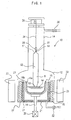
- Fig. 1 is a schematic view of an apparatus for manufacturing a single crystal by CZ method, in which a magnetic field applied apparatus is installed, for conducting a method of manufacturing a silicon single crystal according to the present invention.
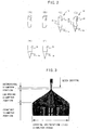
- Fig. 2 is a drawing showing seed crystals used in Dash Necking method, and seed crystals, each of which has a tip end with a sharp-pointed shape or a truncation thereof used in the manufacturing method of the present invention.
- Fig. 3 is a photograph showing a portion of a silicon single crystal having a crystal orientation of ⁇ 110> and a diameter of about 200 mm grown by means of the manufacturing method of the present invention.
- Fig. 4 is a drawing for illustrating removal of slip dislocations by Dash Necking method.
- FIGs. 2(C), 2(D), 2(E) and 2(F) are schematic views showing each seed crystal having a tip end with a sharp-pointed shape or a truncation thereof used in growth of silicon single crystals according to the present invention.
- Fig. 2(C) shows a seed crystal 1c having a cylindrical straight body 3c with a conical tip end 4c
- Fig. 2(D) shows a seed crystal 1d having a prismatic straight body 3d with a pyramidal tip end 4d.
- FIG. 2(E) and 2(F) shows a tip end of a seed crystal having a shape in which the tip end 4c of the seed crystal shown in Fig. 2(C) is truncated.
- Fig. 2(E) shows a tip end 4e in which the tip end 4c of the seed crystal 1c is horizontally truncated
- Fig. 2(F) shows a tip end 4f in which the tip end 4c is obliquely truncated.
- seed crystals having shapes of truncated tip end if the areas of the bottom parts of the tip ends 4e and 4f shown in Figs. 2(E) and 2(F) respectively are too large, thermal shock is likely to occur when the seed crystals come into contact with a melt. Therefore it is preferable that the area of a seed crystal which first comes into contact with silicon melt is 5 mm 2 or less.
- an angle of the tip end of the seed crystal refers to an apical angle of the tip end of the seed crystal when assuming a shape of the tip end before the tip end 4c is truncated.
- seed crystals are used in manufacturing a single crystal so that each of the straight bodies 3c and 3d of the seed crystals may be locked in a seed holder 28 of an apparatus 10 for manufacturing a single crystal shown in Fig. 1 via a locking part 2c or 2d provided on the straight body 3c or 3d, respectively.
- the tip ends 4c - 4f of the seed crystals have sharp-pointed shapes or truncations thereof so that slip dislocations may not be introduced into the seed crystals by thermal shock when the seed crystal comes into contact with a silicon melt, or even if they are introduced, the amount thereof may be a little. They have obviously different shapes from seed crystals used in Dash Necking method.
- Fig. 2(A) shows an approximately columnar seed crystal
- Fig. 2(B) shows a prismatic seed crystal
- the single crystal is grown by use of a seed crystal having the same crystal orientation as the single crystal to be grown.
- a seed crystal having a crystal orientation of ⁇ 110> in the direction of a pulling axis can be used.
- the seed crystal 1c or 1d shown in Fig. 2 is heated to approximately the same temperature as the silicon melt M just above the melt. After the temperature of the seed crystal becomes steady, the tip end 4c, 4d or 4e, 4f is gently dipped into the silicon melt M. When the tip end is dipped up to a desired diameter, then pulling is started. Thereby, a silicon single crystal S having an arbitrary decreasing diameter portion S0 shown in Fig.1 is grown.
- Fig. 1 is a schematic view showing an apparatus for manufacturing a silicon single crystal by a method of the present invention.
- An apparatus 10 for manufacturing a single crystal is composed of a growing furnace 12 where a silicon melt M is kept and growth of a single crystal is conducted, and an upper growing furnace 14 for storing and taking out a silicon single crystal S pulled from the silicon melt M.
- a winding and rotating mechanism 26 for rotating and pulling the single crystal when growing the crystal is installed.
- a seed holder 28 for locking a seed crystal 27 (the seed crystal 1c or 1d shown in Fig. 2 as an example) is located.
- the wire 24 is wound off from the winding and rotating mechanism 26, and a tip end of the seed crystal is dipped into the silicon melt M up to a desired position, and then the seed crystal 27 is pulled with being rotated at the predetermined rate. Thereby, the silicon single crystal S is grown below the seed crystal 27.
- a crucible 18 for containing the silicon melt M is installed inside the growing furnace 12. Since it contains the silicon melt M having a high temperature, the inside of the crucible 18 consists of a crucible made of quartz 18a, and the outside thereof consists of a crucible made of graphite 18b for protecting the crucible made of quartz 18a.
- the crucible 18 is disposed at the approximate center of the growing furnace 12 by a crucible supporting shaft 16. Beneath the crucible supporting shaft 16, a crucible driving mechanism 20 is mounted in order to keep a melt surface constant when growing a single crystal, and in order to grow a crystal with rotating the crucible 18 in CZ method or MCZ method.
- a heater made of graphite 23 for melting polycrystalline silicon as a raw material and keeping it as the silicon melt M is disposed outside the crucible 18, and an operation is performed while keeping a temperature of the silicon melt M at a temperature appropriate for growth of a crystal by controlling the amount of heat from the heater 23.
- heat insulators 22 and bottom heat insulators 21 are disposed, which keep the inside of the growing furnace 12 hot, and at the same time prevent a wall of the growing furnace 12 from directly being exposed to radiation heat from the heater 23.
- electromagnet 33 which is an apparatus for applying a horizontal magnetic field to the silicon melt M, is mounted outside the growing furnace 12.
- the center of the horizontal magnetic field is positioned inside the silicon melt M to efficiently suppress change in temperature of the melt, and the horizontal magnetic field having intensity of 1000 G or more at the center of the magnetic field, which is a desired magnetic intensity, can be obtained inside the silicon melt M when the seed crystal 27 is dipped.
- a gas flow controlling device 30 for controlling a flow rate of the inert gas flowing inside the manufacturing apparatus 10 is installed in the upper growing furnace 14, and a pressure controlling device 32 for adjusting the internal pressure is installed at the bottom of the growing furnace 12.
- the flow rate of the inert gas flowing in the apparatus 10 of manufacturing a single crystal and the pressure thereof are adjusted by use of these devices in accordance with growth conditions of a single crystal.
- polycrystalline silicon as a raw material is charged into the crucible 18, and the polycrystalline silicon is melted by heating from the heater 23.
- a temperature of the silicon melt M is decreased to that appropriate for growth of a single crystal.
- application of a magnetic field starts so that the horizontal magnetic field with the magnetic field intensity of 1000 G or more at the center may be applied to the silicon melt M by means of the electromagnet 33.
- This magnetic field is applied at least between the time when the tip end of the seed crystal 27 comes into contact with the silicon melt M and the time when formation of the decreasing diameter portion S0 formed below the seed crystal 27 finishes and the enlargement of a diameter of the crystal starts.
- the seed crystal 27 having an apical angle of the tip end of 28 ° or less is lowered to directly above the silicon melt M after the temperature becomes steady, and then stays until the temperature of the tip end of the seed crystal 27 is heated to approximately the same temperature as the silicon melt M.
- the seed crystal 27 is heated to approximately the same temperature as the silicon melt M, and further a temperature of a surface of the silicon melt M around the center of the crucible 18 into which the seed crystal S is dipped is stabilized to the extent that the temperature is changed in the range of ⁇ 5 °C or less, the seed crystal 27 is gently brought into contact with the silicon melt M and dipped thereinto.
- the temperature variation of the surface at the portion of the silicon melt M where the seed crystal S is dipped is kept in the range of ⁇ 5 °C or less, preferably ⁇ 3°C or less, at least until the tip end of the seed crystal 27 is brought into contact with the silicon melt M and then it shifts to pulling.
- the descending rate of the seed crystal 27 is decreased to be stopped when the tip end is immersed into the silicon melt M to the predetermined diameter, and then it shifts to pulling while adjusting the ascending rate of the seed crystal 27 and the temperature of the silicon melt.
- the crystal is formed while indicating a tendency that the diameter of the crystal to be grown at the bottom of the seed crystal 27 becomes smaller than the diameter of the tip end after immersion of the tip end of the seed crystal. If the diameter of the crystal is forcedly enlarged at that time, disadvantage may occur, for example, slip dislocations may be introduced into the seed crystal 27, or the growing crystal may be separated from the melt. Therefore, immediately after converting from dipping into pulling, it is necessary to perform pulling with adjusting the pulling rate so that the diameter of the crystal formed at the tip end of the seed crystal 27 may become slightly smaller than the immersion diameter of the tip end portion of the dipped seed crystal 27 (formation of the decreasing diameter portion S0). It is desirably pulled with keeping the pulling rate at this time at 0.5 mm/min or less.
- the diameter of the single crystal S formed below the seed crystal 27 through the enlarging diameter process is enlarged to the desired diameter, and the formation of the enlarging diameter portion S1 is stopped when it reaches the predetermined diameter. Then the pulling rate and/or the temperature of the melt are adjusted again to lead into formation of a constant diameter portion S2 of the single crystal.
- the constant diameter portion S2 is pulled to be the predetermined length while adjusting operation conditions in conformity to quality of the crystal to be grown and ambience inside the furnace (formation of the constant diameter portion S2).
- the growth conditions (a pulling rate, a temperature of a melt, etc.) is changed at the point when the formation of the constant diameter portion S2 having the predetermined length has been completed, and the diameter of the crystal is gradually decreased to form a tail portion S3 (formation of the tail portion S3).
- the grown crystal is separate from the silicon melt M, and is wound up to the upper growing furnace 14.
- the silicon crystal S is taken out from the apparatus 10 for manufacturing a single crystal to its outside after the temperature of the crystal lowers to a room temperature, and thereby growth is finished.
- the single crystal grown in accordance with the above-mentioned method is subjected to cutting/cylindrical grinding process and then it is processed into a wafer having a mirror-surface by the well-known method, a silicon wafer which is a main material for producing a semiconductor device can be obtained.
- a silicon single crystal having a diameter of approximately 150 mm (6 inches) in a constant diameter portion of the crystal was manufactured using an apparatus for manufacturing a silicon single crystal shown in Fig. 1 and adopting a pulling method using Dash Necking method without applying a magnetic field to a silicon melt.
- a seed crystal in order to grow a silicon single crystal while eliminating dislocations by Dash Necking method, there was used a seed crystal having a prismatic shape with sides of 15 mm and a crystal orientation of ⁇ 110> (a seed crystal having a shape shown in Fig. 2(b)) in which a surface for contacting with the silicon melt was flat.
- a crucible made of quartz and having a bore diameter of 450 mm was installed in an apparatus for manufacturing a silicon single crystal, and 60 kg of polycrystalline silicon as a raw material was filled into the crucible. After gas inside the manufacturing apparatus was exchanged for argon (Ar) gas, a heater made of carbon was heated to make the polycrystalline silicon a silicon melt.
- Ar argon
- dopant was introduced so that a crystal to be grown might be p-type and might have a resistivity of about 10 ⁇ cm. Then the melt was left until the temperature of the melt became steady, while the temperature of the silicon melt was adjusted so as to lower to the temperature appropriate to growth of a single crystal. In the meantime, operation conditions such as the amount of inert gas (Ar gas) flowing in the manufacturing apparatus, pressure therein and rotation of the crucible were adjusted to the manufacturing conditions for growing a single crystal until the temperature of the melt became steady.
- Ar gas inert gas
- Stability of the temperature of the melt was checked by measuring a surface temperature of the melt at the center of the crucible into which the seed crystal was dipped by use of a radiation thermometer (manufactured by CHINO, IR-02C), through a glass window provided to observe the inside of the manufacturing apparatus from the outside of the apparatus for manufacturing a single crystal. When a temperature appropriate to growth of a silicon crystal seemed to be obtained, the temperature was measured.
- a single crystal having a diameter of about 200 mm (8 inches) at a constant diameter portion was practically pulled in order to confirm whether a single crystal having a large diameter could be grown by a method for growing a dislocation-free silicon single crystal using a seed crystal having a sharp-pointed tip end without using Dash Necking method (hereinafter, referred to as dislocation-free seeding method).
- dopant was introduced into the melt so that resistivity of a p-type crystal might be a value of about 10 ⁇ cm. Then operation conditions such as Ar gas flow and pressure inside the manufacturing apparatus were adjusted, and it was left until the temperature became steady.
- a seed crystal used in Experiment 2 since there was a need to perform pulling while avoiding introduction of slip dislocations due to thermal shock without using Dash Necking, a seed crystal having a shape shown in Fig. 2(C), which had a columnar straight body with a diameter of 15 mm and a sharp conical tip end with an apical angle of 15 °, was used.
- the seed crystal was gently lowered to 1 mm directly above a surface of the silicon melt and heated for about 20 minutes till the temperature of the seed crystal became approximately the same as the temperature of the melt. Thereafter the seed crystal was brought into contact with the silicon melt and immersed into the melt to the desired diameter, and then the seed crystal was gradually pulled while keeping the pulling rate at 0.5 mm/min or less. Thereby formation of a silicon single crystal below the seed crystal was tried.
- the diameter was enlarged to 200 mm after the seed crystal was dipped to the predetermined length and subsequently a decreasing diameter portion was formed, and then judgment on nonexistence of dislocations was conducted by checking crystal habit lines indicating a condition of a single crystal.
- This is a general method in which crystallization of a single crystal can be easily judged since a characteristic crystal habit to be generated on a surface of a single crystal disappears in the case that dislocations remain in the seed crystal.
- a seed crystal a seed crystal having a shape shown in Fig. 2(c) was used, which had a columnar straight body with a diameter of 15 mm and a sharp conical tip end with an apical angle of 15 °.
- Example 1 application of the magnetic field was continued from the time when the melting was finished and stabilization of the temperature of the melt was set out until the time when the growth of the silicon single crystal was finished and a tail portion of the crystal was separated from the melt.
- the seed crystal was gently lowered to 1 mm directly above the silicon melt, and it was left for about 20 minutes until the seed crystal was heated. Then after the seed crystal was heated to the temperature as much as the temperature of the silicon melt, the tip end of the seed crystal was gradually lowered into the melt and the conical portion of the tip end of the seed crystal (the tip end portion) was immersed into the silicon melt up to a desired diameter.
- the diameter of the crystal was gradually lessened to form a tail portion and the grown crystal was separated from the silicon melt. Thereby the growth of the silicon single crystal had been finished.
- the grown silicon single crystal was gently cooled, and it was taken out of the manufacturing apparatus.
- a heavy single crystal with a large diameter shown in Fig. 3 was obtained, which had a diameter of 208 mm and weight of 120 kg.
- there was no failure such that a crystal was grown again from the beginning due to introduction of slip dislocations during growth, and therefore it was possible to grow a heavy single crystal with a large diameter which was dislocation-free and had an intended crystal orientation of ⁇ 110> without any difficulty.
- the minimum diameter of the decreasing diameter portion formed at the tip end of the seed crystal shown in Fig. 3 was 5 mm or more, and therefore a single crystal could be grown without using Dash Necking method.
- the embodiments of the present invention were explained with referring to an example of growing a silicon single crystal having a diameter of 200 mm (8 inches), however, the effects of the present invention can be sufficiently obtained also in the case of growing a silicon single crystal having a smaller diameter. Further the present invention is also effective in increasing the weight since there is no need to perform necking of a seed crystal by Dash Necking method.
- the present invention since the diameter of 5 mm or more can be ensured even at the minimum diameter portion of a crystal formed at the tip end of a seed crystal, the present invention can be also applied to manufacture of a silicon single crystal with a large diameter of 300 mm (12 inches) or more which have been widely utilized in recent years, particularly, a heavy silicon single crystal having weight of the crystal over 300 kg.
Landscapes
- Chemical & Material Sciences (AREA)
- Engineering & Computer Science (AREA)
- Crystallography & Structural Chemistry (AREA)
- Materials Engineering (AREA)
- Metallurgy (AREA)
- Organic Chemistry (AREA)
- Crystals, And After-Treatments Of Crystals (AREA)
Abstract
Description
| (Results of growing a silicon single crystal having a crystal orientation of <110>) | ||||||
| Intensity of applied magnetic field (horizontal magnetic field) | Diameter of grown crystal | Method for necking | The number of failure in seeding | Range of temperature variation of melt | Presence or absence of success in pulling a crystal | |
| Experiment 1 | Not applied | 15 cm | Dash Necking method | 6 times | ± 6 ° | X |
| Experiment | ||||||
| 2 | Not applied | 20 cm | Dislocation-free seeding method | 9 times | ± 8 °C | X |
| Example 1 | 4000 | 20 cm | Dislocation-free seeding method | 0 time | ±1.5°C | O |
| (Results of dislocation generation in a silicon seed crystal having a crystal orientation of <110>) | |||||
| Intensity of applied magnetic field (horizontal magnetic field) | Bore of quartz crucible | The amount of silicon melt | Range of temperature variation of melt | State of | |
| Experiment | |||||
| 3 | 500 G | 600 mm | 150 kg | ± 10 °C | Presence of |
| Experiment | |||||
| 4 | 750 G | 600 mm | 150 kg | ± 5.6°C | Presence of |
| Experiment | |||||
| 5 | 0 G | 600 mm | 150 kg | ± 4.3°C | Absence of dislocation |
Claims (7)
- A method of manufacturing a silicon single crystal by Czochralski method without performing Dash Necking method, comprising the steps of:wherein a temperature variation at a surface of the silicon melt is kept at ±5°C or less at least for a period from a point of bringing the tip end of the seed crystal into contact with the silicon melt to a point of shifting to pull the single crystal.providing a seed crystal having a tip end with a sharp-pointed shape or a truncation thereof in which an angle of the tip end is 28 ° or less;keeping the tip end of the seed crystal at just above a silicon melt to heat it before bringing the tip end of the seed crystal into contact with the silicon melt;subsequently, bringing the tip end of the seed crystal into contact with the silicon melt and immersing the seed crystal into the silicon melt to a desired diameter; and thenshifting to pull the single crystal,
- The method of manufacturing a silicon single crystal according to claim 1, wherein the seed crystal is brought into contact with the silicon melt and immersed therein with setting a temperature of the silicon melt when bringing the tip end of the seed crystal into contact with the silicon melt to 10 - 20 °C higher than a temperature appropriate for bringing the seed crystal into contact with the silicon melt in a method of manufacturing a silicon single crystal using Dash Necking method, and the single crystal is pulled with setting a pulling rate to 0.5 mm/min or less at least when forming a decreasing diameter portion for a period from a point immediately after stopping lowering of the seed crystal and shifting to pulling to a point of starting enlargement of a diameter of the crystal formed below the seed crystal.
- The method of manufacturing a silicon single crystal according to claim 2, wherein the single crystal is pulled while a horizontal magnetic field with a magnetic field intensity of 1000 G or more at a center thereof is applied to the silicon melt at least for a period from a point of bringing the tip end of the seed crystal into contact with the silicon melt to a point of completing formation of a decreasing diameter portion formed below the seed crystal and starting enlargement of the diameter of the crystal.
- The method of manufacturing a silicon single crystal according to any one of claims 1-3, wherein a silicon single crystal having a crystal orientation of <110> is pulled by using a seed crystal having a crystal orientation of <110>.
- A silicon single crystal grown by Czochralski method, which has a crystal orientation of <110>, and a constant diameter portion with a diameter of 200 mm or more.
- The silicon single crystal according to claim 5, wherein total weight of the single crystal pulled from the silicon melt is 100 kg or more.
- A silicon wafer, wherein a main diameter of the wafer is 200 mm or more, and a plane orientation of a main surface of the wafer is (110).
Applications Claiming Priority (3)
| Application Number | Priority Date | Filing Date | Title |
|---|---|---|---|
| JP2002122250 | 2002-04-24 | ||
| JP2002122250 | 2002-04-24 | ||
| PCT/JP2003/005167 WO2003091483A1 (en) | 2002-04-24 | 2003-04-23 | Method for producing silicon single crystal and, silicon single crystal and silicon wafer |
Publications (3)
| Publication Number | Publication Date |
|---|---|
| EP1498517A1 true EP1498517A1 (en) | 2005-01-19 |
| EP1498517A4 EP1498517A4 (en) | 2008-09-17 |
| EP1498517B1 EP1498517B1 (en) | 2016-08-31 |
Family
ID=29267437
Family Applications (1)
| Application Number | Title | Priority Date | Filing Date |
|---|---|---|---|
| EP03719172.3A Expired - Lifetime EP1498517B1 (en) | 2002-04-24 | 2003-04-23 | Method of manufacturing silicon single crystal |
Country Status (7)
| Country | Link |
|---|---|
| US (2) | US7179330B2 (en) |
| EP (1) | EP1498517B1 (en) |
| JP (1) | JP4151580B2 (en) |
| KR (1) | KR100987470B1 (en) |
| CN (1) | CN1323196C (en) |
| TW (1) | TW200305664A (en) |
| WO (1) | WO2003091483A1 (en) |
Cited By (2)
| Publication number | Priority date | Publication date | Assignee | Title |
|---|---|---|---|---|
| EP4428272A1 (en) | 2023-03-10 | 2024-09-11 | Siltronic AG | Method of drawing a single crystal ingot of semiconductor material and a wafer of semiconductor material |
| EP4524296A1 (en) | 2023-09-13 | 2025-03-19 | Siltronic AG | Method for pulling single crystal ingot |
Families Citing this family (19)
| Publication number | Priority date | Publication date | Assignee | Title |
|---|---|---|---|---|
| CN100585031C (en) * | 2006-12-06 | 2010-01-27 | 天津市环欧半导体材料技术有限公司 | <110> Manufacturing method of dislocation-free silicon single crystal |
| JP4946590B2 (en) * | 2007-04-19 | 2012-06-06 | 株式会社Sumco | Silicon single crystal growth method, evaluation method and production method |
| JP5083001B2 (en) * | 2008-04-08 | 2012-11-28 | 株式会社Sumco | Pulling method of silicon single crystal |
| JP4862884B2 (en) * | 2008-05-21 | 2012-01-25 | 信越半導体株式会社 | Method for producing silicon single crystal |
| JP5229017B2 (en) * | 2009-03-11 | 2013-07-03 | 信越半導体株式会社 | Single crystal manufacturing method |
| WO2011010394A1 (en) * | 2009-07-21 | 2011-01-27 | トヨタ自動車株式会社 | Seed-crystal shaft for single-crystal growth by solution method |
| JP5482547B2 (en) * | 2010-07-30 | 2014-05-07 | 信越半導体株式会社 | Method for producing silicon single crystal |
| CN102134739A (en) * | 2011-03-08 | 2011-07-27 | 宁夏日晶新能源装备股份有限公司 | Automatic crystal guide system of single crystal furnace, and automatic crystal guide method |
| CN102181916B (en) * | 2011-03-29 | 2013-04-10 | 浙江晨方光电科技有限公司 | Method for improving uniformity of resistivity in N type 111 crystal direction |
| GB2497120A (en) * | 2011-12-01 | 2013-06-05 | Rec Wafer Norway As | Production of mono-crystalline silicon |
| JP5660020B2 (en) | 2011-12-16 | 2015-01-28 | 信越半導体株式会社 | Method for producing silicon single crystal |
| JP5819185B2 (en) * | 2011-12-29 | 2015-11-18 | グローバルウェーハズ・ジャパン株式会社 | Method for producing silicon single crystal |
| US9102035B2 (en) * | 2012-03-12 | 2015-08-11 | MEMC Electronics Materials S.p.A. | Method for machining seed rods for use in a chemical vapor deposition polysilicon reactor |
| US20150044467A1 (en) * | 2012-04-23 | 2015-02-12 | Hwajin Jo | Method of growing ingot and ingot |
| JP5831436B2 (en) | 2012-12-11 | 2015-12-09 | 信越半導体株式会社 | Method for producing silicon single crystal |
| CN103436954A (en) * | 2013-09-11 | 2013-12-11 | 英利能源(中国)有限公司 | Seed crystal for seeding during manufacturing of silicon single crystal rod and manufacturing method of silicon single crystal rod |
| DE102017215332A1 (en) * | 2017-09-01 | 2019-03-07 | Fraunhofer-Gesellschaft zur Förderung der angewandten Forschung e.V. | A single crystal of <100> oriented silicon doped with n-type dopant and methods of producing such a single crystal |
| CN111139520A (en) * | 2018-11-05 | 2020-05-12 | 上海新昇半导体科技有限公司 | Seeding method by Czochralski method |
| JP7124938B1 (en) | 2021-07-29 | 2022-08-24 | 信越半導体株式会社 | Manufacturing method of silicon single crystal |
Family Cites Families (23)
| Publication number | Priority date | Publication date | Assignee | Title |
|---|---|---|---|---|
| US4002523A (en) * | 1973-09-12 | 1977-01-11 | Texas Instruments Incorporated | Dislocation-free growth of silicon semiconductor crystals with <110> orientation |
| JPH01203287A (en) | 1988-02-08 | 1989-08-16 | Nec Corp | Method for pulling up single crystal |
| US4891255A (en) * | 1988-09-29 | 1990-01-02 | The United States Of America As Represented By The United States Department Of Energy | (110) Oriented silicon wafer latch accelerometer and process for forming the same |
| JP2601930B2 (en) * | 1990-03-29 | 1997-04-23 | 信越半導体株式会社 | Method and apparatus for controlling diameter of single crystal neck |
| DE4106589C2 (en) * | 1991-03-01 | 1997-04-24 | Wacker Siltronic Halbleitermat | Continuous recharge with liquid silicon during crucible pulling according to Czochralski |
| US5487355A (en) * | 1995-03-03 | 1996-01-30 | Motorola, Inc. | Semiconductor crystal growth method |
| JP3841863B2 (en) * | 1995-12-13 | 2006-11-08 | コマツ電子金属株式会社 | Method of pulling silicon single crystal |
| US5840120A (en) * | 1996-01-22 | 1998-11-24 | Memc Electronic Materials, Inc. | Apparatus for controlling nucleation of oxygen precipitates in silicon crystals |
| US6217663B1 (en) * | 1996-06-21 | 2001-04-17 | Kokusai Electric Co., Ltd. | Substrate processing apparatus and substrate processing method |
| JPH10101482A (en) * | 1996-10-01 | 1998-04-21 | Komatsu Electron Metals Co Ltd | Production unit for single crystal silicon and its production |
| JPH10203898A (en) * | 1997-01-17 | 1998-08-04 | Shin Etsu Handotai Co Ltd | Production of silicon single crystal and seed crystal |
| DE69802864T2 (en) * | 1997-05-21 | 2002-08-29 | Shin-Etsu Handotai Co., Ltd. | Silicon seed crystal, method of manufacturing the same, and method of manufacturing a silicon single crystal using the silicon seed crystal |
| JP3387364B2 (en) | 1997-05-21 | 2003-03-17 | 信越半導体株式会社 | Silicon seed crystal, method for producing the same, and method for producing silicon single crystal using these seed crystals |
| JP3684769B2 (en) * | 1997-06-23 | 2005-08-17 | 信越半導体株式会社 | Method for producing and holding silicon single crystal |
| JP3440802B2 (en) * | 1998-01-14 | 2003-08-25 | 信越半導体株式会社 | Method for producing silicon single crystal |
| JP2000203287A (en) * | 1999-01-13 | 2000-07-25 | Toyota Motor Corp | Power output device and hybrid vehicle having the same |
| DE19938340C1 (en) * | 1999-08-13 | 2001-02-15 | Wacker Siltronic Halbleitermat | Production of semiconductor wafer comprises simultaneously polishing the front and rear sides of wafer between rotating polishing plates using an alkaline polishing sol and then an alcohol, cleaning, drying and applying an epitaxial layer |
| US6869477B2 (en) * | 2000-02-22 | 2005-03-22 | Memc Electronic Materials, Inc. | Controlled neck growth process for single crystal silicon |
| US6506251B1 (en) * | 2000-02-25 | 2003-01-14 | Shin-Etsu Handotai Co., Ltd. | Method for producing silicon single crystal |
| JP4808832B2 (en) * | 2000-03-23 | 2011-11-02 | Sumco Techxiv株式会社 | Method for producing defect-free crystals |
| DE10052411B4 (en) * | 2000-10-23 | 2008-07-31 | Mitsubishi Materials Silicon Corp. | Heat treatment method of a silicon wafer and the heat-treated silicon wafer |
| JP3994665B2 (en) * | 2000-12-28 | 2007-10-24 | 信越半導体株式会社 | Silicon single crystal wafer and method for producing silicon single crystal |
| JP4215249B2 (en) * | 2003-08-21 | 2009-01-28 | コバレントマテリアル株式会社 | Method for producing silicon seed crystal and silicon single crystal |
-
2003
- 2003-04-23 WO PCT/JP2003/005167 patent/WO2003091483A1/en not_active Ceased
- 2003-04-23 KR KR1020047016852A patent/KR100987470B1/en not_active Expired - Lifetime
- 2003-04-23 US US10/510,695 patent/US7179330B2/en not_active Expired - Lifetime
- 2003-04-23 JP JP2003588003A patent/JP4151580B2/en not_active Expired - Fee Related
- 2003-04-23 EP EP03719172.3A patent/EP1498517B1/en not_active Expired - Lifetime
- 2003-04-23 CN CNB038089580A patent/CN1323196C/en not_active Expired - Lifetime
- 2003-04-24 TW TW092109624A patent/TW200305664A/en not_active IP Right Cessation
-
2007
- 2007-01-04 US US11/620,024 patent/US20070101926A1/en not_active Abandoned
Cited By (4)
| Publication number | Priority date | Publication date | Assignee | Title |
|---|---|---|---|---|
| EP4428272A1 (en) | 2023-03-10 | 2024-09-11 | Siltronic AG | Method of drawing a single crystal ingot of semiconductor material and a wafer of semiconductor material |
| WO2024188617A1 (en) | 2023-03-10 | 2024-09-19 | Siltronic Ag | Method for pulling a single crystal ingot of semiconductor material, and wafer of semiconductor material |
| EP4524296A1 (en) | 2023-09-13 | 2025-03-19 | Siltronic AG | Method for pulling single crystal ingot |
| WO2025056242A1 (en) | 2023-09-13 | 2025-03-20 | Siltronic Ag | Method for pulling a single-crystal ingot |
Also Published As
| Publication number | Publication date |
|---|---|
| JP4151580B2 (en) | 2008-09-17 |
| JPWO2003091483A1 (en) | 2005-09-02 |
| EP1498517B1 (en) | 2016-08-31 |
| TWI324643B (en) | 2010-05-11 |
| CN1323196C (en) | 2007-06-27 |
| EP1498517A4 (en) | 2008-09-17 |
| KR20040104569A (en) | 2004-12-10 |
| WO2003091483A1 (en) | 2003-11-06 |
| KR100987470B1 (en) | 2010-10-13 |
| US20050160966A1 (en) | 2005-07-28 |
| TW200305664A (en) | 2003-11-01 |
| US7179330B2 (en) | 2007-02-20 |
| CN1646736A (en) | 2005-07-27 |
| US20070101926A1 (en) | 2007-05-10 |
Similar Documents
| Publication | Publication Date | Title |
|---|---|---|
| US7179330B2 (en) | Method of manufacturing silicon single crystal, silicon single crystal and silicon wafer | |
| US7611580B2 (en) | Controlling melt-solid interface shape of a growing silicon crystal using a variable magnetic field | |
| US20080184929A1 (en) | Single crystal pulling apparatus | |
| JP2003313089A (en) | Method for manufacturing single crystal silicon and single crystal silicon wafer, seed crystal for manufacturing single crystal silicon, single crystal silicon ingot, and single crystal silicon wafer | |
| KR100717237B1 (en) | Process for producing single crystal silicon with uniform thermal history | |
| CN113272479B (en) | Controlling dopant concentration in silicon melt to enhance ingot quality | |
| JP2017222551A (en) | Method for producing silicon single crystal | |
| EP1614774A1 (en) | Process for producing single crystal | |
| JP2003286024A (en) | Unidirectionally solidified silicon ingot, its manufacturing method, silicon plate, solar cell substrate, and sputtering target material | |
| KR20080006013A (en) | Silicon Single Crystal Growth Method and Silicon Wafer Manufacturing Method | |
| CN114616361B (en) | Manufacturing method of silicon single crystal | |
| KR101609465B1 (en) | Apparatus of growth of silicon single crystal ingot | |
| JPH10167881A (en) | Method for pulling semiconductor single crystal | |
| JP4341379B2 (en) | Single crystal manufacturing method | |
| TWI751028B (en) | Method for manufacturing single crystal silicon | |
| JP4899608B2 (en) | Semiconductor single crystal manufacturing apparatus and manufacturing method | |
| KR20090008969A (en) | Silicon Single Crystal Growth Apparatus and Silicon Single Crystal Growth Method | |
| KR101472354B1 (en) | Methof for manefacturing silicon single crystal and silicon single crystal ingot |
Legal Events
| Date | Code | Title | Description |
|---|---|---|---|
| PUAI | Public reference made under article 153(3) epc to a published international application that has entered the european phase |
Free format text: ORIGINAL CODE: 0009012 |
|
| 17P | Request for examination filed |
Effective date: 20041019 |
|
| AK | Designated contracting states |
Kind code of ref document: A1 Designated state(s): AT BE BG CH CY CZ DE DK EE ES FI FR GB GR HU IE IT LI LU MC NL PT RO SE SI SK TR |
|
| A4 | Supplementary search report drawn up and despatched |
Effective date: 20080821 |
|
| RIC1 | Information provided on ipc code assigned before grant |
Ipc: C30B 29/06 20060101AFI20031112BHEP Ipc: C30B 15/36 20060101ALI20080814BHEP Ipc: C30B 15/22 20060101ALI20080814BHEP |
|
| RAP1 | Party data changed (applicant data changed or rights of an application transferred) |
Owner name: SHIN-ETSU HANDOTAI CO., LTD. |
|
| 17Q | First examination report despatched |
Effective date: 20100601 |
|
| RAP1 | Party data changed (applicant data changed or rights of an application transferred) |
Owner name: SHIN-ETSU HANDOTAI CO., LTD. |
|
| GRAP | Despatch of communication of intention to grant a patent |
Free format text: ORIGINAL CODE: EPIDOSNIGR1 |
|
| INTG | Intention to grant announced |
Effective date: 20160314 |
|
| GRAS | Grant fee paid |
Free format text: ORIGINAL CODE: EPIDOSNIGR3 |
|
| GRAA | (expected) grant |
Free format text: ORIGINAL CODE: 0009210 |
|
| AK | Designated contracting states |
Kind code of ref document: B1 Designated state(s): DE |
|
| REG | Reference to a national code |
Ref country code: DE Ref legal event code: R096 Ref document number: 60349337 Country of ref document: DE |
|
| REG | Reference to a national code |
Ref country code: DE Ref legal event code: R097 Ref document number: 60349337 Country of ref document: DE |
|
| PLBE | No opposition filed within time limit |
Free format text: ORIGINAL CODE: 0009261 |
|
| STAA | Information on the status of an ep patent application or granted ep patent |
Free format text: STATUS: NO OPPOSITION FILED WITHIN TIME LIMIT |
|
| 26N | No opposition filed |
Effective date: 20170601 |
|
| PGFP | Annual fee paid to national office [announced via postgrant information from national office to epo] |
Ref country code: DE Payment date: 20220302 Year of fee payment: 20 |
|
| REG | Reference to a national code |
Ref country code: DE Ref legal event code: R071 Ref document number: 60349337 Country of ref document: DE |