EP1496548A1 - Method for manufacturing differential isolation structures in a semiconductor electronic device and corresponding structure - Google Patents
Method for manufacturing differential isolation structures in a semiconductor electronic device and corresponding structure Download PDFInfo
- Publication number
- EP1496548A1 EP1496548A1 EP03425459A EP03425459A EP1496548A1 EP 1496548 A1 EP1496548 A1 EP 1496548A1 EP 03425459 A EP03425459 A EP 03425459A EP 03425459 A EP03425459 A EP 03425459A EP 1496548 A1 EP1496548 A1 EP 1496548A1
- Authority
- EP
- European Patent Office
- Prior art keywords
- area
- active areas
- layer
- isolation structures
- structure according
- Prior art date
- Legal status (The legal status is an assumption and is not a legal conclusion. Google has not performed a legal analysis and makes no representation as to the accuracy of the status listed.)
- Granted
Links
Images








Classifications
-
- H—ELECTRICITY
- H10—SEMICONDUCTOR DEVICES; ELECTRIC SOLID-STATE DEVICES NOT OTHERWISE PROVIDED FOR
- H10W—GENERIC PACKAGES, INTERCONNECTIONS, CONNECTORS OR OTHER CONSTRUCTIONAL DETAILS OF DEVICES COVERED BY CLASS H10
- H10W10/00—Isolation regions in semiconductor bodies between components of integrated devices
- H10W10/01—Manufacture or treatment
- H10W10/011—Manufacture or treatment of isolation regions comprising dielectric materials
- H10W10/014—Manufacture or treatment of isolation regions comprising dielectric materials using trench refilling with dielectric materials, e.g. shallow trench isolations
- H10W10/0143—Manufacture or treatment of isolation regions comprising dielectric materials using trench refilling with dielectric materials, e.g. shallow trench isolations comprising concurrently refilling multiple trenches having different shapes or dimensions
-
- H—ELECTRICITY
- H10—SEMICONDUCTOR DEVICES; ELECTRIC SOLID-STATE DEVICES NOT OTHERWISE PROVIDED FOR
- H10W—GENERIC PACKAGES, INTERCONNECTIONS, CONNECTORS OR OTHER CONSTRUCTIONAL DETAILS OF DEVICES COVERED BY CLASS H10
- H10W10/00—Isolation regions in semiconductor bodies between components of integrated devices
- H10W10/10—Isolation regions comprising dielectric materials
- H10W10/17—Isolation regions comprising dielectric materials formed using trench refilling with dielectric materials, e.g. shallow trench isolations
Definitions
- the present invention relates to a method for manufacturing isolation structures in an electronic device.
- the invention relates to a method for manufacturing isolation structures of different thickness in a monolithically integrated semiconductor electronic device.
- the invention particularly relates to isolation structures of different thickness in a monolithically integrated semiconductor electronic device, and containing a matrix of non-volatile memory cells and an associated circuitry, reference being made in the following description to this field of application for convenience of explanation only.
- a monolithically integrated semiconductor electronic device consists of electrically active areas, commonly known as the active areas, and of electrically passive areas, commonly known as isolation areas. Active areas can be classified according to the type of electric structure that they contain. For example, there can be storage areas typically containing memory cells, and circuit areas typically containing transistors, capacitors and resistors.
- FIG. 1 A block diagram, not to scale, of a monolithically integrated semiconductor electronic device 10 and of advanced generation is shown in Figure 1 by way of example.
- This device which contains memory, circuit, and isolation areas not shown in Figure 1, typically has at least one circuit area 102 and at least one so-called matrix area 101, the latter comprising a plurality of memory cells being matrix-like arranged.
- the memory cells are arranged in rows, or word-lines, and columns, or bit-lines.
- this memory cell matrix Associated with this memory cell matrix is a plurality of transistors of the circuit area 102, which forms the control circuitry of the device.
- the isolation areas provided in the device 10 have the aim of isolating, electrically and physically, each active area from the others, and of reducing possible parasite effects. These isolation areas are usually formed simultaneously in different areas of the device 10, and appear in both the matrix and the circuit areas, 101 and 102.
- the isolation areas should have suitable sizes for memory cells in the matrix area 101 to be manufactured with a high density layout.
- Both the high density memory cells of the matrix area 101 and the transistors of the circuit area 102 must have, on the other side, an optimal behaviour.
- the reduction of isolation structure sizes, necessary to provide the matrix area 101 with high-density memory cells comes out in a lower reduction of the parasite effects in the circuit area 102, and in the consequent degradation of the transistor electrical performances.
- These problems impose to manufacture isolation structures of different thickness according to the device area being considered, a thickness which is to be smaller in the matrix area 101 than in the circuit area 102.
- These isolation structures of different thickness are defined as differential isolation.
- a prior art solution to obtain differential isolation structures 20 consists in manufacturing isolation structures, separately and by means of dedicated masks, these structures having different thickness and depths.
- this solution is exemplified by STI structures, and comprises the following steps:
- this solution has the drawback of requiring the repetition of some process steps with respect to what happens in the standard single-isolation flow process.
- the lithographic defining (B), nitride and pad oxide etching (C), silicon etching (D), and resist removing (E) steps in the above exemplary flow process are to be carried out a first time for the circuit area 102 and a second time for the matrix area 101.
- the mask employed during the lithographic defining step (B) is used a second time. A direct negative consequence of this solution stays in the increased cost and time requirements for manufacturing the isolation structures.
- An exemplary floating gate non-volatile memory cell to be typically comprised in the matrix area 101 of the device 10, is schematically shown, in cross section and not to scale, limited to its layers of concern in Figure 3, where the whole memory cell is indicated with reference number 30.
- This cell 30 comprises a source region 301, a drain region 302, and a succession of layers forming a gate region globally indicated with reference number 303.
- the gate region 303 comprises a first or floating gate layer 305 formed above the substrate of semiconductor material and separated from the latter by a thin dielectric layer 304, called tunnel oxide.
- a second or control gate layer 307 is capacitively coupled to the first floating gate layer 305 by a dielectric layer 306, called interpoly dielectric.
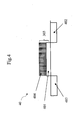
- An exemplary transistor 40 of the circuit area 102 is schematically shown, in cross section and not to scale, limited to its layers of concern in Figure 4.
- This transistor typically includes a gate region 303, comprising a gate layer 404 formed above the semiconductor material substrate and separated from the latter by a thin dielectric layer 401, called gate oxide.
- a source region 402 and a drain region 403 are integrated in the substrate of semiconductor material at the sides of the gate region 303.
- control gate layer 307 and the gate layer 404 are usually formed through a first step (G) of depositing the same polysilicon layer, a second step (I) of lithography defining, and a third step (J) of etching the polysilicon layer.
- the thickness of the layer succession under the polysilicon layer is different in the matrix 101 and circuit 102 area, typically higher in the matrix area 101 because of the presence of the floating gate layer 305 and the interpoly dielectric 306.
- the polysilicon layer is bound to be non-planar at the boundary of the matrix area 101. This unevenness causes possible lithographic defining problems resulting in the size and performance of those memory cells 30 which are located at the boundary of the matrix area 101.
- a first known solution solves this problem by performing a CMP (Chemical-Mechanical Polishing) step (H) after the polysilicon layer depositing step (G) to reduce the thickness of the polysilicon layer in the matrix area 101.
- CMP Chemical-Mechanical Polishing
- the lithographic defining step (I) of the polysilicon layer and the etching step (J) are then carried out.
- the above solution can have a drawback, due to the fact that the CMP technique applied during the etching step (H) needs, to be correctly and successfully performed, the layer to be etched to have an almost planar morphology. Accordingly to this solution, the different height of the polysilicon layer in the matrix areas 101 and in the circuit area 102 requires to maintain the polysilicon layer depositing step (G) until an almost planar morphology of the layer itself is achieved. In this way, however, a portion of the polysilicon layer of particularly high thickness is obtained in the circuit area 102, which brings about subsequent doping problems of that polysilicon portion.
- a second solution implies the polysilicon depositing step (G) to be followed by a masking step (L) exposing a portion of the polysilicon layer in the matrix area 101.
- An etching step (M), called etch-back, of the portion of the polysilicon layer in the matrix area 101 and a step (N) of removing the resist used in the above masking step (L) are then carried out. This is followed by the lithographic polysilicon layer defining step (I) and by the etching step (J).
- this solution shows integration problems because the etch-back step (M) is hard to control and can easily lead to an excessive reduction of the polysilicon layer thickness of the matrix area 101, with subsequent quality problems of the dielectric layers and possible device malfunctioning.
- the technical problem that underlies this invention is to provide a method for manufacturing a monolithically integrated semiconductor electronic device and of advanced generation, with such characteristics as to allow differential isolation structures to be formed and the gate regions accurately defined especially at the boundary of a memory cell matrix, thereby overcoming the limitations and/or drawbacks of prior art methods.
- the solution idea on which this invention stands is that of realising a digging in one or more areas of a monolithically integrated semiconductor electronic device. This digging is realised after a formation step of isolation structures in the device, and before forming and defining steps of electrically active layers above a starting substrate.
- a monolithically integrated semiconductor electronic device comprises at least a matrix area and at least a circuit area, and it comprises a structure 50 as shown schematically in cross-section, not to scale, in Figure 5 limited to concerned layers.
- the structure 50 exemplifies a device containing floating gate non-volatile flash memory cells.
- the structure 50 includes differential isolation structures 501 of the STI (Shallow Trench Isolation) type, active areas 502 of floating gate non-volatile flash memory cells, and active areas 503 of transistors.
- STI Shallow Trench Isolation
- active areas 502 of floating gate non-volatile flash memory cells and active areas 503 of transistors.
- Provided in the active areas 502 are a first tunnel oxide layer 506, a second floating gate layer 507, and a third interpoly dielectric layer 508.
- the differential isolation structures 501 are characterised by a bottom wall 504 extending at the same depth with respect to the surface 205 of the starting substrate in each area of the device.
- the active areas 502 and 503 are provided at a different depth with respect to the starting substrate surface 205. Accordingly, the morphology of a polysilicon layer 510 provided above the aforementioned layers is substantially planar.
- a preferred method for forming the structure 50 in accordance with the invention advantageously comprises the process steps described here below. The description includes only those commonly used process steps that are necessary to an understanding of this invention.
- differential isolation structures will now be described in detail with reference to Figures 6 to 9 and in relation, for example, to a monolithically integrated semiconductor electronic device which contains floating gate non-volatile flash memory cells and wherein the isolation structures are STI structures.
- the method of the invention comprises the steps listed here below, to be carried out in sequential order:
- This planar morphology advantageously provided by the inventive method, makes the lithografic defining of the gate regions in the circuit area 902 and the matrix area 901 easier to carry out in an optimum manner.
- the inventive method just described affords two advantages, being independent one another, in a monolithically integrated semiconductor electronic device.
- this method provides differential isolation structures in areas requiring isolation structures of different thickness, without requiring repetition, with respect to a standard single-isolation flow process, of a series of steps such as lithographic defining of active areas, dielectric layers etching, silicon etching, and resist removal. Furthermore, with respect to a standard single-isolation flow process, this method provides differential isolation structures without using an additional mask that is needed in the prior art.
- the method of this invention can be applied and it is advantageous whenever a monolithically integrated semiconductor electronic device is to be provided with isolation structures of different thickness in different areas, even when no floating gate layers are provided.
- the method of this invention is also effective to remove all current problems during lithographic defining of gate regions of memory cells and transistors, thereby overcoming the disadvantages of the prior art.
- the method of the invention may be applied and it is advantageous whenever planarity requires to be enhanced in the defining of one or more so-called pre-metal layers, that is layers formed over active areas before the electric contact and interconnection structures are formed.
- pre-metal layers that is layers formed over active areas before the electric contact and interconnection structures are formed.
- the structure according to this invention is highly advantageous also in the case of a monolithically integrated semiconductor electronic device, also not comprising floating-gate non-volatile memory cells, wherein areas involving the presence of different-thickness isolation structures and active devices with different heights with respect to a starting substrate are provided.
- the advantages of the inventive structure are to be appreciated when isolation structures of smaller thickness and active devices of greater height must be provided in one area with respect to another. In this case, in fact, the invention meets both requirements by a novel single structure.
Landscapes
- Non-Volatile Memory (AREA)
- Semiconductor Memories (AREA)
Abstract
Description
- The present invention relates to a method for manufacturing isolation structures in an electronic device.
- More particularly, the invention relates to a method for manufacturing isolation structures of different thickness in a monolithically integrated semiconductor electronic device.
- Although not limited to, the invention particularly relates to isolation structures of different thickness in a monolithically integrated semiconductor electronic device, and containing a matrix of non-volatile memory cells and an associated circuitry, reference being made in the following description to this field of application for convenience of explanation only.
- As it is known, a monolithically integrated semiconductor electronic device consists of electrically active areas, commonly known as the active areas, and of electrically passive areas, commonly known as isolation areas. Active areas can be classified according to the type of electric structure that they contain. For example, there can be storage areas typically containing memory cells, and circuit areas typically containing transistors, capacitors and resistors.
- A block diagram, not to scale, of a monolithically integrated semiconductor
electronic device 10 and of advanced generation is shown in Figure 1 by way of example. This device, which contains memory, circuit, and isolation areas not shown in Figure 1, typically has at least onecircuit area 102 and at least one so-calledmatrix area 101, the latter comprising a plurality of memory cells being matrix-like arranged. This means that the memory cells are arranged in rows, or word-lines, and columns, or bit-lines. - Associated with this memory cell matrix is a plurality of transistors of the
circuit area 102, which forms the control circuitry of the device. - The isolation areas provided in the
device 10 have the aim of isolating, electrically and physically, each active area from the others, and of reducing possible parasite effects. These isolation areas are usually formed simultaneously in different areas of thedevice 10, and appear in both the matrix and the circuit areas, 101 and 102. - Now, the technology progress presses a demand for reduced size of monolithically integrated semiconductor electronic devices, and this requirement makes necessary to develop innovative technological solutions, allowing to manufacture reduced-size devices with satisfactory structural and functional characteristics.
- In particular, the isolation areas should have suitable sizes for memory cells in the
matrix area 101 to be manufactured with a high density layout. Both the high density memory cells of thematrix area 101 and the transistors of thecircuit area 102 must have, on the other side, an optimal behaviour. At present in more advanced technologies, the reduction of isolation structure sizes, necessary to provide thematrix area 101 with high-density memory cells, comes out in a lower reduction of the parasite effects in thecircuit area 102, and in the consequent degradation of the transistor electrical performances. These problems impose to manufacture isolation structures of different thickness according to the device area being considered, a thickness which is to be smaller in thematrix area 101 than in thecircuit area 102. These isolation structures of different thickness are defined as differential isolation. Schematic cross-sections, not drawn to scale, ofdifferential isolation structures 20 of the STI (Shallow Trench Isolation) type are shown in Figure 2, this figure indicatingisolation structures 201 of thematrix area 101 alternated with matrixactive areas 202, andisolation structures 203 of thecircuit area 102 alternated withactive circuit areas 204. - A prior art solution to obtain
differential isolation structures 20 consists in manufacturing isolation structures, separately and by means of dedicated masks, these structures having different thickness and depths. In detail, this solution is exemplified by STI structures, and comprises the following steps: - A) providing, on a semiconductor material substrate, a succession of dielectric layers, typically made of a silicon oxide or pad oxide layer and a nitride layer;
- B) defining, as by lithography and an appropriate resist mask, the
active areas 204 of thecircuit area 102; - C) anisotropically etching the nitride and pad oxide layers in the
circuit area 102; - D) etching silicon, suitable to form STI isolation structures in the
circuit area 102; The steps of forming a succession of dielectric layers (A), of lithographic defining (B), of nitride and pad oxide etching (C) and of silicon etching (D), on a substrate, jointly traces a standard flow process, known as single-isolation process, wherein the isolation structures are formed simultaneously in the matrix area and in the circuit area of the device. - E) removing the resist used in the above lithographic definition;
- F) repeating the lithographic defining (B), nitride and pad oxide
etching (C), silicon etching (D), and resist removing (E) steps for the
matrix area 101. In this case, the silicon etching step (D) must be appropriate to form STI isolation structures which are thinner than the STI isolation structures formed in thecircuit area 102.Differential isolation structures 20 are thus provided. -
- Although advantageous on several counts, this solution has the drawback of requiring the repetition of some process steps with respect to what happens in the standard single-isolation flow process. In particular, the lithographic defining (B), nitride and pad oxide etching (C), silicon etching (D), and resist removing (E) steps in the above exemplary flow process are to be carried out a first time for the
circuit area 102 and a second time for thematrix area 101. In addition, in this solution, the mask employed during the lithographic defining step (B) is used a second time. A direct negative consequence of this solution stays in the increased cost and time requirements for manufacturing the isolation structures. - Problems are also brought about by the presence of memory cells inside monolithically integrated semiconductor
electronic devices 10 and of advanced generation. For instance, where the memory cells are floating gate non-volatile cells, unevenness of size and thickness often appears in the layers that form the memory cells and transistors, this unevenness affecting the device performance. - An exemplary floating gate non-volatile memory cell, to be typically comprised in the
matrix area 101 of thedevice 10, is schematically shown, in cross section and not to scale, limited to its layers of concern in Figure 3, where the whole memory cell is indicated withreference number 30. Thiscell 30 comprises asource region 301, adrain region 302, and a succession of layers forming a gate region globally indicated withreference number 303. Thegate region 303 comprises a first or floatinggate layer 305 formed above the substrate of semiconductor material and separated from the latter by a thindielectric layer 304, called tunnel oxide. A second orcontrol gate layer 307 is capacitively coupled to the first floatinggate layer 305 by adielectric layer 306, called interpoly dielectric. - An
exemplary transistor 40 of thecircuit area 102 is schematically shown, in cross section and not to scale, limited to its layers of concern in Figure 4. - This transistor typically includes a
gate region 303, comprising agate layer 404 formed above the semiconductor material substrate and separated from the latter by a thindielectric layer 401, called gate oxide. Asource region 402 and adrain region 403 are integrated in the substrate of semiconductor material at the sides of thegate region 303. - As it is well known, the
control gate layer 307 and thegate layer 404 are usually formed through a first step (G) of depositing the same polysilicon layer, a second step (I) of lithography defining, and a third step (J) of etching the polysilicon layer. - A problem affecting all monolithically integrated semiconductor
electronic devices 10 and of advanced generation, havingmemory cells 30 in thematrix area 101 andtransistors 40 in thecircuit area 102, arises in the defining of the polysilicon layer that constitutes thecontrol gate layer 307 andgate layer 404, especially at the boundary of thematrix area 101. In fact the thickness of the layer succession under the polysilicon layer is different in thematrix 101 andcircuit 102 area, typically higher in thematrix area 101 because of the presence of thefloating gate layer 305 and the interpoly dielectric 306. Thus, the polysilicon layer is bound to be non-planar at the boundary of thematrix area 101. This unevenness causes possible lithographic defining problems resulting in the size and performance of thosememory cells 30 which are located at the boundary of thematrix area 101. - A first known solution solves this problem by performing a CMP (Chemical-Mechanical Polishing) step (H) after the polysilicon layer depositing step (G) to reduce the thickness of the polysilicon layer in the
matrix area 101. The lithographic defining step (I) of the polysilicon layer and the etching step (J) are then carried out. - However, the above solution can have a drawback, due to the fact that the CMP technique applied during the etching step (H) needs, to be correctly and successfully performed, the layer to be etched to have an almost planar morphology. Accordingly to this solution, the different height of the polysilicon layer in the
matrix areas 101 and in thecircuit area 102 requires to maintain the polysilicon layer depositing step (G) until an almost planar morphology of the layer itself is achieved. In this way, however, a portion of the polysilicon layer of particularly high thickness is obtained in thecircuit area 102, which brings about subsequent doping problems of that polysilicon portion. - A second solution (Patent Application EP 02425311.4) implies the polysilicon depositing step (G) to be followed by a masking step (L) exposing a portion of the polysilicon layer in the
matrix area 101. An etching step (M), called etch-back, of the portion of the polysilicon layer in thematrix area 101 and a step (N) of removing the resist used in the above masking step (L) are then carried out. This is followed by the lithographic polysilicon layer defining step (I) and by the etching step (J). - Although achieving its object, also this solution shows integration problems because the etch-back step (M) is hard to control and can easily lead to an excessive reduction of the polysilicon layer thickness of the
matrix area 101, with subsequent quality problems of the dielectric layers and possible device malfunctioning. - The technical problem that underlies this invention is to provide a method for manufacturing a monolithically integrated semiconductor electronic device and of advanced generation, with such characteristics as to allow differential isolation structures to be formed and the gate regions accurately defined especially at the boundary of a memory cell matrix, thereby overcoming the limitations and/or drawbacks of prior art methods.
- The solution idea on which this invention stands is that of realising a digging in one or more areas of a monolithically integrated semiconductor electronic device. This digging is realised after a formation step of isolation structures in the device, and before forming and defining steps of electrically active layers above a starting substrate.
- On the basis of this solution idea, the current prior art technical problem is solved by a method according to Claim 1.
- Moreover, on the basis of this solution idea the current prior art technical problem is further solved by a structure as defined in the characterising part of Claims 16 foll.
- The features and advantages of the inventive method should become apparent from the following description of an embodiment thereof, given by way of non-limiting example with reference to the accompanying drawings.
- In these drawings:
- Figure 1 is a block diagram, not drawn to scale, limited to concerned regions of a monolithically integrated semiconductor electronic device according to the prior art;
- Figure 2 is a schematic cross-section, not drawn to scale, of STI differential isolation structures according to the prior art;
- Figure 3 schematically shows a cross section, not to scale, of an example of floating gate non-volatile memory cell according to the prior art, limited to concerned layers thereof;
- Figure 4 is a schematic cross-section, not drawn to scale, limited to concerned layers of an example of transistor , typically included within a prior art circuit area;
- Figure 5 is a schematic cross-section, not drawn to scale, limited to concerned layers of a preferred structure embodiment according to the invention;
- Figures 6 to 9G are schematic cross-sections, not drawn to scale, limited to concerned layers at different steps of the inventive method.
-
- According to a preferred embodiment of the invention, a monolithically integrated semiconductor electronic device comprises at least a matrix area and at least a circuit area, and it comprises a
structure 50 as shown schematically in cross-section, not to scale, in Figure 5 limited to concerned layers. Thestructure 50 exemplifies a device containing floating gate non-volatile flash memory cells. Thestructure 50 includesdifferential isolation structures 501 of the STI (Shallow Trench Isolation) type,active areas 502 of floating gate non-volatile flash memory cells, andactive areas 503 of transistors. Provided in theactive areas 502 are a firsttunnel oxide layer 506, a second floatinggate layer 507, and a third interpolydielectric layer 508. Provided in theactive areas 503 is a firstdielectric layer 509 known as the gate oxide. Thedifferential isolation structures 501 are characterised by abottom wall 504 extending at the same depth with respect to thesurface 205 of the starting substrate in each area of the device. Theactive areas substrate surface 205. Accordingly, the morphology of apolysilicon layer 510 provided above the aforementioned layers is substantially planar. These features concur to obtain important advantages as for uniform size of the gate regions in both the matrix and the circuit area, enhancing the device performance and allowing at the same time the STI isolation structures to have different thickness in the matrix and circuit areas. - A preferred method for forming the
structure 50 in accordance with the invention advantageously comprises the process steps described here below. The description includes only those commonly used process steps that are necessary to an understanding of this invention. - The figures showing cross-sectional views of portions of an integrated circuit at different steps of its fabrication are not drawn to scale, but they are intended to illustrate major features of the invention.
- The inventive method of forming differential isolation structures will now be described in detail with reference to Figures 6 to 9 and in relation, for example, to a monolithically integrated semiconductor electronic device which contains floating gate non-volatile flash memory cells and wherein the isolation structures are STI structures. The method of the invention comprises the steps listed here below, to be carried out in sequential order:
- the exposed
surface 205 of asemiconductor material substrate 601, shown in figure 6, is provided with a succession of layers of a dielectric material, made of a silicon orpad oxide layer 602 andnitride layer 603, for example; - circuit and matrix active areas are lithographically defined by means of a mask using for example a resist 604.
-
Portions 603A of thenitride layer 603 left uncovered by the resist 604 are anisotropically etched; - portions 602A of
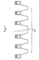
pad oxide 602 andportions 601A ofsubstrate 601 left uncovered by the resist 604 are etched. As shown in Figure 7, this etchingstep forms trenches 701 in the areas of the device left uncovered by the resist 604; - the resist 604 used in the above lithographic defining step is removed.
- The
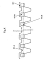
trenches 701 are filled with one or more dielectric material layers, obtained through oxidation or deposition. The aggregate of these dielectric material layers is commonly referred to as the field oxide and it is indicated withreference number 801 in Figure 8; - preferably, the
field oxide 801 is subjected to a thickening treatment to improve unevenness as for speed in etching the several layers forming it; - a planarising step is carried out, e.g. through CMP (Chemical-Mechanical
Polishing) technique. This planarising step, not illustrated,
is effective to reduce the height of the
field oxide 801 with respect to the surface of thesubstrate 601, levelling it down to that of aportion 603B of thenitride layer 603 still present. - The above planarising step may be followed by a wet etching step,
directed to further reduce the height of the
field oxide 801 with respect to the surface of thesubstrate 601. Afield oxide 801A, dot-lined in Figure 8, is thus obtained in some areas of the device, the field oxide having a lower height than that ofportion 603B of thenitride layer 603 still present, always with respect to the surface ofsubstrate 601. - Referring now to Figures 9A-9G, the following steps are carried out at this step of the inventive method, in sequential order:
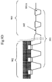
- a
matrix area 901 is lithographically defined as shown in Figure 9A by means of a mask using a resist 903, for example. This lithographic defining step is to protect acircuit area 902 during the next processing steps; - the left-over
portion 603B of thenitride layer 603 is removed from thematrix area 901, selectively with respect to thefield oxide 801A. This removal may occur for example by chemical attack with phosphoric acid (H3PO4); - left-over
portions 602B of thepad oxide layer 602 are removed from thematrix area 901 as shown in Figure 9C, for example through a BOE (Buffered Oxide Etch) etching or through a solution of diluted hydrofluoric acid (HF); - advantageously in this invention, the exposed portion of the
substrate 601 and of thefield oxide 801A are etched in thematrix area 901. In this embodiment, this etching realises a digging, which brings down the level of theactive areas 502 in thematrix area 901, preferably of equal thickness to that of the floating gate layer to be formed after. In the example, a digging of depth from approximately 50 to 200 nm, preferably from 80 to 130 nm. The formation of the digging is preferably performed in two subsequent steps, comprising a first step whereat the exposed portion of thesubstrate 601 is selectively etched to thefield oxide 801A, and a second etching step whereat thefield oxide 801A is etched. This field oxide 810A etching may be realised either through a BOE etching or through a diluted HF solution. Thus, in an advantageous way,differential isolation structures 501 are obtained by applying the method of the invention, these structures in the example here described are of the STI type and they are shown in Figure 9D. - The above resist 903 is then removed;
- a
sacrificial dielectric 905 is then grown in thematrix area 901 as shown in Figure 9E. In the here considered example of flow process, thesacrificial dielectric 905 is silicon oxide and it has the same thickness, ranging from 10 to 20 nm, as theportion 602C of thepad oxide 602 left over in thecircuit area 902. - The ion implanting steps needed to form the memory cells of the
matrix area 901 are performed through thesacrificial dielectric 905. These ion implanting steps are screened off in thecircuit area 902 by theportion 603B yet to be removed of thenitride layer 603; -
portion 603B of thenitride layer 603, left over in thecircuit area 902, is removed as shown in Figure 9F; - the
sacrificial dielectric 905 is removed from thematrix area 901. Advantageously, in the embodiment considered according to the invention, the left-overportion 602C ofpad oxide 602 in thecircuit area 902 is removed concurrently therewith, as shown in Figure 9G. - The here described example of flow process then continues with the customary steps of forming and defining dielectric material layers and electrically active layers on the
active areas 502 of thematrix area circuit area 902, shown in Figure 9G. The active devices, such as the transistors in thecircuit area 902 and the memory cells in thematrix area 901, would be completed next using conventional techniques. - The above described process steps of this invention provide, without further alterations of the flow process considered, a near-planar morphology at the level of definition of the gate regions for the device memory cells and transistors, as shown in Figure 5.
- This planar morphology, advantageously provided by the inventive method, makes the lithografic defining of the gate regions in the
circuit area 902 and thematrix area 901 easier to carry out in an optimum manner. - The inventive method just described affords two advantages, being independent one another, in a monolithically integrated semiconductor electronic device.
- On one side, this method provides differential isolation structures in areas requiring isolation structures of different thickness, without requiring repetition, with respect to a standard single-isolation flow process, of a series of steps such as lithographic defining of active areas, dielectric layers etching, silicon etching, and resist removal. Furthermore, with respect to a standard single-isolation flow process, this method provides differential isolation structures without using an additional mask that is needed in the prior art.
- So, in general, the method of this invention can be applied and it is advantageous whenever a monolithically integrated semiconductor electronic device is to be provided with isolation structures of different thickness in different areas, even when no floating gate layers are provided.
- The method of this invention is also effective to remove all current problems during lithographic defining of gate regions of memory cells and transistors, thereby overcoming the disadvantages of the prior art.
- These advantages are realised by introducing, in the construction of memory cells and transistors, an adequately different starting level with respect to a semiconductor material substrate. This feature advantageously overcomes the limitations of prior solutions to the aforementioned problems.
- In the light of the above considerations, the method of the invention may be applied and it is advantageous whenever planarity requires to be enhanced in the defining of one or more so-called pre-metal layers, that is layers formed over active areas before the electric contact and interconnection structures are formed. Thus, an aggregate of pre-metal layers is provided by this method with a planar overall morphology, which is obviously advantageous in terms of correct size of the concerned layers, thus leading to an improvement of the device performance.
- Furthermore, the structure according to this invention is highly advantageous also in the case of a monolithically integrated semiconductor electronic device, also not comprising floating-gate non-volatile memory cells, wherein areas involving the presence of different-thickness isolation structures and active devices with different heights with respect to a starting substrate are provided. In particular, the advantages of the inventive structure are to be appreciated when isolation structures of smaller thickness and active devices of greater height must be provided in one area with respect to another. In this case, in fact, the invention meets both requirements by a novel single structure.
Claims (27)
- A method for manufacturing differential isolation structures (501) in a monolithically integrated semiconductor electronic device, comprising a first step wherein active areas (502, 503) are defined on a semiconductor material substrate (601), a second step of forming isolation structures by realising trenches (701) in said substrate (601) and subsequent formation of field oxide (801A) in said trenches, and a third step of defining lithographically at least a first area (901) of the device, characterised in that it provides, in the above first area (901), a step of realisation of a digging in said field oxide (801A) and said substrate (601), before electrically active layers are formed and defined over said substrate (601), to obtain isolation structures having different thicknesses.
- A method according to Claim 1, characterised in that said digging is realised in two successive steps.
- A method according to Claim 2, characterised in that said two successive steps for realising said digging comprise a first step of selective etching of said substrate (601) towards said field oxide (801A), and a second step of etching of said field oxide (801A).
- A method according to Claim 3, characterised in that it provides a BOE etching during said second step of etching of said field oxide (801A).
- A method according to Claim 3, characterised in that it provides a diluted HF solution in said second step of etching of said field oxide (801A).
- A method according to Claim 1, comprising a subsequent step of forming a floating gate layer (507), characterised in that said digging has the same thickness as that of said floating gate layer (507).
- A method according to either Claim 1 or 6, characterised in that it realises said digging of a thickness comprised between 50 and 200 nm.
- A method according to either Claim 1 or 6, characterised in that it realises said digging of a thickness comprised between 80 and 130 nm.
- A method according to Claim 1, characterised in that it provides a step of forming a sacrificial dielectric (905) within said first device area (901).
- A method according to Claim 9, characterised in that said sacrificial dielectric has a thickness comprised between 10 and 20 nm.
- A method according to Claim 9, wherein a step of forming, on said substrate (601), a succession of one or more dielectric layers comprising a first silicon oxide layer (602) is provided before realising said digging, characterised in that said sacrificial dielectric (905) is silicon oxide and it has the same thickness as that of said first silicon oxide (602).
- A method according to Claim 11, wherein a step of removing said sacrificial dielectric (905) and a step of removing a portion (602C) of said first silicon oxide layer (602) are provided, characterised in that said removal of said sacrificial dielectric (905) and said removal of a portion (602C) of said first silicon oxide layer (602) are carried out simultaneously.
- A method according to Claim 9, characterised in that it also provides at least one step of implanting in said first device area (901) and of screening off said implanting step in at least a second device area (902) by means of a first nitride layer (603B).
- A monolithically integrated semiconductor electronic device structure, of the type containing at least a first area (901) and at least a second area (902), comprising a starting semiconductor material substrate (601), active areas (502, 503) and differential isolation structures (501), characterised in that said differential isolation structures (501) have a bottom wall (504) placed at the same depth with respect to the surface (205) of said starting substrate (601), said active areas (502, 503) of said first area (901) and said second area (902) are placed at a different depth with respect to the surface (205) of said starting substrate (601).
- A structure according to Claim 14, characterised in that said differential isolation structures (501) are of the STI type (hallow trench isolation) and they are filled with field oxide (801A).
- A structure according to either Claim 14 or 15, characterised in that said active areas (502) of said first area (901) are at a lower height with respect to said active areas (503) of said second area (902), as far as said bottom wall (504) of said differential isolation structures (501) are concerned.
- A structure according to either Claim 14 or 15, characterised in that a first plurality of electrically active pre-metal layers is provided above said active areas (502) of said first area (901), and that a second plurality of electrically active pre-metal layers is provided above said active areas (503) of said second area (902), said first plurality of electrically active pre-metal layers comprising a different number of electrically active pre-metal layers from said second plurality of electrically active pre-metal layers.
- A structure according to either Claim 14 or 15, characterised in that a first plurality of electrically active pre-metal layers is provided above said active areas (502) of said first area (901), and that a second plurality of electrically active pre-metal layers is provided above said active areas (503) of said second area (902), said first plurality of electrically active pre-metal layers having a different thickness from said second plurality of electrically active pre-metal layers.
- A structure according to either Claim 17 or 18, characterised in that the upper surface of said first plurality of electrically active pre-metal layers and the upper surface of said second plurality of electrically active pre-metal layers are at the same height with respect to said bottom wall (504) of said differential isolation structures (501).
- A structure according to Claim 16, characterised in that said active areas (502) of said first area (901) are memory cell active areas and said active areas (503) of said second area (902) are transistor active areas.
- A structure according to Claim 20, characterised in that said memory cell active areas (502) comprise a first dielectric layer (506) above said memory cell active areas (502), and comprise a second floating gate layer (507) formed above said first dielectric layer (506).
- A structure according to Claim 21, characterised in that the thickness of said second floating gate layer (507) equals the difference in height between said memory cell active areas (502) and said transistor active areas (503).
- A structure according to Claim 21, characterised in that said memory cell active areas (502) further comprise a third dielectric layer (508) above said second floating gate layer (507), the combined thickness of said second floating gate layer (507) and said third dielectric layer (508) being equal to the difference in height between said memory cell active areas (502) and said transistor active areas (503).
- A structure according to Claim 23, characterised in that said transistor active areas (503) comprise a fourth dielectric layer (509) above said transistor active areas (503), and that said memory cell active areas (502) and transistor active areas (503) further comprise a fifth layer (510) of an electrically active material above said first dielectric layer (506), said second floating gate layer (507), said third dielectric layer (508), and said fourth dielectric layer (509), the morphology of said fifth layer (510) of an electrically active material being near-planar.
- A structure according to Claim 24, characterised in that said fifth layer (510) of an electrically active material is a polysilicon layer.
- A structure according to either Claim 16 or 22 or 25, characterised in that the difference in height between said active areas (502) of said first area (901) and of said second area (902) is comprised between 50 and 200 nm.
- A structure according to either Claim 16 or 22 or 25, characterised in that the difference in height between said active areas (502) of said first area (901) and of said second area (902) is comprised between 80 and 130 nm.
Priority Applications (3)
| Application Number | Priority Date | Filing Date | Title |
|---|---|---|---|
| EP03425459A EP1496548B1 (en) | 2003-07-11 | 2003-07-11 | Method for manufacturing differential isolation structures in a semiconductor electronic device and corresponding structure |
| DE60318419T DE60318419T2 (en) | 2003-07-11 | 2003-07-11 | Method for producing different isolation structures in semiconductor devices and corresponding structure |
| US10/890,529 US7820504B2 (en) | 2003-07-11 | 2004-07-12 | Method for manufacturing differential isolation structures in a semiconductor electronic device and corresponding structure |
Applications Claiming Priority (1)
| Application Number | Priority Date | Filing Date | Title |
|---|---|---|---|
| EP03425459A EP1496548B1 (en) | 2003-07-11 | 2003-07-11 | Method for manufacturing differential isolation structures in a semiconductor electronic device and corresponding structure |
Publications (2)
| Publication Number | Publication Date |
|---|---|
| EP1496548A1 true EP1496548A1 (en) | 2005-01-12 |
| EP1496548B1 EP1496548B1 (en) | 2008-01-02 |
Family
ID=33442917
Family Applications (1)
| Application Number | Title | Priority Date | Filing Date |
|---|---|---|---|
| EP03425459A Expired - Lifetime EP1496548B1 (en) | 2003-07-11 | 2003-07-11 | Method for manufacturing differential isolation structures in a semiconductor electronic device and corresponding structure |
Country Status (3)
| Country | Link |
|---|---|
| US (1) | US7820504B2 (en) |
| EP (1) | EP1496548B1 (en) |
| DE (1) | DE60318419T2 (en) |
Families Citing this family (4)
| Publication number | Priority date | Publication date | Assignee | Title |
|---|---|---|---|---|
| JP5951213B2 (en) * | 2011-10-11 | 2016-07-13 | ルネサスエレクトロニクス株式会社 | Semiconductor device manufacturing method and semiconductor device |
| US9536888B2 (en) * | 2014-12-23 | 2017-01-03 | Taiwan Semiconductor Manufacturing Co., Ltd. | Method to prevent oxide damage and residue contamination for memory device |
| TWI691019B (en) * | 2019-03-19 | 2020-04-11 | 華邦電子股份有限公司 | Flash memory device and method for manufacturing the same |
| CN116156887B (en) * | 2021-11-22 | 2026-04-21 | 中芯北方集成电路制造(北京)有限公司 | A method for forming a planar flash memory device |
Citations (3)
| Publication number | Priority date | Publication date | Assignee | Title |
|---|---|---|---|---|
| US5889335A (en) * | 1997-09-09 | 1999-03-30 | Mitsubishi Denki Kabushiki Kaisha | Semiconductor device and method of manufacturing the same |
| US6181018B1 (en) * | 1998-06-12 | 2001-01-30 | Nec Corporation | Semiconductor device |
| US20020093071A1 (en) * | 2001-01-17 | 2002-07-18 | Chheda Sejal N. | Semiconductor tiling structure and method of formation |
Family Cites Families (6)
| Publication number | Priority date | Publication date | Assignee | Title |
|---|---|---|---|---|
| JPH07335883A (en) * | 1994-06-15 | 1995-12-22 | Toshiba Corp | Method for manufacturing semiconductor device |
| US6383861B1 (en) * | 1999-02-18 | 2002-05-07 | Micron Technology, Inc. | Method of fabricating a dual gate dielectric |
| JP2000349164A (en) * | 1999-06-08 | 2000-12-15 | Nec Corp | Method for manufacturing semiconductor device having element isolation insulating film |
| US6391720B1 (en) * | 2000-09-27 | 2002-05-21 | Chartered Semiconductor Manufacturing Ltd. | Process flow for a performance enhanced MOSFET with self-aligned, recessed channel |
| US6773999B2 (en) * | 2001-07-18 | 2004-08-10 | Matsushita Electric Industrial Co., Ltd. | Method for treating thick and thin gate insulating film with nitrogen plasma |
| US6835628B2 (en) * | 2001-11-05 | 2004-12-28 | Intersil Americas Inc. | Integrated circuit with a MOS capacitor |
-
2003
- 2003-07-11 DE DE60318419T patent/DE60318419T2/en not_active Expired - Lifetime
- 2003-07-11 EP EP03425459A patent/EP1496548B1/en not_active Expired - Lifetime
-
2004
- 2004-07-12 US US10/890,529 patent/US7820504B2/en not_active Expired - Lifetime
Patent Citations (3)
| Publication number | Priority date | Publication date | Assignee | Title |
|---|---|---|---|---|
| US5889335A (en) * | 1997-09-09 | 1999-03-30 | Mitsubishi Denki Kabushiki Kaisha | Semiconductor device and method of manufacturing the same |
| US6181018B1 (en) * | 1998-06-12 | 2001-01-30 | Nec Corporation | Semiconductor device |
| US20020093071A1 (en) * | 2001-01-17 | 2002-07-18 | Chheda Sejal N. | Semiconductor tiling structure and method of formation |
Also Published As
| Publication number | Publication date |
|---|---|
| US7820504B2 (en) | 2010-10-26 |
| DE60318419D1 (en) | 2008-02-14 |
| EP1496548B1 (en) | 2008-01-02 |
| US20050042812A1 (en) | 2005-02-24 |
| DE60318419T2 (en) | 2009-01-02 |
Similar Documents
| Publication | Publication Date | Title |
|---|---|---|
| US8343875B2 (en) | Methods of forming an integrated circuit with self-aligned trench formation | |
| US6949801B2 (en) | Dual trench isolation using single critical lithographic patterning | |
| US6436751B1 (en) | Fabrication method and structure of a flash memory | |
| US7151295B2 (en) | Non-volatile semiconductor memory device and process of manufacturing the same | |
| US20040061165A1 (en) | Floating gate memory fabrication methods comprising a field dielectric etch with a horizontal etch component | |
| US8647949B2 (en) | Structure and method of fabricating a transistor having a trench gate | |
| US6838342B1 (en) | Nonvolatile memory fabrication methods comprising lateral recessing of dielectric sidewalls at substrate isolation regions | |
| US7585724B2 (en) | FLASH memory device and method of manufacture | |
| US7977191B2 (en) | Method for fabricating flash memory device | |
| US7943478B2 (en) | Semiconductor device manufacturing method | |
| EP1496548B1 (en) | Method for manufacturing differential isolation structures in a semiconductor electronic device and corresponding structure | |
| CN100546016C (en) | Method for manufacturing semiconductor device | |
| US7094644B2 (en) | Method for manufacturing a semiconductor device | |
| US20080093655A1 (en) | Semiconductor device and method for forming the same | |
| KR100875079B1 (en) | Manufacturing Method of Flash Memory Device | |
| US20030100166A1 (en) | Method for avoiding the effects of lack of uniformity in trench isolated integrated circuits | |
| JP2008004881A (en) | Method for manufacturing element isolation structure | |
| US20080299722A1 (en) | Manufacturing method for forming a recessed channel transistor, method for forming a corresponding integrated semiconductor memory device and corresponding self-aligned mask structure | |
| US20070262476A1 (en) | Method for providing STI structures with high coupling ratio in integrated circuit manufacturing | |
| EP1770772B1 (en) | Process for manufacturing a non-volatile memory device | |
| KR20070002293A (en) | Manufacturing Method of Flash Memory Device | |
| KR20060066874A (en) | Manufacturing Method of Flash Memory Device | |
| KR20080060553A (en) | Manufacturing method of nonvolatile memory device |
Legal Events
| Date | Code | Title | Description |
|---|---|---|---|
| PUAI | Public reference made under article 153(3) epc to a published international application that has entered the european phase |
Free format text: ORIGINAL CODE: 0009012 |
|
| AK | Designated contracting states |
Kind code of ref document: A1 Designated state(s): AT BE BG CH CY CZ DE DK EE ES FI FR GB GR HU IE IT LI LU MC NL PT RO SE SI SK TR |
|
| AX | Request for extension of the european patent |
Extension state: AL LT LV MK |
|
| 17P | Request for examination filed |
Effective date: 20050630 |
|
| AKX | Designation fees paid |
Designated state(s): DE FR GB IT |
|
| GRAP | Despatch of communication of intention to grant a patent |
Free format text: ORIGINAL CODE: EPIDOSNIGR1 |
|
| GRAS | Grant fee paid |
Free format text: ORIGINAL CODE: EPIDOSNIGR3 |
|
| GRAA | (expected) grant |
Free format text: ORIGINAL CODE: 0009210 |
|
| AK | Designated contracting states |
Kind code of ref document: B1 Designated state(s): DE FR GB IT |
|
| REG | Reference to a national code |
Ref country code: GB Ref legal event code: FG4D |
|
| REF | Corresponds to: |
Ref document number: 60318419 Country of ref document: DE Date of ref document: 20080214 Kind code of ref document: P |
|
| REG | Reference to a national code |
Ref country code: DE Ref legal event code: R096 Ref document number: 60318419 Country of ref document: DE Effective date: 20080214 |
|
| ET | Fr: translation filed | ||
| PLBE | No opposition filed within time limit |
Free format text: ORIGINAL CODE: 0009261 |
|
| STAA | Information on the status of an ep patent application or granted ep patent |
Free format text: STATUS: NO OPPOSITION FILED WITHIN TIME LIMIT |
|
| PGFP | Annual fee paid to national office [announced via postgrant information from national office to epo] |
Ref country code: FR Payment date: 20080730 Year of fee payment: 6 |
|
| 26N | No opposition filed |
Effective date: 20081003 |
|
| REG | Reference to a national code |
Ref country code: DE Ref legal event code: R097 Ref document number: 60318419 Country of ref document: DE Effective date: 20081002 |
|
| GBPC | Gb: european patent ceased through non-payment of renewal fee |
Effective date: 20080711 |
|
| PG25 | Lapsed in a contracting state [announced via postgrant information from national office to epo] |
Ref country code: GB Free format text: LAPSE BECAUSE OF NON-PAYMENT OF DUE FEES Effective date: 20080711 |
|
| PG25 | Lapsed in a contracting state [announced via postgrant information from national office to epo] |
Ref country code: IT Free format text: LAPSE BECAUSE OF FAILURE TO SUBMIT A TRANSLATION OF THE DESCRIPTION OR TO PAY THE FEE WITHIN THE PRESCRIBED TIME-LIMIT Effective date: 20080102 |
|
| REG | Reference to a national code |
Ref country code: FR Ref legal event code: ST Effective date: 20100331 |
|
| PG25 | Lapsed in a contracting state [announced via postgrant information from national office to epo] |
Ref country code: FR Free format text: LAPSE BECAUSE OF NON-PAYMENT OF DUE FEES Effective date: 20090731 |
|
| REG | Reference to a national code |
Ref country code: DE Ref legal event code: R082 Ref document number: 60318419 Country of ref document: DE Representative=s name: SAMSON & PARTNER, PATENTANWAELTE, DE |
|
| REG | Reference to a national code |
Ref country code: DE Ref legal event code: R081 Ref document number: 60318419 Country of ref document: DE Owner name: MICRON TECHNOLOGY, INC., BOISE, US Free format text: FORMER OWNER: STMICROELECTRONICS S.R.L., AGRATE BRIANZA, MAILAND/MILANO, IT Effective date: 20130708 Ref country code: DE Ref legal event code: R082 Ref document number: 60318419 Country of ref document: DE Representative=s name: SAMSON & PARTNER PATENTANWAELTE MBB, DE Effective date: 20130708 Ref country code: DE Ref legal event code: R081 Ref document number: 60318419 Country of ref document: DE Owner name: MICRON TECHNOLOGY, INC., BOISE, US Free format text: FORMER OWNER: STMICROELECTRONICS S.R.L., AGRATE BRIANZA, IT Effective date: 20130708 Ref country code: DE Ref legal event code: R081 Ref document number: 60318419 Country of ref document: DE Owner name: MICRON TECHNOLOGY, INC., US Free format text: FORMER OWNER: STMICROELECTRONICS S.R.L., AGRATE BRIANZA, IT Effective date: 20130708 Ref country code: DE Ref legal event code: R082 Ref document number: 60318419 Country of ref document: DE Representative=s name: SAMSON & PARTNER, PATENTANWAELTE, DE Effective date: 20130708 |
|
| PGFP | Annual fee paid to national office [announced via postgrant information from national office to epo] |
Ref country code: DE Payment date: 20220527 Year of fee payment: 20 |
|
| REG | Reference to a national code |
Ref country code: DE Ref legal event code: R071 Ref document number: 60318419 Country of ref document: DE |