EP1496436B1 - Method and apparatus for autoreset of a usb smart card device in a mute mode - Google Patents
Method and apparatus for autoreset of a usb smart card device in a mute mode Download PDFInfo
- Publication number
- EP1496436B1 EP1496436B1 EP04254046.8A EP04254046A EP1496436B1 EP 1496436 B1 EP1496436 B1 EP 1496436B1 EP 04254046 A EP04254046 A EP 04254046A EP 1496436 B1 EP1496436 B1 EP 1496436B1
- Authority
- EP
- European Patent Office
- Prior art keywords
- processor
- control logic
- status register
- mute mode
- status
- Prior art date
- Legal status (The legal status is an assumption and is not a legal conclusion. Google has not performed a legal analysis and makes no representation as to the accuracy of the status listed.)
- Active
Links
- 238000000034 method Methods 0.000 title claims description 15
- 238000004891 communication Methods 0.000 claims description 11
- 230000007704 transition Effects 0.000 claims description 8
- 230000004044 response Effects 0.000 claims description 5
- 230000000977 initiatory effect Effects 0.000 claims description 3
- 238000010586 diagram Methods 0.000 description 12
- 230000002093 peripheral effect Effects 0.000 description 7
- 230000009471 action Effects 0.000 description 4
- 230000008859 change Effects 0.000 description 4
- 230000015654 memory Effects 0.000 description 4
- 230000004048 modification Effects 0.000 description 4
- 238000012986 modification Methods 0.000 description 4
- 230000002159 abnormal effect Effects 0.000 description 3
- 230000008901 benefit Effects 0.000 description 3
- 238000012546 transfer Methods 0.000 description 3
- 230000003993 interaction Effects 0.000 description 2
- 239000000463 material Substances 0.000 description 2
- 238000012545 processing Methods 0.000 description 2
- 230000003139 buffering effect Effects 0.000 description 1
- 238000013461 design Methods 0.000 description 1
- 238000001514 detection method Methods 0.000 description 1
- 230000006870 function Effects 0.000 description 1
- 230000007257 malfunction Effects 0.000 description 1
- 230000007246 mechanism Effects 0.000 description 1
- 230000008520 organization Effects 0.000 description 1
Images


Classifications
-
- G—PHYSICS
- G06—COMPUTING; CALCULATING OR COUNTING
- G06F—ELECTRIC DIGITAL DATA PROCESSING
- G06F1/00—Details not covered by groups G06F3/00 - G06F13/00 and G06F21/00
- G06F1/24—Resetting means
-
- G—PHYSICS
- G06—COMPUTING; CALCULATING OR COUNTING
- G06F—ELECTRIC DIGITAL DATA PROCESSING
- G06F11/00—Error detection; Error correction; Monitoring
- G06F11/07—Responding to the occurrence of a fault, e.g. fault tolerance
- G06F11/0703—Error or fault processing not based on redundancy, i.e. by taking additional measures to deal with the error or fault not making use of redundancy in operation, in hardware, or in data representation
- G06F11/0706—Error or fault processing not based on redundancy, i.e. by taking additional measures to deal with the error or fault not making use of redundancy in operation, in hardware, or in data representation the processing taking place on a specific hardware platform or in a specific software environment
- G06F11/0745—Error or fault processing not based on redundancy, i.e. by taking additional measures to deal with the error or fault not making use of redundancy in operation, in hardware, or in data representation the processing taking place on a specific hardware platform or in a specific software environment in an input/output transactions management context
-
- G—PHYSICS
- G06—COMPUTING; CALCULATING OR COUNTING
- G06F—ELECTRIC DIGITAL DATA PROCESSING
- G06F11/00—Error detection; Error correction; Monitoring
- G06F11/07—Responding to the occurrence of a fault, e.g. fault tolerance
- G06F11/0703—Error or fault processing not based on redundancy, i.e. by taking additional measures to deal with the error or fault not making use of redundancy in operation, in hardware, or in data representation
- G06F11/0793—Remedial or corrective actions
-
- G—PHYSICS
- G06—COMPUTING; CALCULATING OR COUNTING
- G06F—ELECTRIC DIGITAL DATA PROCESSING
- G06F11/00—Error detection; Error correction; Monitoring
- G06F11/07—Responding to the occurrence of a fault, e.g. fault tolerance
- G06F11/14—Error detection or correction of the data by redundancy in operation
- G06F11/1402—Saving, restoring, recovering or retrying
- G06F11/1415—Saving, restoring, recovering or retrying at system level
- G06F11/1441—Resetting or repowering
Definitions
- the present disclosure relates generally to smart card systems, and in particular but not exclusively, relates to automatically resetting a smart card (SC) device that has entered a mute mode.
- SC smart card
- Smart cards are plastic cards having an embedded integrated circuit (IC). That IC may be a logic circuit with its associated memories, a microcontroller or microprocessor with its associated memories and software, or other type of intelligence.
- IC integrated circuit
- the IC of an SC is typically coupled to contact pads, which allow the SC to communicate or perform transactions with external devices using some type of protocol.
- external devices can include an SC reader, a host personal computer (PC), SC adapters and connectors, and the like.
- SC adapters and connectors can include an SC reader, a host personal computer (PC), SC adapters and connectors, and the like.
- SC adapters and connectors can include an SC reader, a host personal computer (PC), SC adapters and connectors, and the like.
- SCs that are available.
- the mechanical and electrical specifications of SCs are published by the International Standard Organization (ISO). For instance, the ISO 7816 protocol supports contact modes for SCs, while the ISO 14443 protocol supports contactless modes for SCs.
- ISO International Standard Organization
- USB Universal Serial Bus
- a USB smart card sometimes goes into a "mute” state or “mute” mode.
- This is a state that the SC enters when it has detected a malfunction or other abnormal condition in its operation.
- the abnormal condition can include, but not be limited to, a change in the SC's embedded code, a hacker attack, receipt of an unauthorized command, and the like.
- the SC no longer responds to further commands, and more particularly, the central processing unit (CPU) or other processor of the SC does not respond to any commands or requests presented on the USB port to which it is coupled.
- CPU central processing unit
- One technique to remove the SC from the mute mode is to perform a "hard reset" on the SC (i.e. , turn the power supplied to the SC's bus off and then turn the power back on) and start over.
- a bus reset i.e. , turn the power supplied to the SC's bus off and then turn the power back on
- USB implementations if such a bus reset is used to reset the SC's CPU, the enumeration, configuration, etc. of the SC on the bus is lost.
- Some SC applications cannot accept the lost of such data.
- WO 97/24652 describes a rest circuit for an integrated circuit.
- a watchdog timer outputs a signal if a processor fails to write to the watchdog timer.
- the processor is reset in response to this.
- US 6,439,464 describes a dual-mode integrated circuit for a smart card that can swap between a USB and ISO mode.
- a smart card apparatus comprising: a processor; a status register coupled to the processor to store status information indicative of a status associated with the processor characterized in that the processor writes to the status register to indicate transition of the processor to a mute mode just before the processor enters a mute mode; the smart card apparatus further comprising a device controller that can perform register-based and interrupt-based communication with the processor, the device controller including: control logic coupled to the processor and to the status register to check the status information stored therein to determine the status of the processor, wherein if the control logic determines that the status information indicates a mute mode associated with the processor, the control logic can initiate an interrupt-based reset signal to the processor to remove the processor from the mute mode and the device controller maintains a current configuration and state of the device controller.
- a smart card system comprising: the smart apparatus of the first aspect; a means for providing external information to the processor and for receiving information from the processor; a means for communicating between the means for providing external information and the processor; a means for receiving the external information from the means for communicating; and a means for routing and for buffering the received external information.
- a method usable for a smart card comprising: writing to a status register to indicate the transition of a processor to a mute mode just before the processor enters a mute mode; storing status information indicative of a status associated with the processor in the status register; checking the stored status information to determine the status of the processor; and if the status information indicates a mute mode associated with the processor, initiating an interrupt-based reset signal to the processor to remove the processor from the mute mode; wherein checking the stored status information and initiating a reset signal is carried out by a device controller that can perform register-based and interrupt-based communication with the processor and the current configuration and state of the device controller is maintained when the reset signal is initiated
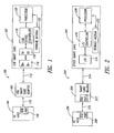
- Figure 1 is a block diagram illustrating a system in which one embodiment of the invention may be implemented.
- FIG. 2 is a block diagram illustrating another system in which one aspect of the invention may be implemented.
- FIG. 3 is a block diagram illustrating components of a SC in accordance with an embodiment of the invention.
- Figure 4 is a block diagram illustrating operation of the components of Figure 3 in more detail in accordance with an embodiment of the invention.
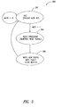
- FIG. 5 is a state diagram of control logic that can be implemented by the component(s) of Figures 3-4 in accordance with an embodiment of the invention.
- an embodiment of the invention provides a technique to automatically get a SC out of a mode where the SC is no longer accepting or processing commands. More particularly in one embodiment, a technique is provided to autoreset a USB SC from a mute mode.
- autoreset may be performed without having to create or define a specific USB vendor specific request (VSR) that generates a "warm reset” (i . e ., a software reset command from the USB host).
- VSR is a functionality provided by the USB specification that allows the user to define application functions in the control transfer mode that are not included in the USB specification.
- DoReset a specifically defined VSR
- the VSR is decoded by the hardware of the SC in the USB device controller and generates a hardware “warm reset” within the SC.
- a “warm reset” is different from a “cold reset,” which is the hardware reset of a device.
- Usually a "warm reset” is generated by software.
- a particularity of this "warm reset" in this embodiment is to reset only the processor and not the USB device controller.
- a VSR implementation is typically more inflexible and complex, since it often needs a specific PC driver to be loaded onto the PC host and/or SC. Moreover, such specific VSRs would require hardware modification of a SC, with the VSR having to be decoded by the hardware and the control logic has to manage its action, which may undesirably take a SC out of a standard device class.
- an embodiment of the invention provides a USB device controller (on the SC) that detects the state of the SC's CPU by polling a status register, and in the event of a mute mode, the USB device controller automatically generates a reset of the SC's CPU, thereby preserving the USB device controller configuration and setting and thus maintaining the communication with the USB host.
- a USB smart card comprises a microcontroller (such as a CPU or other processor) and a USB peripheral block on the same chip.
- the USB peripheral block is a slave to an external USB host, and is designed to respond to all standard USB or VSR requests from the USB host.
- the USB host uses a command (such as Control Mode Transfer) to control or send specific commands to a USB SC.
- a command such as Control Mode Transfer
- the USB specification has some features to ensure that the USB bus is always ready, such as Bus Reset, Single-Ended Zero (SE0), Suspend and Resume, Keep Alive, Preamble, etc.
- the role of the USB peripheral block is to then transfer data received from the USB host to the SC's CPU and memories, and vice-versa.
- the SC's CPU decodes the data, which can be a higher-level instruction or request from the host PC, or simply reads such data so that it can be used by some embedded application(s).
- the interaction between the microcontroller and the USB peripheral block requires that they always be in operation.
- the SC's CPU stops responding to requests from the USB peripheral block, which causes the USB peripheral block to stall or otherwise not respond to the USB host's requests.
- the SC has thus entered a mute mode, where as described above, a hard reset may be performed to remove the SC from the mute mode.
- a hard reset may be performed to remove the SC from the mute mode.
- another technique is to use a VSR, if one has been defined, to perform a warm reset.
- alternative or additional techniques are provided to automatically perform the reset.
- the USB smart card apparatus includes a processor and a USB device controller.
- the communication between these two entities is register-based coupled with an interrupt-based mechanism in an embodiment.
- This register interface includes a status register coupled to the processor to store status information indicative of a status associated with the processor.
- Control logic which is part of the USB device controller, is coupled to the processor and to the status register to check the status information stored therein to determine the status of the processor. If the control logic determines that the status information indicates a non-responsive state associated with the processor, the control logic can initiate an interrupt-based reset signal to the processor to remove the processor from the non-responsive state. This reset is done keeping current the configuration and state of the USB device controller.
- FIG. 1 is a block diagram illustrating a system 100 in which one embodiment of the invention may be implemented.
- a USB smart card 102 is communicatively coupled to a PC host 104 by way of a USB smart card adapter 106.
- the PC host 104 includes a USB port 108, which is used to communicatively couple the PC host 104 to the USB smart card adapter 106 via a connection 110 (such as a USB serial cable).
- a connection 112 completes the serial connection between the USB SC 102 and the PC host 104.
- Suitable USB smart card adapters are available in Schlumberger's line of E-gate smart card products, for example.
- An embodiment of the SC 102 includes D+ and D- pads 114 for communication in accordance with the USB specification, a transceiver 116 to transmit and receive information between the PC host 104 and the SC 102, a USB device controller 118, a processor 120 (such as a microcontroller, CPU, or other type of processor), and a storage medium 122 with which either one or both the processor 120 or the USB device controller 118 can communicate.
- a smart card having the autoreset features described herein may be also implemented in multi-mode smart cards, such as the USB-ISO dual-mode smart card disclosed in U.S. Patent No. 6,439,464 , which is incorporated herein by reference.
- one embodiment of the USB device controller 118 is coupled to determine the state of the processor 120 (e.g. , whether the processor 120 has entered a mute mode), such as by checking one or more status registers that is written to by the processor 120 before going to mute mode, and then takes the appropriate action to automatically reset the processor 120 from the mute mode.
- the status register(s) may comprise part of the USB device controller 118 or part of the storage medium 122.
- the storage medium 122 can itself comprise one or more machine-readable storage locations to store this status information, embedded software or code, data exchanged or to be exchanged between the SC 102 and the host PC 104, or other machine-readable instruction, data, or code.
- the storage medium 122 can be embodied as a cache, buffer, read only memory (ROM), random access memory, data register, or other suitable data repository.
- FIG 2 is a block diagram illustrating another system 200 for comparison with the system 100 of Figure 1 . More specifically, some other type (e . g ., such as an ISO 7816 smart card) smart card 202 is provided.
- the SC 202 communicates with a PC host 204 by way of a smart card reader 206.
- the PC host 204 may be a USB host that communicates with the smart card reader 206 by way of a connection 210 (such as a USB serial cable) between their USB ports 209 and 212.
- a connection 214 can comprise an ISO 7816 contact interface.
- the SC 202 includes an input/output (I/O) controller 218, a processor 220, and a storage medium 222.
- the I/O controller 218 is compliant with the ISO 7816-3 protocol, for instance.
- the SC 202 includes an I/O block 216, such as those used in an ISO 7816-compliant smart card.
- FIG. 3 is a block diagram illustrating components of a SC in accordance with an embodiment of the invention. More specifically, Figure 3 shows components of the USB device controller 118 of the SC 102 in more detail.
- the USB device controller 118 includes a serial interface engine 300 through which is routed information to be sent to the PC host 104 or received from the PC host 104.
- the serial interface engine 300 receives serial data from the transceiver 116 and parallelizes the data.
- a buffer 302 is coupled between the serial interface engine 300 and the processor 302 to store this and other information, if necessary, as the information is transferred between the processor 120 and the PC host 104.
- Control logic 304 is coupled to the buffer 302 and to the serial interface engine 300 to manage and control the flow of information between the buffer 302 and the processor 120, and to also receive (or send) data (such as the parallelized data) from the serial interface engine 302 as appropriate, so that the control logic 304 can decode this data or perform other operations related to the data.
- the communication between the USB device controller 118 and the processor 120 can be interrupt-based in an embodiment.
- control logic 304 is coupled to determine the state or mode of the processor 120 and to reset it if necessary.
- the processor 120 repeatedly writes its status information into a status register 306.
- the control logic 304 polls this status register 306, and if it detects a mute mode (such as if a bit or flag is set to binary 1), the control logic 304 initiates a reset command to the processor 120 via a reset block 308.
- the buffer 302 and the status register 306 have been indicated as comprising part of the USB device controller 118. Again, it is appreciated that such components may be separately located elsewhere on the SC 102, such as in the storage medium 122, in other embodiments.
- Figure 4 is a block diagram illustrating operation of the components of Figure 3 in more detail in accordance with an embodiment of the invention. More particularly, Figure 4 illustrates the relative interaction and connection of some of the USB device controller 118 components in more detail, and the manner in which the processor 120 may be reset. Figure 4 depicts at least three possible types of actions that may be used to reset the processor 120: a hard reset, a warm reset via use of a VSR, and an autoreset in accordance with an embodiment of the invention. The autoreset action may be used alone or in combination with either one or both the warm reset of the VSR and the hard reset.
- a hard reset e . g ., turning the power to the USB SC bus off or on, such as when initially powering up the SC 102 or when "rebooting” it
- a Power On Reset (POR) circuit 400 supplies V BUS (which may be between 4 volts and 5.5 volts supplied via the USB bus, for example) to the processor 120 to power the processor 120.
- V BUS is cut off from the processor 120 by the POR circuit 400 during the hard reset, and then subsequently re-supplied to the processor 120.
- the reset block 308 comprises an OR gate as depicted in Figure 4 , having a first input terminal 402 coupled to an output terminal of the POR circuit 400.
- the POR circuit 400 provides a binary 1 (or other suitable input signal) on the first input terminal 402 of the OR gate, for instance.
- the OR gate has an output terminal 406 coupled to the processor 120 to provide a RESET signal thereto.
- a second input terminal 404 of the OR gate is coupled to an output terminal of the control logic 304.
- the control logic 304 provides a binary 1, for example, on the second input terminal 404 of the OR gate if either one or both the warm reset of the VSR and the autoreset of an embodiment requires a reset of the processor 120.
- a VSR block 408 is provided to receive the reset VSR (such as a DoReset command) from the D+ and D- pads 114 by way of the transceiver 116, if such a VSR has been defined and has been communicated by the PC host 104 to the SC 102.
- the VSR block 408 is a circuit that decodes this VSR (as well as other VSRs that may be received), and to generate an output therefrom that instructs the control logic 304 to reset the processor 120.
- the control logic 304 can do at least some of the decoding.
- This output from the VSR block 408 (a binary 1, for example) is provided from an output terminal of the VSR block 408 to a first input terminal 410 of the control logic 304.
- the control logic 304 Upon receipt of this output from the VSR block 410, the control logic 304 provides a binary 1, for example, to the second input terminal 404 of the OR gate, which in response provides the RESET signal on its output terminal 406 to reset the processor 120.
- an embodiment of the invention provides use of the status register 306. This technique allows a reset to be automatically performed within the SC 102 itself, without needing the PC host 104 to generate a specific VSR command. Thus, when a mute mode is entered where the SC 102 stops responding to commands from the PC host 104, the communication link between the PC host 104 need not broken ⁇ the SC 102 can internally initiate a reset of the processor 120 and thereby resume communication with the PC host after reset.
- the processor 120 writes its status to the status register 306 via a WRITE line.
- the processor 120 may regularly write to a bit of the status register 306 to indicate that it is ready, busy, mute, or other status information that indicates the status of the communication link between the processor 120 and the USB device controller 118. This writing to indicate transition to a mute mode may be performed in a number of possible ways.
- the processor 120 may write (via the WRITE line) to a mute bit in the status register 306 to set that bit high to a binary 1.
- the WRITE line may comprise an enable line to enable a corresponding mute bit or other element in the status register 306 that indicates the mute mode of the processor 120. It is appreciated that instead of setting the bit high to a binary 1 or using an enable line, a mute mode may be indicated by setting a bit low to a binary 0 or by using a disable line.
- the control logic 304 polls the status register 306 to determine the status of the processor 120 and to receive the status information at its second input terminal 412. In an embodiment, this polling may be performed at suitable time intervals that are sufficiently spaced in time to be able to detect a change from one state to another, while in another embodiment and instead of polling, the status register 306 may provide updated status information to input terminal 412 of the control logic 304 only when there is a status change, for example.
- control logic 304 If the status information received by the control logic 304 at its second input terminal 412 indicates a mute mode, then the control logic 304 generates a binary 1 output, for example, for the second input terminal 404 of the OR gate, which then generates the RESET signal at its output terminal 406 to reset the processor 120. The control logic 304 then provides a signal on a RESET STATUS line that writes to the status register 306, to indicate the new status of the processor 120 (e.g. , ready, busy, or other status to indicate that the processor 120 has been taken off the mute mode).
- a RESET STATUS line that writes to the status register 306, to indicate the new status of the processor 120 (e.g. , ready, busy, or other status to indicate that the processor 120 has been taken off the mute mode).
- the status register 306 has two bits: mute bit and mute flag bit.
- the mute bit is written to by the processor 120 on the WRITE line to indicate its status, and is cleared by the control logic 304 via a CLEAR line (such as after the processor 120 has been reset from the mute mode).
- the mute flag bit is a history bit indicating that the processor 120 was in mute mode and is reset by the control logic 304.
- the mute flag bit serves as a history bit that keeps track of the previous mute state--this information can be used by the processor 120 to count the number of times that the processor 120 went through a mute mode, and thus help the processor decide to not reset after a certain number of times, three times for example.
- Figure 5 is a state diagram 500 of the control logic 304 that can be implemented by the component(s) shown in Figures 3-4 in accordance with an embodiment of the invention.
- a person skilled in the art having the benefit of this disclosure can design the suitable hardware logic that will operate in accordance with the state diagram 500.
- the operations depicted in the state diagram 500 and described with respect to the other figures can be implemented in software or other machine-readable instruction stored on the machine-readable storage medium 122.
- the control logic 304 (as a state machine in one embodiment) repeatedly polls the mute bit (or flag) in the status register 306. If the processor 120 has not entered into the mute mode, then the mute bit has a value of binary 0, for example. If the processor 120 is about to enter the mute mode, then the processor 120 writes to the status register 306 to set the mute bit to a value of binary 1, for example.
- the mute bit at binary 1 causes the control logic 504 to transition to a state 504, where it initiates a reset of the processor 120. As depicted by way of example in Figure 4 , the control logic 504 initiates this reset by providing a signal to the OR gate, which then generates the RESET signal at its output terminal 406 and provides the RESET signal to the processor 120.
- the control logic 304 transitions to a state 506.
- the control logic 304 writes the new status of the processor 120 in the status register 306.
- the mute flag bit is set to binary 1 to keep the track of the previous mute state.
- the mute bit is cleared (to binary 0, for instance, or other reset status) to be able to catch the next mute state of the processor 120.
- the state of the control logic 304 returns to the state 502, where the mute bit is again repeatedly polled for processor status information.
- an aspect of the invention allows a USB SC or other type of SC to be taken out of a mute or other similar mode without necessarily having to define and use a VSR.
- This feature allows such SCs to be used for USB devices classes that allow "plug 'n play" and that are directly recognized by standard operating systems, without having to load a specific driver.
- One of many examples of such a USB class is the Chip Card Interface Device (CCID) class.
- CCID Chip Card Interface Device
- USB device controller 118 One advantage of this solution compared to previous systems based on an ISO smart card is the intelligence in the USB device controller 118. Contrary to an ISO smart card's I/O controller 218 that basically sets the direction and the interrupt of the I/O block 216, the USB device controller 118 has its own logic state machine dedicated to the USB protocol and the communication with the CPU. Because of this intelligence, there are other choices to get a CPU of a USB smart card out of the Mute mode, than having the host PC 104 or the reader software execute a special command.
- a USB smart card comprises not a single controller but two controllers on the same chip: the processor 120 (e.g. , a CPU) and the USB device controller 118.
- the processor 120 e.g. , a CPU
- the USB device controller 118 This is different than an ISO 7816-3 smart card that has only one controller: the CPU. Therefore, one embodiment of the solution to reset a USB smart card in mute mode can be done by the USB host firmware in a similar manner as the firmware of a ISO 7816-3 smart card reader for a ISO smart card, or directly by the USB device controller 118, which is sufficiently intelligent to perform the reset upon the detection of a mute condition.
- USB Universal Serial Bus
- the invention is not necessarily limited to this.
- Other aspects of the invention can have implementations based on other standards, protocols, or configurations that operate in a manner similar to USB.
Description
- The present disclosure relates generally to smart card systems, and in particular but not exclusively, relates to automatically resetting a smart card (SC) device that has entered a mute mode.
- Smart cards are plastic cards having an embedded integrated circuit (IC). That IC may be a logic circuit with its associated memories, a microcontroller or microprocessor with its associated memories and software, or other type of intelligence.
- The IC of an SC is typically coupled to contact pads, which allow the SC to communicate or perform transactions with external devices using some type of protocol. These external devices can include an SC reader, a host personal computer (PC), SC adapters and connectors, and the like. There are also "contactless" SCs that are available.
- The mechanical and electrical specifications of SCs are published by the International Standard Organization (ISO). For instance, the ISO 7816 protocol supports contact modes for SCs, while the ISO 14443 protocol supports contactless modes for SCs.
- The Universal Serial Bus (USB) standard has become firmly established and has gained wide acceptance in the PC marketplace. The USB standard was developed in response to a need for a standard interface that extends the concept of "plug and play" to devices external to a PC. It has enabled users to install and remove peripheral devices external to the PC without having to open the PC case or to remove power from the PC (e.g., without having to "reboot"). The USB standard provides a low-cost, high-performance serial interface that is easy to use and readily expandable, and is supported by an increasing number of SCs that are available in the marketplace.
- A USB smart card sometimes goes into a "mute" state or "mute" mode. This is a state that the SC enters when it has detected a malfunction or other abnormal condition in its operation. The abnormal condition can include, but not be limited to, a change in the SC's embedded code, a hacker attack, receipt of an unauthorized command, and the like. In the mute mode, the SC no longer responds to further commands, and more particularly, the central processing unit (CPU) or other processor of the SC does not respond to any commands or requests presented on the USB port to which it is coupled.
- One technique to remove the SC from the mute mode is to perform a "hard reset" on the SC (i.e., turn the power supplied to the SC's bus off and then turn the power back on) and start over. However, with USB implementations, if such a bus reset is used to reset the SC's CPU, the enumeration, configuration, etc. of the SC on the bus is lost. Some SC applications cannot accept the lost of such data.
-
WO 97/24652 -
US 6,439,464 describes a dual-mode integrated circuit for a smart card that can swap between a USB and ISO mode. - According to a first aspect of the present invention there is provided a smart card apparatus, comprising: a processor; a status register coupled to the processor to store status information indicative of a status associated with the processor characterized in that the processor writes to the status register to indicate transition of the processor to a mute mode just before the processor enters a mute mode; the smart card apparatus further comprising a device controller that can perform register-based and interrupt-based communication with the processor, the device controller including: control logic coupled to the processor and to the status register to check the status information stored therein to determine the status of the processor, wherein if the control logic determines that the status information indicates a mute mode associated with the processor, the control logic can initiate an interrupt-based reset signal to the processor to remove the processor from the mute mode and the device controller maintains a current configuration and state of the device controller.
- According to a second aspect there is provided a smart card system, comprising: the smart apparatus of the first aspect; a means for providing external information to the processor and for receiving information from the processor; a means for communicating between the means for providing external information and the processor; a means for receiving the external information from the means for communicating; and a means for routing and for buffering the received external information.
- According to a third aspect there is provided a method usable for a smart card, the method comprising: writing to a status register to indicate the transition of a processor to a mute mode just before the processor enters a mute mode; storing status information indicative of a status associated with the processor in the status register; checking the stored status information to determine the status of the processor; and if the status information indicates a mute mode associated with the processor, initiating an interrupt-based reset signal to the processor to remove the processor from the mute mode; wherein checking the stored status information and initiating a reset signal is carried out by a device controller that can perform register-based and interrupt-based communication with the processor and the current configuration and state of the device controller is maintained when the reset signal is initiated
- Non-limiting and non-exhaustive embodiments of the present invention are described with reference to the following figures, wherein like reference numerals refer to like parts throughout the various views unless otherwise specified.
-
Figure 1 is a block diagram illustrating a system in which one embodiment of the invention may be implemented. -
Figure 2 is a block diagram illustrating another system in which one aspect of the invention may be implemented. -
Figure 3 is a block diagram illustrating components of a SC in accordance with an embodiment of the invention. -
Figure 4 is a block diagram illustrating operation of the components ofFigure 3 in more detail in accordance with an embodiment of the invention. -
Figure 5 is a state diagram of control logic that can be implemented by the component(s) ofFigures 3-4 in accordance with an embodiment of the invention. - Embodiments for autoreset of smart card devices, such as a Universal Serial Bus (USB) smart card, in a mute mode (or other similar mode) are described herein. In the following description, numerous specific details are given to provide a thorough understanding of embodiments of the invention. One skilled in the relevant art will recognize, however, that the invention can be practiced without one or more of the specific details, or with other methods, components, materials, etc. In other instances, well-known structures, materials, or operations are not shown or described in detail to avoid obscuring aspects of the invention.
- Reference throughout this specification to "one embodiment" or "an embodiment" means that a particular feature, structure, or characteristic described in connection with the embodiment is included in at least one embodiment of the present invention. Thus, the appearances of the phrases "in one embodiment" or "in an embodiment" in various places throughout this specification are not necessarily all referring to the same embodiment. Furthermore, the particular features, structures, or characteristics may be combined in any suitable manner in one or more embodiments.
- As an overview, an embodiment of the invention provides a technique to automatically get a SC out of a mode where the SC is no longer accepting or processing commands. More particularly in one embodiment, a technique is provided to autoreset a USB SC from a mute mode.
- An embodiment is provided where autoreset may be performed without having to create or define a specific USB vendor specific request (VSR) that generates a "warm reset" (i.e., a software reset command from the USB host). VSR is a functionality provided by the USB specification that allows the user to define application functions in the control transfer mode that are not included in the USB specification. With a specifically defined VSR (called hereinafter "DoReset"), the VSR is decoded by the hardware of the SC in the USB device controller and generates a hardware "warm reset" within the SC. A "warm reset" is different from a "cold reset," which is the hardware reset of a device. Usually a "warm reset" is generated by software. A particularity of this "warm reset" in this embodiment is to reset only the processor and not the USB device controller. A VSR implementation is typically more inflexible and complex, since it often needs a specific PC driver to be loaded onto the PC host and/or SC. Moreover, such specific VSRs would require hardware modification of a SC, with the VSR having to be decoded by the hardware and the control logic has to manage its action, which may undesirably take a SC out of a standard device class. In contrast, an embodiment of the invention provides a USB device controller (on the SC) that detects the state of the SC's CPU by polling a status register, and in the event of a mute mode, the USB device controller automatically generates a reset of the SC's CPU, thereby preserving the USB device controller configuration and setting and thus maintaining the communication with the USB host.
- By way of discussion, a USB smart card comprises a microcontroller (such as a CPU or other processor) and a USB peripheral block on the same chip. The USB peripheral block is a slave to an external USB host, and is designed to respond to all standard USB or VSR requests from the USB host. The USB host uses a command (such as Control Mode Transfer) to control or send specific commands to a USB SC. In addition to these commands, the USB specification has some features to ensure that the USB bus is always ready, such as Bus Reset, Single-Ended Zero (SE0), Suspend and Resume, Keep Alive, Preamble, etc.
- The role of the USB peripheral block is to then transfer data received from the USB host to the SC's CPU and memories, and vice-versa. The SC's CPU decodes the data, which can be a higher-level instruction or request from the host PC, or simply reads such data so that it can be used by some embedded application(s). The interaction between the microcontroller and the USB peripheral block requires that they always be in operation. In the event of an abnormal condition (such as a change in the SC's embedded code, a hacker attack, receipt of an unauthorized command, entry into an infinite software loop, and the like), the SC's CPU stops responding to requests from the USB peripheral block, which causes the USB peripheral block to stall or otherwise not respond to the USB host's requests.
- The SC has thus entered a mute mode, where as described above, a hard reset may be performed to remove the SC from the mute mode. Also as described above, another technique is to use a VSR, if one has been defined, to perform a warm reset. In accordance with embodiments of the invention that will be described next, alternative or additional techniques are provided to automatically perform the reset.
- One embodiment of the invention provides a USB smart card apparatus. The USB smart card apparatus includes a processor and a USB device controller. The communication between these two entities is register-based coupled with an interrupt-based mechanism in an embodiment. This register interface includes a status register coupled to the processor to store status information indicative of a status associated with the processor. Control logic, which is part of the USB device controller, is coupled to the processor and to the status register to check the status information stored therein to determine the status of the processor. If the control logic determines that the status information indicates a non-responsive state associated with the processor, the control logic can initiate an interrupt-based reset signal to the processor to remove the processor from the non-responsive state. This reset is done keeping current the configuration and state of the USB device controller.
-
Figure 1 is a block diagram illustrating asystem 100 in which one embodiment of the invention may be implemented. A USBsmart card 102 is communicatively coupled to aPC host 104 by way of a USBsmart card adapter 106. ThePC host 104 includes aUSB port 108, which is used to communicatively couple thePC host 104 to the USBsmart card adapter 106 via a connection 110 (such as a USB serial cable). Aconnection 112 completes the serial connection between theUSB SC 102 and thePC host 104. Suitable USB smart card adapters are available in Schlumberger's line of E-gate smart card products, for example. - An embodiment of the
SC 102 includes D+ and D-pads 114 for communication in accordance with the USB specification, atransceiver 116 to transmit and receive information between thePC host 104 and theSC 102, aUSB device controller 118, a processor 120 (such as a microcontroller, CPU, or other type of processor), and astorage medium 122 with which either one or both theprocessor 120 or theUSB device controller 118 can communicate. For purposes of brevity, not all of the possible components that may be present on theSC 102 are shown or described herein―only the components that are necessary for understanding operation of an embodiment of the invention are shown and described. A smart card having the autoreset features described herein may be also implemented in multi-mode smart cards, such as the USB-ISO dual-mode smart card disclosed inU.S. Patent No. 6,439,464 , which is incorporated herein by reference. - As will be described later below with reference to
Figures 3-5 , one embodiment of theUSB device controller 118 is coupled to determine the state of the processor 120 (e.g., whether theprocessor 120 has entered a mute mode), such as by checking one or more status registers that is written to by theprocessor 120 before going to mute mode, and then takes the appropriate action to automatically reset theprocessor 120 from the mute mode. In an embodiment, the status register(s) may comprise part of theUSB device controller 118 or part of thestorage medium 122. Thestorage medium 122 can itself comprise one or more machine-readable storage locations to store this status information, embedded software or code, data exchanged or to be exchanged between theSC 102 and thehost PC 104, or other machine-readable instruction, data, or code. Thestorage medium 122 can be embodied as a cache, buffer, read only memory (ROM), random access memory, data register, or other suitable data repository. -
Figure 2 is a block diagram illustrating anothersystem 200 for comparison with thesystem 100 ofFigure 1 . More specifically, some other type (e.g., such as an ISO 7816 smart card)smart card 202 is provided. TheSC 202 communicates with aPC host 204 by way of asmart card reader 206. In one embodiment, thePC host 204 may be a USB host that communicates with thesmart card reader 206 by way of a connection 210 (such as a USB serial cable) between theirUSB ports 209 and 212. If theSC 202 comprises an SC that is compliant with the ISO 7816 standard, then aconnection 214 can comprise an ISO 7816 contact interface. - The
SC 202 includes an input/output (I/O)controller 218, aprocessor 220, and astorage medium 222. The I/O controller 218 is compliant with the ISO 7816-3 protocol, for instance. TheSC 202 includes an I/O block 216, such as those used in an ISO 7816-compliant smart card. - For the remainder of this detailed description, embodiments of the invention will be described in the context of the
SC 102 ofFigure 1 . A person skilled in the art having the benefit of this disclosure would be familiar with the modifications to make, in order to implement principles of the invention in SCs that have arrangements that may be different than what is specifically shown or described here in detail. -
Figure 3 is a block diagram illustrating components of a SC in accordance with an embodiment of the invention. More specifically,Figure 3 shows components of theUSB device controller 118 of theSC 102 in more detail. TheUSB device controller 118 includes aserial interface engine 300 through which is routed information to be sent to thePC host 104 or received from thePC host 104. For example, theserial interface engine 300 receives serial data from thetransceiver 116 and parallelizes the data. Abuffer 302 is coupled between theserial interface engine 300 and theprocessor 302 to store this and other information, if necessary, as the information is transferred between theprocessor 120 and thePC host 104. -
Control logic 304 is coupled to thebuffer 302 and to theserial interface engine 300 to manage and control the flow of information between thebuffer 302 and theprocessor 120, and to also receive (or send) data (such as the parallelized data) from theserial interface engine 302 as appropriate, so that thecontrol logic 304 can decode this data or perform other operations related to the data. The communication between theUSB device controller 118 and theprocessor 120 can be interrupt-based in an embodiment. - Also according to an embodiment of the invention, the
control logic 304 is coupled to determine the state or mode of theprocessor 120 and to reset it if necessary. In one such embodiment, theprocessor 120 repeatedly writes its status information into astatus register 306. Thecontrol logic 304 polls thisstatus register 306, and if it detects a mute mode (such as if a bit or flag is set to binary 1), thecontrol logic 304 initiates a reset command to theprocessor 120 via areset block 308. - In the illustrated embodiment, the
buffer 302 and thestatus register 306 have been indicated as comprising part of theUSB device controller 118. Again, it is appreciated that such components may be separately located elsewhere on theSC 102, such as in thestorage medium 122, in other embodiments. -
Figure 4 is a block diagram illustrating operation of the components ofFigure 3 in more detail in accordance with an embodiment of the invention. More particularly,Figure 4 illustrates the relative interaction and connection of some of theUSB device controller 118 components in more detail, and the manner in which theprocessor 120 may be reset.Figure 4 depicts at least three possible types of actions that may be used to reset the processor 120: a hard reset, a warm reset via use of a VSR, and an autoreset in accordance with an embodiment of the invention. The autoreset action may be used alone or in combination with either one or both the warm reset of the VSR and the hard reset. - If the
processor 120 is to be reset via a hard reset (e.g., turning the power to the USB SC bus off or on, such as when initially powering up theSC 102 or when "rebooting" it), then such an operation may be performed through a Power On Reset (POR)circuit 400. ThePOR circuit 400 supplies VBUS (which may be between 4 volts and 5.5 volts supplied via the USB bus, for example) to theprocessor 120 to power theprocessor 120. VBUS is cut off from theprocessor 120 by thePOR circuit 400 during the hard reset, and then subsequently re-supplied to theprocessor 120. In one embodiment, thereset block 308 comprises an OR gate as depicted inFigure 4 , having afirst input terminal 402 coupled to an output terminal of thePOR circuit 400. During a hard reset, thePOR circuit 400 provides a binary 1 (or other suitable input signal) on thefirst input terminal 402 of the OR gate, for instance. The OR gate has anoutput terminal 406 coupled to theprocessor 120 to provide a RESET signal thereto. - A
second input terminal 404 of the OR gate is coupled to an output terminal of thecontrol logic 304. Thecontrol logic 304 provides a binary 1, for example, on thesecond input terminal 404 of the OR gate if either one or both the warm reset of the VSR and the autoreset of an embodiment requires a reset of theprocessor 120. - With regards to a warm reset using a reset VSR, a
VSR block 408 is provided to receive the reset VSR (such as a DoReset command) from the D+ and D-pads 114 by way of thetransceiver 116, if such a VSR has been defined and has been communicated by thePC host 104 to theSC 102. TheVSR block 408 is a circuit that decodes this VSR (as well as other VSRs that may be received), and to generate an output therefrom that instructs thecontrol logic 304 to reset theprocessor 120. Alternatively or in addition, thecontrol logic 304 can do at least some of the decoding. This output from the VSR block 408 (a binary 1, for example) is provided from an output terminal of the VSR block 408 to afirst input terminal 410 of thecontrol logic 304. Upon receipt of this output from theVSR block 410, thecontrol logic 304 provides a binary 1, for example, to thesecond input terminal 404 of the OR gate, which in response provides the RESET signal on itsoutput terminal 406 to reset theprocessor 120. - For an autoreset implementation that is independent of a VSR, an embodiment of the invention provides use of the
status register 306. This technique allows a reset to be automatically performed within theSC 102 itself, without needing thePC host 104 to generate a specific VSR command. Thus, when a mute mode is entered where theSC 102 stops responding to commands from thePC host 104, the communication link between thePC host 104 need not broken―theSC 102 can internally initiate a reset of theprocessor 120 and thereby resume communication with the PC host after reset. - The
processor 120 writes its status to thestatus register 306 via a WRITE line. For example, theprocessor 120 may regularly write to a bit of thestatus register 306 to indicate that it is ready, busy, mute, or other status information that indicates the status of the communication link between theprocessor 120 and theUSB device controller 118. This writing to indicate transition to a mute mode may be performed in a number of possible ways. - For example, just before entering a mute mode, the
processor 120 may write (via the WRITE line) to a mute bit in thestatus register 306 to set that bit high to abinary 1. Alternatively or in addition, the WRITE line may comprise an enable line to enable a corresponding mute bit or other element in thestatus register 306 that indicates the mute mode of theprocessor 120. It is appreciated that instead of setting the bit high to a binary 1 or using an enable line, a mute mode may be indicated by setting a bit low to a binary 0 or by using a disable line. - The
control logic 304 polls thestatus register 306 to determine the status of theprocessor 120 and to receive the status information at itssecond input terminal 412. In an embodiment, this polling may be performed at suitable time intervals that are sufficiently spaced in time to be able to detect a change from one state to another, while in another embodiment and instead of polling, thestatus register 306 may provide updated status information to input terminal 412 of thecontrol logic 304 only when there is a status change, for example. - If the status information received by the
control logic 304 at itssecond input terminal 412 indicates a mute mode, then thecontrol logic 304 generates a binary 1 output, for example, for thesecond input terminal 404 of the OR gate, which then generates the RESET signal at itsoutput terminal 406 to reset theprocessor 120. Thecontrol logic 304 then provides a signal on a RESET STATUS line that writes to thestatus register 306, to indicate the new status of the processor 120 (e.g., ready, busy, or other status to indicate that theprocessor 120 has been taken off the mute mode). - In an embodiment, the
status register 306 has two bits: mute bit and mute flag bit. The mute bit is written to by theprocessor 120 on the WRITE line to indicate its status, and is cleared by thecontrol logic 304 via a CLEAR line (such as after theprocessor 120 has been reset from the mute mode). The mute flag bit is a history bit indicating that theprocessor 120 was in mute mode and is reset by thecontrol logic 304. The mute flag bit serves as a history bit that keeps track of the previous mute state--this information can be used by theprocessor 120 to count the number of times that theprocessor 120 went through a mute mode, and thus help the processor decide to not reset after a certain number of times, three times for example. -
Figure 5 is a state diagram 500 of thecontrol logic 304 that can be implemented by the component(s) shown inFigures 3-4 in accordance with an embodiment of the invention. A person skilled in the art having the benefit of this disclosure can design the suitable hardware logic that will operate in accordance with the state diagram 500. In another embodiment and alternatively or in addition to hardware, the operations depicted in the state diagram 500 and described with respect to the other figures can be implemented in software or other machine-readable instruction stored on the machine-readable storage medium 122. - At a
state 502, the control logic 304 (as a state machine in one embodiment) repeatedly polls the mute bit (or flag) in thestatus register 306. If theprocessor 120 has not entered into the mute mode, then the mute bit has a value ofbinary 0, for example. If theprocessor 120 is about to enter the mute mode, then theprocessor 120 writes to thestatus register 306 to set the mute bit to a value ofbinary 1, for example. - The mute bit at
binary 1 causes thecontrol logic 504 to transition to astate 504, where it initiates a reset of theprocessor 120. As depicted by way of example inFigure 4 , thecontrol logic 504 initiates this reset by providing a signal to the OR gate, which then generates the RESET signal at itsoutput terminal 406 and provides the RESET signal to theprocessor 120. - After the
processor 120 has been reset, thecontrol logic 304 transitions to astate 506. In thestate 506, thecontrol logic 304 writes the new status of theprocessor 120 in thestatus register 306. Specifically instate 506, the mute flag bit is set to binary 1 to keep the track of the previous mute state. The mute bit is cleared (tobinary 0, for instance, or other reset status) to be able to catch the next mute state of theprocessor 120. Then, the state of thecontrol logic 304 returns to thestate 502, where the mute bit is again repeatedly polled for processor status information. - Therefore, according to the preceding description, an aspect of the invention allows a USB SC or other type of SC to be taken out of a mute or other similar mode without necessarily having to define and use a VSR. This feature allows such SCs to be used for USB devices classes that allow "plug 'n play" and that are directly recognized by standard operating systems, without having to load a specific driver. One of many examples of such a USB class is the Chip Card Interface Device (CCID) class. Convenient plug 'n play capability with standard operating systems provides a better marketplace acceptance and improves time to market.
- One advantage of this solution compared to previous systems based on an ISO smart card is the intelligence in the
USB device controller 118. Contrary to an ISO smart card's I/O controller 218 that basically sets the direction and the interrupt of the I/O block 216, theUSB device controller 118 has its own logic state machine dedicated to the USB protocol and the communication with the CPU. Because of this intelligence, there are other choices to get a CPU of a USB smart card out of the Mute mode, than having thehost PC 104 or the reader software execute a special command. - As depicted in one embodiment, a USB smart card comprises not a single controller but two controllers on the same chip: the processor 120 (e.g., a CPU) and the
USB device controller 118. This is different than an ISO 7816-3 smart card that has only one controller: the CPU. Therefore, one embodiment of the solution to reset a USB smart card in mute mode can be done by the USB host firmware in a similar manner as the firmware of a ISO 7816-3 smart card reader for a ISO smart card, or directly by theUSB device controller 118, which is sufficiently intelligent to perform the reset upon the detection of a mute condition. - All of the above U.S. patents, U.S. patent application publications, U.S. patent applications, foreign patents, foreign patent applications and non-patent publications referred to in this specification and/or listed in the Application Data Sheet, are incorporated herein by reference, in their entirety.
- The above description of illustrated embodiments of the invention, including what is described in the Abstract, is not intended to be exhaustive or to limit the invention to the precise forms disclosed. While specific embodiments of, and examples for, the invention are described herein for illustrative purposes, various equivalent modifications are possible within the scope of the invention and can be made without deviating from the spirit and scope of the invention.
- For example, while some embodiments have been described in the context of a USB implementation, it is appreciated that the invention is not necessarily limited to this. Other aspects of the invention can have implementations based on other standards, protocols, or configurations that operate in a manner similar to USB.
- Moreover, embodiments have been described as involving use of
binary logic - These and other modifications can be made to the invention in light of the above detailed description. The terms used in the following claims should not be construed to limit the invention to the specific aspects disclosed in the specification and the claims. Rather, the scope of the invention is to be determined entirely by the following claims, which are to be construed in accordance with established doctrines of claim interpretation.
Claims (13)
- A universal serial bus smart card apparatus, comprising:a first and second controller on an integrated circuit wherein the first controller is a processor (120) and the second controller is a universal serial bus device controller (118); anda status register (306) coupled to the processor to store status information indicative of a status associated with the processor wherein the processor is configured to write to the status register to indicate transition of the processor to a mute mode before the processor enters the mute mode;wherein:information to be sent to or received from the universal serial bus host is routed through the universal serial bus device controller (118);the universal serial bus controller (118) has its own logic state machine dedicated to the universal serial bus protocol;the universal serial bus device controller (118) can perform register-based and interrupt-based communication with the processor; andthe universal serial bus device controller (118) includes control logic (304) coupled to the processor and to the status register to check the status information stored therein to determine the status of the processor, wherein if the control logic determines that the status information indicates a mute mode associated with the processor, the control logic can initiate a reset signal to the processor to remove the processor from the mute mode.
- The apparatus of claim 1, further comprising reset logic (308) coupled between the control logic (304) and the processor (120) to provide the reset signal to the processor.
- The apparatus of claim 2, further comprising:a power on reset circuit (400), having an output terminal coupled to a first input terminal of the reset logic, to provide a first input signal to the reset logic (308) to allow the reset logic to generate the reset signal in response thereto;a second input terminal of the reset logic coupled to an output terminal of the control logic (304) to receive a second input signal from the control logic;a vendor specific request (VSR) block (408) for decoding a received request to initiate a user defined function and for providing the decoded request to the control logic to allow the control logic to generate the second input signal in response thereto, wherein the vendor specific request block has an output terminal coupled to a first input terminal of the control logic; anda second input terminal of the control logic coupled to the status register (306) to receive the status information stored therein, wherein the control logic can generate the second input signal to the reset logic if the status information is indicative of the mute mode.
- The apparatus of claim 2 or 3 wherein the reset logic (304) comprises an OR gate.
- The apparatus of any preceding claim, further comprising:a first line coupled between the processor (120) and the status register (306) to allow the processor to write to the status register to indicate transition to a mute mode by providing the status information to an element of the status register in a manner that the element is indicative of the mute mode;a second line coupled between the control logic (304) and the status register to allow the control logic to provide status information associated with the processor to the status register, after the processor has been removed from the mute mode; anda third line coupled between the control logic and the status register to clear the element in the status register indicative of the mute mode.
- The apparatus of claim 5 wherein the element of the status register (306) comprises a bit that can be set.
- The apparatus of claim 1 wherein the status register (306) includes:a first bit that can be set to indicate that the processor (120) is to enter the mute mode and can be cleared if the processor has been removed from the mute mode; anda second bit that can be used to track a history of mute modes of the processor.
- The apparatus of claim 7, further comprising:a first line coupled between the processor (120) and the status register (306) to allow the processor to set the first bit of the status register;a second line coupled between the control logic (304) and the status register to allow the control logic to set the second bit each time the processor is removed from mute modes; anda third line coupled between the control logic and the status register to allow the control logic to clear the first bit after the processor has been removed from the mute mode.
- The apparatus of any preceding claim wherein the status register (306) is part of the universal serial bus device controller (118).
- A method executable on a universal serial bus smart card according to claim 1, the method comprising:storing status information indicative of a status associated with the processor in the status register wherein the processor writes to the status register to indicate transition of the processor to a mute mode before the processor enters the mute mode;checking the stored status information to determine if the status information bindicates that the processor has entered the mute mode; andif the status information indicates that the processor has entered the mute mode, automatically resetting the processor to remove it from the mute mode by initiating a reset signal.
- The method of claim 10 wherein storing status information associated with the state of the processor (120) comprises setting a bit prior to the processor's entry into the mute mode.
- The method of claim 10 wherein the status register (306) is part of the universal serial bus device controller.
- A machine-readable medium implemented on a universal serial bus smart card having instructions stored thereon to carry out the method of any of claims 10 to 12.
Applications Claiming Priority (2)
| Application Number | Priority Date | Filing Date | Title |
|---|---|---|---|
| US10/614,279 US6991173B2 (en) | 2003-07-07 | 2003-07-07 | Method and apparatus for autoreset of a USB smart card device in a mute mode |
| US614279 | 2003-07-07 |
Publications (3)
| Publication Number | Publication Date |
|---|---|
| EP1496436A2 EP1496436A2 (en) | 2005-01-12 |
| EP1496436A3 EP1496436A3 (en) | 2008-11-05 |
| EP1496436B1 true EP1496436B1 (en) | 2013-09-04 |
Family
ID=33452645
Family Applications (1)
| Application Number | Title | Priority Date | Filing Date |
|---|---|---|---|
| EP04254046.8A Active EP1496436B1 (en) | 2003-07-07 | 2004-07-06 | Method and apparatus for autoreset of a usb smart card device in a mute mode |
Country Status (3)
| Country | Link |
|---|---|
| US (1) | US6991173B2 (en) |
| EP (1) | EP1496436B1 (en) |
| JP (1) | JP2005032244A (en) |
Families Citing this family (20)
| Publication number | Priority date | Publication date | Assignee | Title |
|---|---|---|---|---|
| US7117288B2 (en) * | 2003-10-24 | 2006-10-03 | Motorola Inc. | USB dynamic service switch for dual processor architecture |
| TW200603011A (en) * | 2004-05-10 | 2006-01-16 | Sony Computer Entertainment Inc | Mobile terminal and USB device |
| US7610428B2 (en) * | 2005-12-30 | 2009-10-27 | Augmentix Corporation | System for providing a communication interface |
| US20090166421A1 (en) * | 2006-02-15 | 2009-07-02 | Dpd Patent Trust Ltd | Rfid reader / card combination to convert a contact smartcard reader to contactless |
| US8151345B1 (en) | 2007-01-25 | 2012-04-03 | Yeager C Douglas | Self-authorizing devices |
| US7651925B2 (en) * | 2007-03-01 | 2010-01-26 | Delphi Technologies, Inc. | Vacuum expansion of integrated circuits at sort |
| TW201007440A (en) * | 2008-08-01 | 2010-02-16 | Flytech Technology Co Ltd | Method of control in a multimedia data service system and system thereof |
| DE102010021086A1 (en) * | 2010-05-19 | 2011-11-24 | Vodafone Holding Gmbh | Electronic device and method for switching off and restarting an operating voltage |
| KR101240486B1 (en) * | 2011-11-24 | 2013-03-11 | 주식회사 비즈모델라인 | Interface Devices for Universal Serial Bus |
| CN103325673B (en) * | 2012-03-23 | 2016-04-20 | 万国半导体股份有限公司 | A kind of chip packaging method supported from wafer rear enforcement cutting |
| US9087158B2 (en) * | 2012-06-30 | 2015-07-21 | Intel Corporation | Explicit control message signaling |
| US9082119B2 (en) * | 2012-10-17 | 2015-07-14 | Royal Bank of Canada. | Virtualization and secure processing of data |
| US11080700B2 (en) | 2015-01-19 | 2021-08-03 | Royal Bank Of Canada | Secure processing of electronic payments |
| US11080701B2 (en) | 2015-07-02 | 2021-08-03 | Royal Bank Of Canada | Secure processing of electronic payments |
| US11210648B2 (en) | 2012-10-17 | 2021-12-28 | Royal Bank Of Canada | Systems, methods, and devices for secure generation and processing of data sets representing pre-funded payments |
| JP6164363B2 (en) * | 2014-03-31 | 2017-07-19 | 株式会社ソシオネクスト | Control device and electronic device |
| CA2963287A1 (en) | 2014-10-10 | 2016-04-14 | Royal Bank Of Canada | Systems and methods of processing electronic payments |
| US11354651B2 (en) | 2015-01-19 | 2022-06-07 | Royal Bank Of Canada | System and method for location-based token transaction processing |
| US11599879B2 (en) | 2015-07-02 | 2023-03-07 | Royal Bank Of Canada | Processing of electronic transactions |
| KR20180035266A (en) * | 2016-09-28 | 2018-04-06 | 삼성전자주식회사 | Electronic device configured to reset a storage device which non-directly connected to application processor from among serially connected storage devices and operating method thereof |
Family Cites Families (15)
| Publication number | Priority date | Publication date | Assignee | Title |
|---|---|---|---|---|
| US5247163A (en) * | 1990-04-20 | 1993-09-21 | Mitsubishi Denki Kabushiki Kaisha | IC card having a monitor timer and a reset signal discrimination circuit |
| WO1997024652A1 (en) * | 1995-12-29 | 1997-07-10 | Advanced Micro Devices, Inc. | Integrated circuit reset incorporating battery monitor and watchdog timer |
| FR2783336B1 (en) * | 1998-09-11 | 2001-10-12 | Schlumberger Ind Sa | DATA TRANSMISSION METHOD AND CARD FOR SUCH TRANSMISSION |
| US6269443B1 (en) * | 1998-12-29 | 2001-07-31 | Intel Corporation | Method and apparatus for automatically selecting CPU clock frequency multiplier |
| FR2806505A1 (en) * | 2000-03-15 | 2001-09-21 | Schlumberger Systems & Service | COMMUNICATION METHOD BETWEEN A CHIP CARD AND A HOST STATION |
| US6864895B1 (en) * | 2000-05-30 | 2005-03-08 | Hewlett-Packard Development Company, L.P. | Pseudo-linear frame buffer mapping system and method |
| US6978335B2 (en) * | 2000-06-30 | 2005-12-20 | 02Micro International Limited | Smart card virtual hub |
| US6439464B1 (en) | 2000-10-11 | 2002-08-27 | Stmicroelectronics, Inc. | Dual mode smart card and associated methods |
| DE10056592A1 (en) * | 2000-11-15 | 2002-05-23 | Philips Corp Intellectual Pty | Device with microprocessor, for smartcard controller has interfaces including USB interface for exchanging data signals with microprocessor |
| US7050069B2 (en) * | 2001-03-31 | 2006-05-23 | Hewlett-Packard Development Company, L.P. | Fast clear technique for display regions having subregions |
| JP3904859B2 (en) * | 2001-07-30 | 2007-04-11 | シャープ株式会社 | Power-on reset circuit and IC card having the same |
| US6693637B2 (en) * | 2001-12-31 | 2004-02-17 | Intel Corporation | Method and apparatus for determining bins to be updated for polygons, including lines |
| US8933945B2 (en) * | 2002-11-27 | 2015-01-13 | Ati Technologies Ulc | Dividing work among multiple graphics pipelines using a super-tiling technique |
| US20040217966A1 (en) * | 2003-04-30 | 2004-11-04 | Lefebvre Kevin T. | Method for creating enhanced performance OpenGL display lists |
| US7218331B2 (en) * | 2003-05-13 | 2007-05-15 | Via Technologies, Inc. | Bounding box in 3D graphics |
-
2003
- 2003-07-07 US US10/614,279 patent/US6991173B2/en not_active Expired - Lifetime
-
2004
- 2004-07-01 JP JP2004195860A patent/JP2005032244A/en active Pending
- 2004-07-06 EP EP04254046.8A patent/EP1496436B1/en active Active
Non-Patent Citations (2)
| Title |
|---|
| "ISO/IEC 7816-3 - Information technology - Identification cards - Integrated circuit(s) cards with contacts - Part 3 : Electronic signals and transmission protocols", INTERNATIONAL STANDARD ISO/IEC,, vol. 7816-3, 15 December 1997 (1997-12-15), pages 1 - 27, XP007918490 * |
| "Universal serial bus specification - rev 2.0", UNIVERSAL SERIAL BUS SPECIFICATION,, 27 April 2000 (2000-04-27), pages 239 - 274, XP002474828 * |
Also Published As
| Publication number | Publication date |
|---|---|
| EP1496436A3 (en) | 2008-11-05 |
| JP2005032244A (en) | 2005-02-03 |
| US6991173B2 (en) | 2006-01-31 |
| EP1496436A2 (en) | 2005-01-12 |
| US20050006483A1 (en) | 2005-01-13 |
Similar Documents
| Publication | Publication Date | Title |
|---|---|---|
| EP1496436B1 (en) | Method and apparatus for autoreset of a usb smart card device in a mute mode | |
| EP1224559B1 (en) | Method and apparatus for detecting the type of interface to which a peripheral device is connected | |
| US7011247B2 (en) | Method of communication between a smart card and a host station | |
| US7159766B2 (en) | Peripheral device feature allowing processors to enter a low power state | |
| US6795949B2 (en) | Method and apparatus for detecting the type of interface to which a peripheral device is connected | |
| AU2006335964B2 (en) | A method for booting a host device from an MMC/SD device, a host device bootable from an MMC/SD device and an MMC/SD device method a host device may be booted from | |
| US7086583B2 (en) | Systems and methods for power reduction in systems having removable media devices | |
| JP4719687B2 (en) | Efficient connection between modules of removable electronic circuit cards | |
| US7664902B1 (en) | Extended SD and microSD hosts and devices with USB-like high performance packetized interface and protocol | |
| KR20110124348A (en) | Smart card reader | |
| US20070250564A1 (en) | Method And System For Providing A Modular Server On USB Flash Storage | |
| US20060208097A1 (en) | Electronic apparatus, unit drive, and interface controlling method of the unit drive | |
| JP2006209643A (en) | Interface circuit and system device using the same | |
| JP7179073B2 (en) | Initialization methods and associated controllers, memory devices, and hosts | |
| KR20180086129A (en) | Information processing apparatus, control method of the same, and storage medium | |
| JP5386931B2 (en) | Memory card control device and memory card control method | |
| US7124235B2 (en) | USB apparatus with switchable host/hub functions and control method thereof | |
| US7850082B1 (en) | Extended universal serial bus (USB) card reader | |
| JP2008129836A (en) | Processing device | |
| US10318463B2 (en) | Interface controller, external electronic device, and external electronic device control method | |
| US6813671B1 (en) | Controller for hot swapping of extended I/O device to computer body | |
| WO2002010901A3 (en) | Automatic detection of host bus protocol | |
| JP4485113B2 (en) | PC adapter for small cards | |
| CN112749105A (en) | Method and equipment for reducing ESPI bus overhead | |
| CN114546899A (en) | USB device connection method, system and computer readable storage medium |
Legal Events
| Date | Code | Title | Description |
|---|---|---|---|
| PUAI | Public reference made under article 153(3) epc to a published international application that has entered the european phase |
Free format text: ORIGINAL CODE: 0009012 |
|
| AK | Designated contracting states |
Kind code of ref document: A2 Designated state(s): AT BE BG CH CY CZ DE DK EE ES FI FR GB GR HU IE IT LI LU MC NL PL PT RO SE SI SK TR |
|
| AX | Request for extension of the european patent |
Extension state: AL HR LT LV MK |
|
| PUAL | Search report despatched |
Free format text: ORIGINAL CODE: 0009013 |
|
| AK | Designated contracting states |
Kind code of ref document: A3 Designated state(s): AT BE BG CH CY CZ DE DK EE ES FI FR GB GR HU IE IT LI LU MC NL PL PT RO SE SI SK TR |
|
| AX | Request for extension of the european patent |
Extension state: AL HR LT LV MK |
|
| RIC1 | Information provided on ipc code assigned before grant |
Ipc: G06F 11/30 20060101AFI20041014BHEP Ipc: G06F 11/07 20060101ALI20080926BHEP |
|
| 17P | Request for examination filed |
Effective date: 20090505 |
|
| AKX | Designation fees paid |
Designated state(s): DE FR GB IT |
|
| 17Q | First examination report despatched |
Effective date: 20090616 |
|
| REG | Reference to a national code |
Ref country code: DE Ref legal event code: R079 Ref document number: 602004043221 Country of ref document: DE Free format text: PREVIOUS MAIN CLASS: G06F0011300000 Ipc: G06F0011070000 |
|
| GRAP | Despatch of communication of intention to grant a patent |
Free format text: ORIGINAL CODE: EPIDOSNIGR1 |
|
| RIC1 | Information provided on ipc code assigned before grant |
Ipc: G06F 11/14 20060101ALI20130321BHEP Ipc: G06F 11/07 20060101AFI20130321BHEP Ipc: G06F 1/24 20060101ALI20130321BHEP |
|
| INTG | Intention to grant announced |
Effective date: 20130411 |
|
| RAP1 | Party data changed (applicant data changed or rights of an application transferred) |
Owner name: STMICROELECTRONICS, INC. |
|
| GRAS | Grant fee paid |
Free format text: ORIGINAL CODE: EPIDOSNIGR3 |
|
| GRAA | (expected) grant |
Free format text: ORIGINAL CODE: 0009210 |
|
| AK | Designated contracting states |
Kind code of ref document: B1 Designated state(s): DE FR GB IT |
|
| REG | Reference to a national code |
Ref country code: GB Ref legal event code: FG4D |
|
| REG | Reference to a national code |
Ref country code: DE Ref legal event code: R096 Ref document number: 602004043221 Country of ref document: DE Effective date: 20131031 |
|
| REG | Reference to a national code |
Ref country code: DE Ref legal event code: R097 Ref document number: 602004043221 Country of ref document: DE |
|
| PLBE | No opposition filed within time limit |
Free format text: ORIGINAL CODE: 0009261 |
|
| STAA | Information on the status of an ep patent application or granted ep patent |
Free format text: STATUS: NO OPPOSITION FILED WITHIN TIME LIMIT |
|
| 26N | No opposition filed |
Effective date: 20140605 |
|
| PG25 | Lapsed in a contracting state [announced via postgrant information from national office to epo] |
Ref country code: IT Free format text: LAPSE BECAUSE OF FAILURE TO SUBMIT A TRANSLATION OF THE DESCRIPTION OR TO PAY THE FEE WITHIN THE PRESCRIBED TIME-LIMIT Effective date: 20130904 |
|
| REG | Reference to a national code |
Ref country code: DE Ref legal event code: R097 Ref document number: 602004043221 Country of ref document: DE Effective date: 20140605 |
|
| GBPC | Gb: european patent ceased through non-payment of renewal fee |
Effective date: 20140706 |
|
| PG25 | Lapsed in a contracting state [announced via postgrant information from national office to epo] |
Ref country code: GB Free format text: LAPSE BECAUSE OF NON-PAYMENT OF DUE FEES Effective date: 20140706 |
|
| REG | Reference to a national code |
Ref country code: FR Ref legal event code: PLFP Year of fee payment: 13 |
|
| REG | Reference to a national code |
Ref country code: FR Ref legal event code: PLFP Year of fee payment: 14 |
|
| REG | Reference to a national code |
Ref country code: FR Ref legal event code: PLFP Year of fee payment: 15 |
|
| REG | Reference to a national code |
Ref country code: DE Ref legal event code: R082 Ref document number: 602004043221 Country of ref document: DE Representative=s name: PAGE, WHITE & FARRER GERMANY LLP, DE |
|
| PGFP | Annual fee paid to national office [announced via postgrant information from national office to epo] |
Ref country code: FR Payment date: 20200623 Year of fee payment: 17 |
|
| PG25 | Lapsed in a contracting state [announced via postgrant information from national office to epo] |
Ref country code: FR Free format text: LAPSE BECAUSE OF NON-PAYMENT OF DUE FEES Effective date: 20210731 |
|
| PGFP | Annual fee paid to national office [announced via postgrant information from national office to epo] |
Ref country code: DE Payment date: 20230620 Year of fee payment: 20 |