EP1496135A1 - Spattering device, method of forming thin film by spattering, and method of manufacturing disk-like recording medium using the device - Google Patents
Spattering device, method of forming thin film by spattering, and method of manufacturing disk-like recording medium using the device Download PDFInfo
- Publication number
- EP1496135A1 EP1496135A1 EP03715704A EP03715704A EP1496135A1 EP 1496135 A1 EP1496135 A1 EP 1496135A1 EP 03715704 A EP03715704 A EP 03715704A EP 03715704 A EP03715704 A EP 03715704A EP 1496135 A1 EP1496135 A1 EP 1496135A1
- Authority
- EP
- European Patent Office
- Prior art keywords
- substrate
- target
- inner mask
- thin film
- slide shaft
- Prior art date
- Legal status (The legal status is an assumption and is not a legal conclusion. Google has not performed a legal analysis and makes no representation as to the accuracy of the status listed.)
- Withdrawn
Links
Images

Classifications
-
- C—CHEMISTRY; METALLURGY
- C23—COATING METALLIC MATERIAL; COATING MATERIAL WITH METALLIC MATERIAL; CHEMICAL SURFACE TREATMENT; DIFFUSION TREATMENT OF METALLIC MATERIAL; COATING BY VACUUM EVAPORATION, BY SPUTTERING, BY ION IMPLANTATION OR BY CHEMICAL VAPOUR DEPOSITION, IN GENERAL; INHIBITING CORROSION OF METALLIC MATERIAL OR INCRUSTATION IN GENERAL
- C23C—COATING METALLIC MATERIAL; COATING MATERIAL WITH METALLIC MATERIAL; SURFACE TREATMENT OF METALLIC MATERIAL BY DIFFUSION INTO THE SURFACE, BY CHEMICAL CONVERSION OR SUBSTITUTION; COATING BY VACUUM EVAPORATION, BY SPUTTERING, BY ION IMPLANTATION OR BY CHEMICAL VAPOUR DEPOSITION, IN GENERAL
- C23C14/00—Coating by vacuum evaporation, by sputtering or by ion implantation of the coating forming material
- C23C14/04—Coating on selected surface areas, e.g. using masks
- C23C14/042—Coating on selected surface areas, e.g. using masks using masks
-
- G—PHYSICS
- G11—INFORMATION STORAGE
- G11B—INFORMATION STORAGE BASED ON RELATIVE MOVEMENT BETWEEN RECORD CARRIER AND TRANSDUCER
- G11B7/00—Recording or reproducing by optical means, e.g. recording using a thermal beam of optical radiation by modifying optical properties or the physical structure, reproducing using an optical beam at lower power by sensing optical properties; Record carriers therefor
- G11B7/24—Record carriers characterised by shape, structure or physical properties, or by the selection of the material
- G11B7/26—Apparatus or processes specially adapted for the manufacture of record carriers
-
- C—CHEMISTRY; METALLURGY
- C23—COATING METALLIC MATERIAL; COATING MATERIAL WITH METALLIC MATERIAL; CHEMICAL SURFACE TREATMENT; DIFFUSION TREATMENT OF METALLIC MATERIAL; COATING BY VACUUM EVAPORATION, BY SPUTTERING, BY ION IMPLANTATION OR BY CHEMICAL VAPOUR DEPOSITION, IN GENERAL; INHIBITING CORROSION OF METALLIC MATERIAL OR INCRUSTATION IN GENERAL
- C23C—COATING METALLIC MATERIAL; COATING MATERIAL WITH METALLIC MATERIAL; SURFACE TREATMENT OF METALLIC MATERIAL BY DIFFUSION INTO THE SURFACE, BY CHEMICAL CONVERSION OR SUBSTITUTION; COATING BY VACUUM EVAPORATION, BY SPUTTERING, BY ION IMPLANTATION OR BY CHEMICAL VAPOUR DEPOSITION, IN GENERAL
- C23C14/00—Coating by vacuum evaporation, by sputtering or by ion implantation of the coating forming material
- C23C14/22—Coating by vacuum evaporation, by sputtering or by ion implantation of the coating forming material characterised by the process of coating
- C23C14/34—Sputtering
-
- C—CHEMISTRY; METALLURGY
- C23—COATING METALLIC MATERIAL; COATING MATERIAL WITH METALLIC MATERIAL; CHEMICAL SURFACE TREATMENT; DIFFUSION TREATMENT OF METALLIC MATERIAL; COATING BY VACUUM EVAPORATION, BY SPUTTERING, BY ION IMPLANTATION OR BY CHEMICAL VAPOUR DEPOSITION, IN GENERAL; INHIBITING CORROSION OF METALLIC MATERIAL OR INCRUSTATION IN GENERAL
- C23C—COATING METALLIC MATERIAL; COATING MATERIAL WITH METALLIC MATERIAL; SURFACE TREATMENT OF METALLIC MATERIAL BY DIFFUSION INTO THE SURFACE, BY CHEMICAL CONVERSION OR SUBSTITUTION; COATING BY VACUUM EVAPORATION, BY SPUTTERING, BY ION IMPLANTATION OR BY CHEMICAL VAPOUR DEPOSITION, IN GENERAL
- C23C14/00—Coating by vacuum evaporation, by sputtering or by ion implantation of the coating forming material
- C23C14/22—Coating by vacuum evaporation, by sputtering or by ion implantation of the coating forming material characterised by the process of coating
- C23C14/50—Substrate holders
-
- G—PHYSICS
- G11—INFORMATION STORAGE
- G11B—INFORMATION STORAGE BASED ON RELATIVE MOVEMENT BETWEEN RECORD CARRIER AND TRANSDUCER
- G11B7/00—Recording or reproducing by optical means, e.g. recording using a thermal beam of optical radiation by modifying optical properties or the physical structure, reproducing using an optical beam at lower power by sensing optical properties; Record carriers therefor
- G11B7/24—Record carriers characterised by shape, structure or physical properties, or by the selection of the material
- G11B7/26—Apparatus or processes specially adapted for the manufacture of record carriers
- G11B7/266—Sputtering or spin-coating layers
-
- G—PHYSICS
- G11—INFORMATION STORAGE
- G11B—INFORMATION STORAGE BASED ON RELATIVE MOVEMENT BETWEEN RECORD CARRIER AND TRANSDUCER
- G11B11/00—Recording on or reproducing from the same record carrier wherein for these two operations the methods are covered by different main groups of groups G11B3/00 - G11B7/00 or by different subgroups of group G11B9/00; Record carriers therefor
- G11B11/10—Recording on or reproducing from the same record carrier wherein for these two operations the methods are covered by different main groups of groups G11B3/00 - G11B7/00 or by different subgroups of group G11B9/00; Record carriers therefor using recording by magnetic means or other means for magnetisation or demagnetisation of a record carrier, e.g. light induced spin magnetisation; Demagnetisation by thermal or stress means in the presence or not of an orienting magnetic field
- G11B11/105—Recording on or reproducing from the same record carrier wherein for these two operations the methods are covered by different main groups of groups G11B3/00 - G11B7/00 or by different subgroups of group G11B9/00; Record carriers therefor using recording by magnetic means or other means for magnetisation or demagnetisation of a record carrier, e.g. light induced spin magnetisation; Demagnetisation by thermal or stress means in the presence or not of an orienting magnetic field using a beam of light or a magnetic field for recording by change of magnetisation and a beam of light for reproducing, i.e. magneto-optical, e.g. light-induced thermomagnetic recording, spin magnetisation recording, Kerr or Faraday effect reproducing
- G11B11/10582—Record carriers characterised by the selection of the material or by the structure or form
Definitions
- This invention relates to a thin film forming apparatus for and a thin film forming method of forming thin film on a disk-shaped of forming thin film on a disk-shaped substrate. More particularly, this invention also relates to a sputtering apparatus for forming this film by a sputtering method and a so-called inner mask for use in such apparatus, and a disk-shaped recording medium manufacturing method of manufacturing a disk-shaped recording medium such as an optical disk by the use of such apparatus.
- recording media manufactured with various kinds of thin film formed on disk-shaped substrates and particularly recording media having a disk-kike shape
- various disks including, for example, CD type disks such as CD, CD-R and CD-RW, or optical disks like DVD type disks such as DVD-ROM and DVD-R, or magneto-optical disks such as MO and MD.
- disks are manufactured by laminating thin film on a substrate comprising, for example, a material such as polycarbonate by the use of one of various methods such as a sputtering method and a spin coat method.
- a substrate comprising, for example, a material such as polycarbonate by the use of one of various methods such as a sputtering method and a spin coat method.
- the substrate is formed with a through-hole centrally thereof for use for the handling of the substrate when the disk is actually carried on a drive.
- metal thin film used as reflecting film is formed by the use of the sputtering method.
- a disk-shaped substrate is fixed and held in opposed relationship with the front of a target in a vacuum chamber brought into predetermined pressure by a gas for discharge such as argon.
- a gas for discharge such as argon.
- a certain voltage is given to the target, whereby discharge occurs between the target and the substrate, and plasma occurs.
- a target-constituting element in the surface of the target is sputtered by ions in the plasma, and these sputtered particles adhere to the surface of the substrate, whereby film forming is effected.
- a non-film area in which film forming is not done be provided around a central hole portion provided in a substrate and on the outer peripheral portion of the substrate. Therefore, during the film forming by sputtering, the actual film forming process is carried out with the non-film formed area covered with jigs called an inner mask and an outer mask.
- This non-film formed area has its width determined by a standard, and a predetermined value must be obtained irrespective of the substrate.
- an inner mask extends from the central portion of a target positionally corresponding to the center of a substrate toward the central portion of the substrate. That is, a fulcrum for supporting the inner mask is provided so as to extend perpendicularly to the surface of the target and from this surface to the substrate, thereby suppressing the influence of the fulcrum during thin film forming.
- the width of the non-film formed area is required to assume a predetermined value without becoming uneven for each substrate.
- the profile such as the film thickness of the thin film in a film formed area is required to exhibit a uniform value up to as near as possible to the boundary portion between the non-film formed area and the film formed area. Accordingly, it is preferable that the inner peripheral end portion of the outer mask and the outer peripheral end portion of the inner mask be in close contact with the substrate to thereby minimize the influence upon the other portions than the non-film formed area.
- the substrate is generally formed of an elastic material such as polycarbonate and therefore, may not be plastically deformed even if it is urged against the outer mask or the inner mask by a conveying apparatus or the like with a certain degree of load.
- a conveying apparatus or the like with a certain degree of load.
- the contact of the outer mask and the inner mask with those layers of thin film may give an injury such as breakage to those layers of thin film.
- Such a sputtering apparatus as disclosed in Japanese Patent Application Laid-Open No. H7-331434 wherein the inner mask is firmly fixed is considered to be high in the possibility that such an injury as mentioned above may occur.
- this apparatus when the substrate used is changed, it is required to change the fixed position of the inner mask in conformity with the substrate at any time, but this adjustment is considered to be not easy. Accordingly, it is considered to be difficult to adapt this apparatus to various substrates. Also, when the recording density of an optical disk or the like becomes higher and the wavelength of a laser beam used for reading or the like becomes shorter, it is desired to more improve the distribution of a film thickness or the like in the thin film obtained at present.
- the present invention has been made in view of the above-noted task, and an object thereof is to provide a thin film forming apparatus which enables an inner mask to always contact with the surface of a substrate with a constant and slight load, irrespective of the kind of the substrate or the number of the laminated layers of formed thin film. Also, an object of the present invention is to provide a thin film forming apparatus which can improve the distribution of the film pressure, film nature, etc. of thin film formed on a substrate.
- a sputtering apparatus for effecting film forming on the surface of a substrate having a substantially disk-like shape in a vacuum chamber, the sputtering apparatus having a target comprising a main constituent element of film to be formed, a backing plate for holding the target by the surface thereof, a substrate holder for holding the substrate and rightly opposing the surface of the substrate to the target, and an outer mask and an inner mask covering the outer peripheral position and central portion, respectively, of the substrate, wherein the inner mask communicates with and is supported by a slide shaft extending through a through-hole formed in the target and supported by a bearing disposed on the backing plate for masking rotation and translation possible, and abuts against the central portion of the substrate through the slide shaft with a predetermined load by biasing means disposed on the backing plate.
- the biasing means comprise a spring disposed at an end portion differing from an end portion of the slide shaft which communicates with the inner mask. Also, it is preferable that the slide shaft have a portion formed of an insulating material in the portion thereof communicating with the inner mask. Also, it is preferable that the biasing means bias the slide shaft through a thrust bearing.
- the backing plate protrude from the surface of the target and have a containing chamber formed with an aperture having an inner diameter slightly larger than the diameter of the slide shaft at a location rightly opposed to the center of the substrate, and the slide shaft protruding from the aperture toward the substrate, the bearing and the biasing means be contained in the containing chamber.
- a thin film forming method is a method of forming thin film on a substrate having a substantially disk-like shape, the method comprising disposing a target formed of a main constituent material of the thin film, fixing the substrate onto a holder rightly opposed to the target and rotatable about a predetermined axis, causing an inner mask connected to a shaft member extending from the back surface of the target to the front surface of the target through a through-hole formed in the target with the predetermined axis as the center to abut against a predetermined area of the central portion of the substrate, causing plasma to occur between the substrate and the target, sputtering the front surface of the target by ions in the plasma, and depositing on the surface of the substrate thin film having the component of the target as a main constituent element, wherein the inner mask abuts against the substrate with a predetermined load, and when the depositing of the thin film is effected, the inner mask is rotated about
- a disk-shaped recording medium manufacturing method is a disk-shaped recording medium manufacturing method of forming particular film on a disk-shaped recording medium, the method comprising disposing a target formed of a main constituent material of the particular film, fixing a substantially disk-shaped substrate onto a holder rightly opposed to the target and rotatable about a predetermined axis, causing an inner mask connected to a shaft member extending from the back surface of the target to the front surface of the target through a through-hole formed in the target with the predetermined axis as the center to abut against a predetermined area of the central portion of the substrate, causing plasma to occur between the substrate and target, sputtering the front surface of the target by ions in the plasma, and depositing the particular film on the surface of the substrate, wherein the inner mask abuts against the substrate with a predetermined load, and when the depositing of the thin film is effected, the inner mask is rotated about the predetermined axis together with the substrate.
- Fig. 1 schematically shows the construction of a cross section of a sputtering apparatus which is a first embodiment of the present invention when a substrate is disposed at a thin film forming position in the apparatus and the apparatus is in a state for effecting film forming.
- description will be made of a magnetron sputtering apparatus in which electron catching probability is enhanced by the effect of a magnetic field formed by a permanent magnet or the like to thereby enhance the rate of sputtering.
- the sputtering apparatus there are usually disposed various constructions such as a construction called an earth shield used to restrict a discharge space to a particular area near a target, a construction called an adherence preventing shield for preventing the adherence of unnecessary sputter particles to the interior of the apparatus, and a construction used for the conveyance of a substrate.
- a construction called an earth shield used to restrict a discharge space to a particular area near a target a construction called an adherence preventing shield for preventing the adherence of unnecessary sputter particles to the interior of the apparatus
- a construction used for the conveyance of a substrate are usually disposed various constructions such as a construction called an earth shield used to restrict a discharge space to a particular area near a target, a construction called an adherence preventing shield for preventing the adherence of unnecessary sputter particles to the interior of the apparatus, and a construction used for the conveyance of a substrate.
- the sputtering apparatus has a cathode electrode 9 constituted by a backing plate 11 to which cooling water is introduced by a cooling water circulating mechanism, not shown, a permanent magnet 15 disposed on the back surface of the backing plate 11, and a target 18 fixed to the front surface of the backing plate 11.
- a cathode electrode 9 constituted by a backing plate 11 to which cooling water is introduced by a cooling water circulating mechanism, not shown
- a permanent magnet 15 disposed on the back surface of the backing plate 11
- a target 18 fixed to the front surface of the backing plate 11.
- the mask 7 is fixed to and supported on the substrate holder 3 by a magnet, not shown.
- a through-hole 12 extending from the back surfaces to the front surfaces thereof, and a slide shaft 21 formed of an insulating material such as ceramics is inserted in the through-hole 12.
- the rear end portion of the slide shaft 21 is contained in a spring containing chamber 23 provided in the back surface of the backing plate 11, and is biased toward the fore end of the shaft by a spring 25 which is biasing means contained in the spring containing chamber 23.
- the spring containing chamber 23 has a bottomed cylindrical shape having a flange portion 24 jutting out at an opening end, and is fixed to the back surface of the backing plate 11 at the flange portion 24.
- the vicinity of the rear end portion of the slide shaft 21 is supported for rotation about the axis thereof and translation in the direction of the axis thereof by a rotary ball spline 27 disposed in the spring containing chamber 23.
- the surrounding wall constituting the spring containing chamber 23, the spring 25 and the rotary ball sprine 27 are designed to assume the same potential as the backing plate 11.
- An inner mask 4 should preferably assume the same potential as the substrate 10, or earth potential and therefore, the slide shaft 21 is partly formed of an insulating material to thereby achieve the electrical insulation between the inner mask 4 and the rotary ball spline 27 or the like.
- the inner mask 4 is comprised of a mask portion 5 for actually covering the inner peripheral portion of the substrate as the inner mask, and a shaft portion 6 communicating with this mask portion.
- the shaft portion 6 is internally threaded on an end portion thereof differing from an end portion connected to the mask portion 5, and is threadably engaged with external thread formed on the distal end of the slide shaft 21, whereby it is made integral with the slide shaft 21 coaxially therewith.
- the mask portion 5 abuts against the central portion of the substrate 10, and covers a predetermined range of non-film formed area on the central portion of the substrate 10.
- the mask portion 5 is biased toward the surface of the substrate by the spring 25.
- the biasing force of this spring 25 suitable, it becomes possible for the inner mask 4 to abut against the surface of the substrate 10 always with a constant and slight load.
- the inner mask 4 becomes rotatable about the axis of the inner mask 4 together with the substrate 10.
- the substrate holder 3 receives the substrate 10 from a conveying apparatus with the outer mask 7 at a substrate receiving position.
- the holder 3 supporting the substrate 10 is driven to a position rightly opposed to the cathode electrode 9 by a holder driving mechanism, and approaches the cathode electrode 9 so that the interval between the surface of the substrate 10 and the surface of the cathode electrode 9 may assume a predetermined value.
- the mask portion 5 of the inner mask 4 abuts against a position corresponding to a non-film formed area on the inner peripheral side of the substrate.
- a supporting member, not shown, for the cathode electrode and the holder driving mechanism are united to thereby form a vacuum vessel.
- the plasma is maintained for a predetermined time to thereby form thin film of a desired thickness, whereafter the application of the voltage to the cathode electrode 9 is stopped to thereby make the plasma disappear, thus terminating the forming of the thin film.
- a gas for purge such as dry nitrogen is introduced into the vacuum vessel to thereby make the pressure in the vacuum vessel equal to or higher than the atmospheric pressure, and the supporting member for the cathode electrode 9 and the holder driving mechanism are separated from each other.
- the substrate on which the film has been formed and the masks are removed from the retracted holder, and the film forming process is completed.
- the inner mask 4 As described above, by the adoption of the construction according to the present invention, it becomes possible for the inner mask 4 to abut against the substrate 10 with a slight and constant load, and even if the substrate is rotated during film forming, the inner mask 4 and the substrate 10 do not mutually slide and therefore, it becomes possible to obtain good distribution of film thickness, etc. without injuring the substrate.
- a substrate not formed with a through-hole centrally thereof and provided with a projection on the back side of the film formed surface thereof is not restricted thereto, but use may be made of a substrate having a through-hole in the central portion thereof.
- a spring or the like may be disposed on that surface of the central portion of the inner mask 4 which is adjacent to the surface of the substrate or that surface of the substrate holder 3 which is rightly opposed to the inner mask 4, and this spring may be used as the contact between the inner mask 4 and the substrate holder 3.
- the slide shaft 21 is constructed as a single piece formed of an insulating material, the present invention is not restricted thereto, but the slide shaft 21 may be comprised of such a plurality of members as comprise an electrical conductor and an insulator connected together.
- the method of connecting the slide shaft 21 and the inner mask 4 is not restricted to the threadable engagement by the mutual threaded structure, but it is possible to use one of various coupling methods.
- the backing plate 11 use is generally made of one formed of copper which is easy to work and is high in heat conductivity and can be easily water-cooled as a whole, but it is desirable that the wall of the spring containing chamber 23 be also formed of copper so that the rotary ball spline 27 can be cooled at the same time.
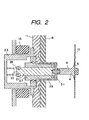
- Fig. 2 shows an enlarged view of the essential portions of a sputtering apparatus which is a second embodiment of the present invention in a cross-sectional view thereof similar to Fig. 1.
- Constituents identical in action with the constituents shown in Fig. 1 are designated by the same reference numerals.
- the distance from the supported position of the slide shaft 21 to the position at which the mask portion 5 abuts against the substrate 10 is great and therefore, when the substrate 10 is rotated, shaft vibration may occur to the slide shaft 21 or the inner mask 4.
- friction may occur in the portion of contact between the spring 25 and the end surface of the slide shaft 21 to thereby cause a load which hampers the inner mask 4 from following the rotation of the substrate 10 to rotate.
- the second embodiment copes with these problems.
- the rotary ball spline 27 is extended to the front surface of the target 18 and also, a thrust bearing 33 is disposed between the end portion of the slide shaft 21 and the end portion of the spring 25.
- a containing chamber 29 protruding toward the substrate and capable of containing the rotary ball spline 27 is formed in the central portion of the backing plate 11.
- This containing portion 29 comprises a cylinder portion inserted in the through-hole 12 formed in the target 18 from the back surface toward the front surface thereof, and a lid portion disposed at the end portion of this cylinder portion which is toward the substrate and having a central aperture.
- the inner diameter of this central aperture is set slightly larger than the outer diameter of the slide shaft 21.
- the slide shaft 21 slightly protrudes from the lid portion of the containing chamber toward the substrate side and has a length which always keeps the protruding state even if the slide shaft slides in the axial direction thereof by the spring 25, and is formed with an internally threaded portion on the end portion thereof toward the substrate.
- One of external threads on an insulating connecting plate 31 formed with externally threaded portions on the opposite surfaces thereof is threadably engaged with the internally threaded portion.
- the other external thread of the insulating connecting plate 31 is threadably engaged with an internally threaded portion formed on the shaft portion 6 of the inner mask 4, whereby the slide shaft 21, the insulating connecting plate 31 and the inner mask 4 are axially made integral with one another.
- the outer wall of the containing chamber 29 can be prevented from being sputtered. Also, by the above-described construction, it becomes possible to support a portion near the center or that end portion of the slide shaft 21 which is toward the substrate by the rotary ball bearing 27, and it becomes possible to prevent shaft vibration from occurring to the slide shaft 21 and the inner mask 4 during the rotation of the substrate. Also, by the thrust bearing 33 being disposed between the rear end portion of the slide shaft 21 and the spring 25, the friction occurring between the end portion of the spring 25 and the slide shaft 21 is reduced and the rotation of the slide shaft 21, etc. about the axis thereof becomes smooth.
- connection between the slide shaft 21 and the inner mask 4 is effected by the insulating connecting plate 31 formed of an insulating material
- the present invention is not restricted thereto.
- the connecting plate 31 may be made of a metal and may be endowed with a role as a so-called earth shield.
- the containing chamber 29 and the shaft portion 6 of the inner mask 4 are of a simple cylindrical shape, they may be of such a shape as partly constitutes, for example, a cone which becomes smaller in its diameter toward the substrate 10.
- the present invention is not restricted thereto, but they may be disposed so as to be horizontally opposed to each other.
- description has been made of a so-called magnetron sputtering apparatus in which a magnetic field by a permanent magnet is added the present invention is not restricted thereto, but the present invention may be applied to a sputtering apparatus using no magnetic field, and may also be applied to a magnetron sputtering apparatus using an electromagnet or the like.
- the application of the present invention is not restricted thereto, but the present invention can be applied to various thin film forming apparatuses such as an evaporation-depositing apparatus and a CVD apparatus.
- the present invention is not only used simply as a method of manufacturing an optical disk or the like, but also is applicable to a process of manufacturing products of which the step of removing the central portions is carried out later, for example, all of disk-shaped members such as hard disks.
- the inner mask By carrying out the present invention, it becomes possible for the inner mask to contact with the surface of the substrate always with a constant and slight load, irrespective of the kind of the substrate or the numbers of the laminated layers of the thin film. Also, film forming in a state in which the substrate and the inner mask are rotated as a unit becomes possible, and it becomes possible to achieve an improvement in the distribution of the film pressure, film nature, etc. of the thin film formed on the substrate.
Landscapes
- Chemical & Material Sciences (AREA)
- Engineering & Computer Science (AREA)
- Chemical Kinetics & Catalysis (AREA)
- Materials Engineering (AREA)
- Mechanical Engineering (AREA)
- Metallurgy (AREA)
- Organic Chemistry (AREA)
- Manufacturing & Machinery (AREA)
- Manufacturing Optical Record Carriers (AREA)
- Physical Vapour Deposition (AREA)
Abstract
In a sputtering apparatus, an inner mask covering the central portion of a substrate is supported by a bearing provided on a backing plate on the back surface of a target, and further this inner mask abuts against the substrate with a predetermined load by a spring. By this construction, when the depositing of thin film is effected, it becomes possible for the inner mask abutting against the substrate to be rotated together with the substrate, and the non-film formed area of the central portion of the substrate is reliably formed and also, an improvement in film thickness, etc. in a film formed area is achieved. <IMAGE>
Description
This invention relates to a thin film forming
apparatus for and a thin film forming method of
forming thin film on a disk-shaped of forming thin
film on a disk-shaped substrate. More particularly,
this invention also relates to a sputtering apparatus
for forming this film by a sputtering method and a
so-called inner mask for use in such apparatus, and a
disk-shaped recording medium manufacturing method of
manufacturing a disk-shaped recording medium such as
an optical disk by the use of such apparatus.
As recording media manufactured with various
kinds of thin film formed on disk-shaped substrates,
and particularly recording media having a disk-kike
shape, there are various disks including, for example,
CD type disks such as CD, CD-R and CD-RW, or optical
disks like DVD type disks such as DVD-ROM and DVD-R,
or magneto-optical disks such as MO and MD.
These disks are manufactured by laminating thin
film on a substrate comprising, for example, a
material such as polycarbonate by the use of one of
various methods such as a sputtering method and a
spin coat method. Generally, the substrate is formed
with a through-hole centrally thereof for use for the
handling of the substrate when the disk is actually
carried on a drive.
Of the laminated thin film, for example, metal
thin film used as reflecting film is formed by the
use of the sputtering method. In this method, a
disk-shaped substrate is fixed and held in opposed
relationship with the front of a target in a vacuum
chamber brought into predetermined pressure by a gas
for discharge such as argon. Generally, in this
state, a certain voltage is given to the target,
whereby discharge occurs between the target and the
substrate, and plasma occurs. A target-constituting
element in the surface of the target is sputtered by
ions in the plasma, and these sputtered particles
adhere to the surface of the substrate, whereby film
forming is effected.
In an optical disk or the like, it is necessary
that a non-film area in which film forming is not
done be provided around a central hole portion
provided in a substrate and on the outer peripheral
portion of the substrate. Therefore, during the film
forming by sputtering, the actual film forming
process is carried out with the non-film formed area
covered with jigs called an inner mask and an outer
mask. This non-film formed area has its width
determined by a standard, and a predetermined value
must be obtained irrespective of the substrate.
Therefore, in a conventional sputtering
apparatus, it has been the practice to fix both of
the outer mask and the inner mask to the apparatus,
and cover the inner and outer peripheries of the
substrate with the substrate brought into contact
with or proximity to these masks having had their
positional relation defined. Regarding the inner
mask, however, a construction such as a beam for
fixing this mask to the apparatus has been required,
and the presence of this construction between the
target and the substrate has led to the possibility
that the uniformity of the thin film formed may be
deteriorated.
As a countermeasure for that, there has been
proposed such a sputtering apparatus as disclosed,
for example, in Japanese Patent Application Laid-Open
No. H7-331434. In this apparatus, an inner mask
extends from the central portion of a target
positionally corresponding to the center of a
substrate toward the central portion of the substrate.
That is, a fulcrum for supporting the inner mask is
provided so as to extend perpendicularly to the
surface of the target and from this surface to the
substrate, thereby suppressing the influence of the
fulcrum during thin film forming.
As previously described, the width of the non-film
formed area is required to assume a
predetermined value without becoming uneven for each
substrate. At the same time, the profile such as the
film thickness of the thin film in a film formed area
is required to exhibit a uniform value up to as near
as possible to the boundary portion between the non-film
formed area and the film formed area.
Accordingly, it is preferable that the inner
peripheral end portion of the outer mask and the
outer peripheral end portion of the inner mask be in
close contact with the substrate to thereby minimize
the influence upon the other portions than the non-film
formed area.
The substrate is generally formed of an elastic
material such as polycarbonate and therefore, may not
be plastically deformed even if it is urged against
the outer mask or the inner mask by a conveying
apparatus or the like with a certain degree of load.
However, when some layers of thin film are already
formed on the substrate, the contact of the outer
mask and the inner mask with those layers of thin
film may give an injury such as breakage to those
layers of thin film. Such a sputtering apparatus as
disclosed in Japanese Patent Application Laid-Open No.
H7-331434 wherein the inner mask is firmly fixed is
considered to be high in the possibility that such an
injury as mentioned above may occur.
Further, in this apparatus, when the substrate
used is changed, it is required to change the fixed
position of the inner mask in conformity with the
substrate at any time, but this adjustment is
considered to be not easy. Accordingly, it is
considered to be difficult to adapt this apparatus to
various substrates. Also, when the recording density
of an optical disk or the like becomes higher and the
wavelength of a laser beam used for reading or the
like becomes shorter, it is desired to more improve
the distribution of a film thickness or the like in
the thin film obtained at present.
The present invention has been made in view of
the above-noted task, and an object thereof is to
provide a thin film forming apparatus which enables
an inner mask to always contact with the surface of a
substrate with a constant and slight load,
irrespective of the kind of the substrate or the
number of the laminated layers of formed thin film.
Also, an object of the present invention is to
provide a thin film forming apparatus which can
improve the distribution of the film pressure, film
nature, etc. of thin film formed on a substrate.
In order to solve the above-noted task, a
sputtering apparatus according to the present
invention is a sputtering apparatus for effecting
film forming on the surface of a substrate having a
substantially disk-like shape in a vacuum chamber,
the sputtering apparatus having a target comprising a
main constituent element of film to be formed, a
backing plate for holding the target by the surface
thereof, a substrate holder for holding the substrate
and rightly opposing the surface of the substrate to
the target, and an outer mask and an inner mask
covering the outer peripheral position and central
portion, respectively, of the substrate, wherein the
inner mask communicates with and is supported by a
slide shaft extending through a through-hole formed
in the target and supported by a bearing disposed on
the backing plate for masking rotation and
translation possible, and abuts against the central
portion of the substrate through the slide shaft with
a predetermined load by biasing means disposed on the
backing plate.
In the above-described sputtering apparatus, it
is preferable that the biasing means comprise a
spring disposed at an end portion differing from an
end portion of the slide shaft which communicates
with the inner mask. Also, it is preferable that the
slide shaft have a portion formed of an insulating
material in the portion thereof communicating with
the inner mask. Also, it is preferable that the
biasing means bias the slide shaft through a thrust
bearing.
Further, in the above-described sputtering
apparatus, it is preferable that the backing plate
protrude from the surface of the target and have a
containing chamber formed with an aperture having an
inner diameter slightly larger than the diameter of
the slide shaft at a location rightly opposed to the
center of the substrate, and the slide shaft
protruding from the aperture toward the substrate,
the bearing and the biasing means be contained in the
containing chamber.
Also, in order to solve the above-noted task, a
thin film forming method according to the present
invention is a method of forming thin film on a
substrate having a substantially disk-like shape, the
method comprising disposing a target formed of a main
constituent material of the thin film, fixing the
substrate onto a holder rightly opposed to the target
and rotatable about a predetermined axis, causing an
inner mask connected to a shaft member extending from
the back surface of the target to the front surface
of the target through a through-hole formed in the
target with the predetermined axis as the center to
abut against a predetermined area of the central
portion of the substrate, causing plasma to occur
between the substrate and the target, sputtering the
front surface of the target by ions in the plasma,
and depositing on the surface of the substrate thin
film having the component of the target as a main
constituent element, wherein the inner mask abuts
against the substrate with a predetermined load, and
when the depositing of the thin film is effected, the
inner mask is rotated about the predetermined axis
together with the substrate.
Also, a disk-shaped recording medium
manufacturing method according to the present
invention is a disk-shaped recording medium
manufacturing method of forming particular film on a
disk-shaped recording medium, the method comprising
disposing a target formed of a main constituent
material of the particular film, fixing a
substantially disk-shaped substrate onto a holder
rightly opposed to the target and rotatable about a
predetermined axis, causing an inner mask connected
to a shaft member extending from the back surface of
the target to the front surface of the target through
a through-hole formed in the target with the
predetermined axis as the center to abut against a
predetermined area of the central portion of the
substrate, causing plasma to occur between the
substrate and target, sputtering the front surface of
the target by ions in the plasma, and depositing the
particular film on the surface of the substrate,
wherein the inner mask abuts against the substrate
with a predetermined load, and when the depositing of
the thin film is effected, the inner mask is rotated
about the predetermined axis together with the
substrate.
Fig. 1 schematically shows the construction of
a cross section of a sputtering apparatus which is a
first embodiment of the present invention when a
substrate is disposed at a thin film forming position
in the apparatus and the apparatus is in a state for
effecting film forming. In the present embodiment,
description will be made of a magnetron sputtering
apparatus in which electron catching probability is
enhanced by the effect of a magnetic field formed by
a permanent magnet or the like to thereby enhance the
rate of sputtering.
In the sputtering apparatus, there are usually
disposed various constructions such as a construction
called an earth shield used to restrict a discharge
space to a particular area near a target, a
construction called an adherence preventing shield
for preventing the adherence of unnecessary sputter
particles to the interior of the apparatus, and a
construction used for the conveyance of a substrate.
These constructions, however, have no direct relation
with the present invention and therefore need not be
shown and described herein. Of course, however,
these becomes necessary as the actual construction of
the apparatus.
As shown in Fig. 1, the sputtering apparatus
according to the present invention has a cathode
electrode 9 constituted by a backing plate 11 to
which cooling water is introduced by a cooling water
circulating mechanism, not shown, a permanent magnet
15 disposed on the back surface of the backing plate
11, and a target 18 fixed to the front surface of the
backing plate 11. In front of this target 18, there
are disposed an outer mask 7 and a substrate 10
supported by a substrate holder 3 rotatable about an
axis. The mask 7 is fixed to and supported on the
substrate holder 3 by a magnet, not shown.
At the centers of the backing plate 11 and the
target 18, there is formed a through-hole 12
extending from the back surfaces to the front
surfaces thereof, and a slide shaft 21 formed of an
insulating material such as ceramics is inserted in
the through-hole 12. The rear end portion of the
slide shaft 21 is contained in a spring containing
chamber 23 provided in the back surface of the
backing plate 11, and is biased toward the fore end
of the shaft by a spring 25 which is biasing means
contained in the spring containing chamber 23.
The spring containing chamber 23 has a bottomed
cylindrical shape having a flange portion 24 jutting
out at an opening end, and is fixed to the back
surface of the backing plate 11 at the flange portion
24. The vicinity of the rear end portion of the
slide shaft 21 is supported for rotation about the
axis thereof and translation in the direction of the
axis thereof by a rotary ball spline 27 disposed in
the spring containing chamber 23.
The surrounding wall constituting the spring
containing chamber 23, the spring 25 and the rotary
ball sprine 27 are designed to assume the same
potential as the backing plate 11. An inner mask 4
should preferably assume the same potential as the
substrate 10, or earth potential and therefore, the
slide shaft 21 is partly formed of an insulating
material to thereby achieve the electrical insulation
between the inner mask 4 and the rotary ball spline
27 or the like.
The inner mask 4 is comprised of a mask portion
5 for actually covering the inner peripheral portion
of the substrate as the inner mask, and a shaft
portion 6 communicating with this mask portion. The
shaft portion 6 is internally threaded on an end
portion thereof differing from an end portion
connected to the mask portion 5, and is threadably
engaged with external thread formed on the distal end
of the slide shaft 21, whereby it is made integral
with the slide shaft 21 coaxially therewith. The
mask portion 5 abuts against the central portion of
the substrate 10, and covers a predetermined range of
non-film formed area on the central portion of the
substrate 10.
The mask portion 5 is biased toward the surface
of the substrate by the spring 25. By making the
biasing force of this spring 25 suitable, it becomes
possible for the inner mask 4 to abut against the
surface of the substrate 10 always with a constant
and slight load. Also, by the inner mask 4 being
rotatably supported through the slide shaft 21, the
inner mask 4 becomes rotatable about the axis of the
inner mask 4 together with the substrate 10. By this
construction, it becomes possible to rotate the
substrate about the axis actually during film forming
and therefore, the distribution of the film thickness,
etc. in the formed thin film is greatly improved.
Description will now be made of the procedure
of actually effecting thin film forming on the
substrate by the use of the sputtering apparatus
according to the present embodiment. First, the
substrate holder 3 receives the substrate 10 from a
conveying apparatus with the outer mask 7 at a
substrate receiving position. The holder 3
supporting the substrate 10 is driven to a position
rightly opposed to the cathode electrode 9 by a
holder driving mechanism, and approaches the cathode
electrode 9 so that the interval between the surface
of the substrate 10 and the surface of the cathode
electrode 9 may assume a predetermined value. At
this time, the mask portion 5 of the inner mask 4
abuts against a position corresponding to a non-film
formed area on the inner peripheral side of the
substrate. Also, a supporting member, not shown, for
the cathode electrode and the holder driving
mechanism are united to thereby form a vacuum vessel.
Subsequently, exhaust from the interior of the
vacuum vessel is done by an exhaust system, not shown,
and the pressure in the vacuum vessel is reduced to
predetermined pressure, whereafter a gas for
discharge such as argon is introduced into the vacuum
vessel, and the pressure in the vacuum vessel is
increased to discharge starting pressure by this gas.
At the same time, rotation about the center of the
substrate 10 held by the holder 3 is started. In
this state, a predetermined voltage is applied to the
cathode electrode 9, and the occurrence of discharge
and the production of plasma are done between the
target 18 and the substrate 10. The surface of the
target is sputtered by ions produced in this plasma,
and the sputtered particles adhere to and deposit on
the substrate, whereby the forming of thin film is
done.
The plasma is maintained for a predetermined
time to thereby form thin film of a desired thickness,
whereafter the application of the voltage to the
cathode electrode 9 is stopped to thereby make the
plasma disappear, thus terminating the forming of the
thin film. Subsequently, a gas for purge such as dry
nitrogen is introduced into the vacuum vessel to
thereby make the pressure in the vacuum vessel equal
to or higher than the atmospheric pressure, and the
supporting member for the cathode electrode 9 and the
holder driving mechanism are separated from each
other. Subsequently, the substrate on which the film
has been formed and the masks are removed from the
retracted holder, and the film forming process is
completed.
As described above, by the adoption of the
construction according to the present invention, it
becomes possible for the inner mask 4 to abut against
the substrate 10 with a slight and constant load, and
even if the substrate is rotated during film forming,
the inner mask 4 and the substrate 10 do not mutually
slide and therefore, it becomes possible to obtain
good distribution of film thickness, etc. without
injuring the substrate.
In the present embodiment, use is made of a
substrate not formed with a through-hole centrally
thereof and provided with a projection on the back
side of the film formed surface thereof. The present
invention, however, is not restricted thereto, but
use may be made of a substrate having a through-hole
in the central portion thereof. In that case, in
order that during thin film forming, the inner mask 4
and the substrate holder 3 may assume the same
potential, a spring or the like may be disposed on
that surface of the central portion of the inner mask
4 which is adjacent to the surface of the substrate
or that surface of the substrate holder 3 which is
rightly opposed to the inner mask 4, and this spring
may be used as the contact between the inner mask 4
and the substrate holder 3.
Also, while the slide shaft 21 is constructed
as a single piece formed of an insulating material,
the present invention is not restricted thereto, but
the slide shaft 21 may be comprised of such a
plurality of members as comprise an electrical
conductor and an insulator connected together. Also,
the method of connecting the slide shaft 21 and the
inner mask 4 is not restricted to the threadable
engagement by the mutual threaded structure, but it
is possible to use one of various coupling methods.
Also, as the backing plate 11, use is generally made
of one formed of copper which is easy to work and is
high in heat conductivity and can be easily water-cooled
as a whole, but it is desirable that the wall
of the spring containing chamber 23 be also formed of
copper so that the rotary ball spline 27 can be
cooled at the same time.
Fig. 2 shows an enlarged view of the essential
portions of a sputtering apparatus which is a second
embodiment of the present invention in a cross-sectional
view thereof similar to Fig. 1.
Constituents identical in action with the
constituents shown in Fig. 1 are designated by the
same reference numerals. In the construction of Fig.
1, the distance from the supported position of the
slide shaft 21 to the position at which the mask
portion 5 abuts against the substrate 10 is great and
therefore, when the substrate 10 is rotated, shaft
vibration may occur to the slide shaft 21 or the
inner mask 4. Also, friction may occur in the
portion of contact between the spring 25 and the end
surface of the slide shaft 21 to thereby cause a load
which hampers the inner mask 4 from following the
rotation of the substrate 10 to rotate. The second
embodiment copes with these problems.
Specifically, the rotary ball spline 27 is
extended to the front surface of the target 18 and
also, a thrust bearing 33 is disposed between the end
portion of the slide shaft 21 and the end portion of
the spring 25. In order to extend the rotary ball
spline 27 toward the substrate, a containing chamber
29 protruding toward the substrate and capable of
containing the rotary ball spline 27 is formed in the
central portion of the backing plate 11. This
containing portion 29 comprises a cylinder portion
inserted in the through-hole 12 formed in the target
18 from the back surface toward the front surface
thereof, and a lid portion disposed at the end
portion of this cylinder portion which is toward the
substrate and having a central aperture. The inner
diameter of this central aperture is set slightly
larger than the outer diameter of the slide shaft 21.
The slide shaft 21 slightly protrudes from the
lid portion of the containing chamber toward the
substrate side and has a length which always keeps
the protruding state even if the slide shaft slides
in the axial direction thereof by the spring 25, and
is formed with an internally threaded portion on the
end portion thereof toward the substrate. One of
external threads on an insulating connecting plate 31
formed with externally threaded portions on the
opposite surfaces thereof is threadably engaged with
the internally threaded portion. The other external
thread of the insulating connecting plate 31 is
threadably engaged with an internally threaded
portion formed on the shaft portion 6 of the inner
mask 4, whereby the slide shaft 21, the insulating
connecting plate 31 and the inner mask 4 are axially
made integral with one another.
By this insulating connecting plate 31 being
disposed, the outer wall of the containing chamber 29
can be prevented from being sputtered. Also, by the
above-described construction, it becomes possible to
support a portion near the center or that end portion
of the slide shaft 21 which is toward the substrate
by the rotary ball bearing 27, and it becomes
possible to prevent shaft vibration from occurring to
the slide shaft 21 and the inner mask 4 during the
rotation of the substrate. Also, by the thrust
bearing 33 being disposed between the rear end
portion of the slide shaft 21 and the spring 25, the
friction occurring between the end portion of the
spring 25 and the slide shaft 21 is reduced and the
rotation of the slide shaft 21, etc. about the axis
thereof becomes smooth.
While in the present embodiment, the connection
between the slide shaft 21 and the inner mask 4 is
effected by the insulating connecting plate 31 formed
of an insulating material, the present invention is
not restricted thereto. Generally, when the inner
mask 4 is to be brought to the same potential as the
substrate holder 10 or earth potential by the
utilization of an aperture portion provided centrally
of the substrate, the connecting plate 31 may be made
of a metal and may be endowed with a role as a so-called
earth shield. Also, while the containing
chamber 29 and the shaft portion 6 of the inner mask
4 are of a simple cylindrical shape, they may be of
such a shape as partly constitutes, for example, a
cone which becomes smaller in its diameter toward the
substrate 10.
Also, while a construction in which the cathode
electrode and the substrate are upright and rightly
opposed to each other has been shown as the
embodiment, the present invention is not restricted
thereto, but they may be disposed so as to be
horizontally opposed to each other. Also, while in
the present embodiment, description has been made of
a so-called magnetron sputtering apparatus in which a
magnetic field by a permanent magnet is added, the
present invention is not restricted thereto, but the
present invention may be applied to a sputtering
apparatus using no magnetic field, and may also be
applied to a magnetron sputtering apparatus using an
electromagnet or the like.
Also, while a sputtering apparatus has been
mentioned as a thin film forming apparatus which
becomes a subject when the present invention is used,
the application of the present invention is not
restricted thereto, but the present invention can be
applied to various thin film forming apparatuses such
as an evaporation-depositing apparatus and a CVD
apparatus. Also, the present invention is not only
used simply as a method of manufacturing an optical
disk or the like, but also is applicable to a process
of manufacturing products of which the step of
removing the central portions is carried out later,
for example, all of disk-shaped members such as hard
disks.
By carrying out the present invention, it
becomes possible for the inner mask to contact with
the surface of the substrate always with a constant
and slight load, irrespective of the kind of the
substrate or the numbers of the laminated layers of
the thin film. Also, film forming in a state in
which the substrate and the inner mask are rotated as
a unit becomes possible, and it becomes possible to
achieve an improvement in the distribution of the
film pressure, film nature, etc. of the thin film
formed on the substrate.
Claims (7)
- A sputtering apparatus for effecting film forming on a surface of a substrate having a substantially disk-like shape in a vacuum chamber, having:wherein said inner mask communicates with and is supported by a slide shaft extending through a through-hole formed in said target and supported by a bearing disposed on said backing plate for making rotation and translation possible, and abuts against the central portion of said substrate through said slide shaft with a predetermined load by biasing means disposed on said backing plate.a target comprising a main constituent element of film to be formed;a backing plate for holding said target by a surface of said target;a substrate holder for holding said substrate and rightly opposing the surface of said substrate to said target; andan outer mask and an inner mask covering an outer peripheral portion and a central portion, respectively, of said substrate;
- A sputtering apparatus according to Claim 1, wherein said biasing means comprises a spring disposed at an end portion differing from an end portion of said slide shaft which communicates with said inner mask.
- A sputtering apparatus according to Claim 1, wherein said slide shaft has a portion formed of an insulating material in a portion thereof communicating with said inner mask.
- A sputtering apparatus according to Claim 1, wherein said biasing means biases said slide shaft through a thrust bearing.
- A sputtering apparatus according to Claim 1, wherein said backing plate protrude from a surface of said target and has a containing chamber formed with an aperture having an inner diameter slightly larger than a diameter of said slide shaft at a location rightly opposed to the center of said substrate, and the slide shaft protruding from said aperture toward said substrate, said bearing and said biasing means are contained in said containing chamber.
- A thin film forming method of forming thin film on a substrate having a substantially disk-like shape, comprising:wherein said inner mask abuts against said substrate with a predetermined load, and when the depositing of said thin film is effected, said inner mask is rotated about said predetermined axis together with said substrate.disposing a target formed of a main constituent material of said thin film;fixing said substrate onto a holder rightly opposed to said target and rotatable about a predetermined axis;causing an inner mask connected to a shaft member extending from a back surface of said target to a front surface of said target through a through-hole formed in said target with said predetermined axis as the center to abut against a predetermined area of a central portion of said substrate;causing plasma to occur between said substrate and said target;sputtering the front surface of said target by ions in said plasma; anddepositing on a surface of said substrate thin film having a component of said target as a main constituent element;
- A disk-shaped recording medium manufacturing method of forming particular film on a disk-shaped recording medium, comprising:wherein said inner mask abuts against said substrate with a predetermined load, and when the depositing of said particular film is effected, said inner mask is rotated about said predetermined axis together with said substrate.disposing a target formed of a main constituent material of said particular film;fixing a substantially disk-shaped substrate onto a holder rightly opposed to said target and rotatable about a predetermined axis;causing an inner mask connected to a shaft member extending from a back surface of said target to a front surface of said target through a through-hole formed in said target with said predetermined axis as the center to abut against a predetermined area of a central portion of said substrate;causing plasma to occur between said substrate and said target;sputtering the front surface of said target by ions in said plasma; anddepositing said particular film on a surface of said substrate;
Applications Claiming Priority (3)
| Application Number | Priority Date | Filing Date | Title |
|---|---|---|---|
| JP2002102038A JP2003293131A (en) | 2002-04-04 | 2002-04-04 | Sputtering system, method for forming thin film by sputtering, and method for manufacturing disk-shaped recording medium using the sputtering system |
| JP2002102038 | 2002-04-04 | ||
| PCT/JP2003/004170 WO2003085158A1 (en) | 2002-04-04 | 2003-04-01 | Spattering device, method of forming thin film by spattering, and method of manufacturing disk-like recording medium using the device |
Publications (2)
| Publication Number | Publication Date |
|---|---|
| EP1496135A1 true EP1496135A1 (en) | 2005-01-12 |
| EP1496135A4 EP1496135A4 (en) | 2008-05-21 |
Family
ID=28786246
Family Applications (1)
| Application Number | Title | Priority Date | Filing Date |
|---|---|---|---|
| EP03715704A Withdrawn EP1496135A4 (en) | 2002-04-04 | 2003-04-01 | Spattering device, method of forming thin film by spattering, and method of manufacturing disk-like recording medium using the device |
Country Status (6)
| Country | Link |
|---|---|
| EP (1) | EP1496135A4 (en) |
| JP (1) | JP2003293131A (en) |
| KR (1) | KR20040094909A (en) |
| CN (1) | CN1646723A (en) |
| TW (1) | TWI229144B (en) |
| WO (1) | WO2003085158A1 (en) |
Cited By (1)
| Publication number | Priority date | Publication date | Assignee | Title |
|---|---|---|---|---|
| CN101692485B (en) * | 2009-09-30 | 2011-11-02 | 东莞宏威数码机械有限公司 | sealing box |
Families Citing this family (3)
| Publication number | Priority date | Publication date | Assignee | Title |
|---|---|---|---|---|
| CN100431023C (en) * | 2004-09-23 | 2008-11-05 | 精碟科技股份有限公司 | Apparatus for manufacturing optical information storage medium |
| TWI396766B (en) * | 2005-03-11 | 2013-05-21 | 索雷拉斯先進塗料公司 | Flat end block for supporting a rotatable sputtering target |
| RU2653897C2 (en) * | 2016-10-18 | 2018-05-15 | Публичное акционерное общество "Сатурн" (ПАО "Сатурн") | Device for spraying an antireflection coating of a photoconverter |
Family Cites Families (6)
| Publication number | Priority date | Publication date | Assignee | Title |
|---|---|---|---|---|
| JPH07331434A (en) * | 1994-06-07 | 1995-12-19 | Sony Disc Technol:Kk | Magnetron sputtering system |
| JP3096258B2 (en) * | 1997-07-18 | 2000-10-10 | 芝浦メカトロニクス株式会社 | Each leaf type magnetron sputtering system |
| JP4037493B2 (en) * | 1997-10-28 | 2008-01-23 | 芝浦メカトロニクス株式会社 | Film forming apparatus provided with substrate cooling means |
| JP2000315337A (en) * | 1999-04-30 | 2000-11-14 | Fuji Photo Film Co Ltd | Manufacture of recording medium |
| JP2000315339A (en) * | 1999-04-30 | 2000-11-14 | Fuji Photo Film Co Ltd | Manufacture of recording medium |
| JP2001176137A (en) * | 1999-12-14 | 2001-06-29 | Fuji Photo Film Co Ltd | Method for manufacturing recording medium |
-
2002
- 2002-04-04 JP JP2002102038A patent/JP2003293131A/en active Pending
-
2003
- 2003-04-01 KR KR10-2004-7015733A patent/KR20040094909A/en not_active Ceased
- 2003-04-01 EP EP03715704A patent/EP1496135A4/en not_active Withdrawn
- 2003-04-01 WO PCT/JP2003/004170 patent/WO2003085158A1/en not_active Ceased
- 2003-04-01 CN CNA038077183A patent/CN1646723A/en active Pending
- 2003-04-03 TW TW092107658A patent/TWI229144B/en not_active IP Right Cessation
Cited By (1)
| Publication number | Priority date | Publication date | Assignee | Title |
|---|---|---|---|---|
| CN101692485B (en) * | 2009-09-30 | 2011-11-02 | 东莞宏威数码机械有限公司 | sealing box |
Also Published As
| Publication number | Publication date |
|---|---|
| EP1496135A4 (en) | 2008-05-21 |
| CN1646723A (en) | 2005-07-27 |
| TW200306357A (en) | 2003-11-16 |
| TWI229144B (en) | 2005-03-11 |
| KR20040094909A (en) | 2004-11-10 |
| WO2003085158A1 (en) | 2003-10-16 |
| JP2003293131A (en) | 2003-10-15 |
Similar Documents
| Publication | Publication Date | Title |
|---|---|---|
| US6455101B1 (en) | Method for depositing a protective carbon coating on a data recording disk | |
| US20080251376A1 (en) | Vacuum Processing Device and Method of Manufacturing Optical Disk | |
| JP2962912B2 (en) | Sputter cathode for coating substrates with cathode sputtering equipment | |
| KR100532805B1 (en) | Apparatus and method for depositing a film on a substrate | |
| JPH01255666A (en) | Sputter source having rapid replaceable target and adaptor ring | |
| JPS5844742B2 (en) | sputtering equipment | |
| US5328583A (en) | Sputtering apparatus and process for forming lamination film employing the apparatus | |
| US6022462A (en) | DC sputtering system | |
| JP3957173B2 (en) | Substrate delivery method to disk-shaped substrate deposition apparatus, substrate delivery mechanism and substrate holder used in the method, and disc-shaped recording medium manufacturing method using the method | |
| US6083364A (en) | Magnetron sputtering apparatus for single substrate processing | |
| US6066242A (en) | Conical sputtering target | |
| JP3398452B2 (en) | Sputtering equipment | |
| JP2003293131A (en) | Sputtering system, method for forming thin film by sputtering, and method for manufacturing disk-shaped recording medium using the sputtering system | |
| US8591706B2 (en) | Sputtering system and method for depositing thin film | |
| KR100594527B1 (en) | Substrate guiding method, substrate guiding mechanism and mask used in the above method for film forming apparatus for disc-shaped substrate, and manufacturing method of disk-type recording medium using the above method | |
| JP2004022153A (en) | Method for transferring substrate to disk substrate film forming device, substrate transferring mechanism and substrate holder used in the method, and manufacturing method of disk recording medium using the method | |
| KR100602528B1 (en) | Disc type substrate chucking apparatus and method, and method for manufacturing disc type recording medium using the apparatus | |
| JPH07331434A (en) | Magnetron sputtering system | |
| JP2005018814A (en) | Inner mask for disk-shaped substrate, inner mask and outer mask for film forming device, receiving and delivering method of substrate, and manufacturing method of disk-shaped recording medium using method | |
| JP2001240962A (en) | Sputtering apparatus for optical disk | |
| JPH10102248A (en) | Spatter equipment | |
| JPH05320900A (en) | Substrate holder and substrate holding method | |
| KR20050021018A (en) | Method for delivery of substrate to film forming device for disk-like substrate, substrate delivery mechanism and substrate holder used for the method, and method of manufacturing disk-like recording medium using the method |
Legal Events
| Date | Code | Title | Description |
|---|---|---|---|
| PUAI | Public reference made under article 153(3) epc to a published international application that has entered the european phase |
Free format text: ORIGINAL CODE: 0009012 |
|
| 17P | Request for examination filed |
Effective date: 20041027 |
|
| AK | Designated contracting states |
Kind code of ref document: A1 Designated state(s): CH DE LI |
|
| AX | Request for extension of the european patent |
Extension state: AL LT LV MK |
|
| A4 | Supplementary search report drawn up and despatched |
Effective date: 20080418 |
|
| STAA | Information on the status of an ep patent application or granted ep patent |
Free format text: STATUS: THE APPLICATION IS DEEMED TO BE WITHDRAWN |
|
| 18D | Application deemed to be withdrawn |
Effective date: 20050613 |