EP1494363A2 - Method for cancelling noise in a mobile terminal - Google Patents
Method for cancelling noise in a mobile terminal Download PDFInfo
- Publication number
- EP1494363A2 EP1494363A2 EP04015392A EP04015392A EP1494363A2 EP 1494363 A2 EP1494363 A2 EP 1494363A2 EP 04015392 A EP04015392 A EP 04015392A EP 04015392 A EP04015392 A EP 04015392A EP 1494363 A2 EP1494363 A2 EP 1494363A2
- Authority
- EP
- European Patent Office
- Prior art keywords
- noise
- idle slot
- terminal
- slot
- tdma
- Prior art date
- Legal status (The legal status is an assumption and is not a legal conclusion. Google has not performed a legal analysis and makes no representation as to the accuracy of the status listed.)
- Withdrawn
Links
- 238000000034 method Methods 0.000 title claims abstract description 43
- 230000005540 biological transmission Effects 0.000 claims description 7
- 238000001228 spectrum Methods 0.000 description 4
- 238000010295 mobile communication Methods 0.000 description 3
- 238000004891 communication Methods 0.000 description 2
- 238000010586 diagram Methods 0.000 description 2
- 230000001629 suppression Effects 0.000 description 2
- HBBGRARXTFLTSG-UHFFFAOYSA-N Lithium ion Chemical compound [Li+] HBBGRARXTFLTSG-UHFFFAOYSA-N 0.000 description 1
- 238000004590 computer program Methods 0.000 description 1
- 230000006870 function Effects 0.000 description 1
- 229910001416 lithium ion Inorganic materials 0.000 description 1
- 238000012986 modification Methods 0.000 description 1
- 230000004048 modification Effects 0.000 description 1
- 230000001360 synchronised effect Effects 0.000 description 1
Images


Classifications
-
- H—ELECTRICITY
- H04—ELECTRIC COMMUNICATION TECHNIQUE
- H04B—TRANSMISSION
- H04B15/00—Suppression or limitation of noise or interference
-
- H—ELECTRICITY
- H04—ELECTRIC COMMUNICATION TECHNIQUE
- H04B—TRANSMISSION
- H04B15/00—Suppression or limitation of noise or interference
- H04B15/02—Reducing interference from electric apparatus by means located at or near the interfering apparatus
-
- H—ELECTRICITY
- H04—ELECTRIC COMMUNICATION TECHNIQUE
- H04B—TRANSMISSION
- H04B2215/00—Reducing interference at the transmission system level
- H04B2215/061—Reduction of burst noise, e.g. in TDMA systems
-
- H—ELECTRICITY
- H04—ELECTRIC COMMUNICATION TECHNIQUE
- H04B—TRANSMISSION
- H04B2215/00—Reducing interference at the transmission system level
- H04B2215/061—Reduction of burst noise, e.g. in TDMA systems
- H04B2215/063—Reduction of burst noise, e.g. in TDMA systems by smoothing the transmission power envelope
Definitions
- the present invention generally relates to mobile communication systems, and more particularly to a system and method for canceling noise in a mobile terminal.
- CDMA Code Division Multiple Access
- TDMA Time Division Multiple Access
- GSM Global System for Mobile communications
- FDMA Frequency Division Multiple Access
- noise is generated from an audio output terminal due to a time burst ripple on a battery power line. This form of noise is called TDMA noise.
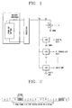
- FIG. 1 shows a power unit of a mobile terminal. This unit is designed so that its audio power terminal is separately formed and one or more audio-exclusive Low Drop Output regulators (LDOs) are used to minimize influence of noise within an audio frequency range caused by ripple in a power terminal of an audio amplifier.
- LDOs Low Drop Output regulators
- the Figure 1 power unit When operated in accordance with a related-art method, the Figure 1 power unit merely focuses on minimizing TDMA noise after it has been created. This method does not prevent the generation of TDMA noise at its source. Also, because additional circuits such as the audio power terminal and audio-purpose power regulator are used, the related-art method does not promote miniaturization, which is the recent trend in mobile terminal design.
- An object of the invention is to solve at least the above problems and/or disadvantages and to provide at least the advantages described hereinafter.
- Another object of the present invention is to provide a system and method for more effectively canceling TDMA noise in a mobile terminal used in a communication system, including but not limited to a GSM system.
- the present invention provides a system and method for canceling noise in a mobile terminal including: a step in which when a time burst is generated on a battery power line, it is checked whether a current time slot is an idle slot; a step in which if the current time slot is the idle slot, a noise level is applied to generate an offset voltage; and a step in which an overall battery voltage drop is reduced.
- the noise level can be supplied by applying an arbitrary channel when the current time slot is the idle slot in a baseband, or can be suitably supplied as a transceiver generates a thermal noise in the idle slot state.
- the present invention is a system and method for canceling noise which is preferably applied to a mobile terminal of a mobile communication system, which includes but is not limited to a GSM system. If desired, the method may also be used for terminals that conform to other communication standards and/or protocols. When applied in this manner, the present invention advantageously reduces audio frequency noise of a power terminal, which, in turn, suppresses or cancels TDMA noise generated at the mobile terminal.
- Figure 2 shows a structure of a TDMA time frame
- Figure 3 is a graph showing a relationship between current amplified by a time burst and a voltage drop in accordance with a related-art terminal.
- a basic TDMA unit is referred to as a time slot (or burst period), which has a predetermined duration of, for example, 15/26 ms (that is, about 577 ⁇ s) for some applications.
- One TDMA frame typically includes 8 time slots (#0 - #7). With this format, eight calls can be simultaneously maintained per channel. Also, one TDMA frame has a length of 577 ⁇ s*8; that is, about 4.615ms. In a GSM system, data is transmitted in only one allocated time slot of one frame of TDMA, while the other seven time slots are in an idle state.
- a power amplifier (PA) of the terminal raises a pulse current up to a maximum value for one time slot period, e.g., 2.5A for a 577 ⁇ s period.
- This rise in pulse current derives from a terminal battery and may be repeatedly performed every TDMA frame period (e.g., 4.615ms) as long as data transmission is performed.
- Figure 4 is a graph showing a frequency spectrum of a power ripple generated by a voltage drop during a GSM burst.
- a frequency distribution is shown where a frequency C1 of 217 Hz is obtained during a time period of one TDMA frame (e.g., 4.615ms).
- the size of C1 is proportional to a degree of the voltage drop in Figure 3.
- C2, C3, C4,..., CN are harmonic components and frequency spectrums in an audible range in which every person can listen.
- a predetermined harmonic e.g., sixth harmonic
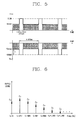
- Figure 5 is a graph showing generation of an offset voltage according to a preferred embodiment of the present invention
- Figure 6 is a graph showing a power ripple reduction achieved according to a battery voltage drop resulting from the offset voltage in Figure 5.
- a terminal battery experiences a voltage drop when current I PA is amplified by the power amplifier during or just prior to data transmission; that is, during an active time slot.
- this voltage drop is reduced by applying an arbitrary noise level to one or more idle slots in the TDMA frame.
- the present invention generates a noise signal during an idle slot to thereby generate an offset voltage (V offset ).
- V offset reduces an overall voltage drop difference by an amount ⁇ , and this causes a proportional reduction of the TDMA noise component, e.g., up to the sixth harmonic.
- the noise signal applied during the idle slot reduces the voltage drop between an active slot and the idle slot, it is not actually transmitted through an antenna. This is because an antenna switch at a rear stage of the power amplifier does not transmit data (e.g., is switched off) during idle time slot periods.
- a suitable value of the noise level to be applied may differ depending on a voltage drop value during the time burst, or depending on power supply rejection ratio (PSRR) characteristics values of the audio amplifier.
- PSRR is a value indicative of performance of removing a spectrum component in the audio frequency. Most components have a value of about -70dB in the frequency of 200Hz - 1.5kHz. Thus, in order to cancel TDMA noise, a PSSR characteristics value of about -80dB may be obtained and therefore about -10dB of ripple level may be additionally reduced calculatively.
- C1 may be about 25mV (28dBm), which is a reduction of less than 10dB. Accordingly, a fundamental noise level generated during the idle slot needs only to correspond to about 50mV (75mV - 25mV). In this respect, however, a greater V offset value of about 70mV - 100mV may be generated in consideration of other harmonic components inclusive. Thus, a noise level to be generated during the idle slot should be about 70mV - 100mV. However, this is only a theoretically calculated value and there can be some difference depending on the voltage drop value as mentioned above.
- the transmitter is operated in a normal manner with the antenna switched on during an active time slot.
- a noise signal may be generated during all, a portion, or just one of the idle time slots in a TDMA frame. This will create the offset voltage required to achieve the desired noise suppression.
- FIG. 7 is a flow chart showing steps included in a method for canceling noise of a mobile terminal in accordance with a preferred embodiment of the present invention.
- a time burst is generated on the battery power line (step S10)
- a check is performed to determine whether a current time slot is an idle slot (step S20).
- the time burst may be detected by a detector in the terminal.
- the detector may be, for example, a processor (e.g., an MSM or other integrated circuit chip) in the terminal. If the current time slot is an idle slot, a noise level is applied (step S30). Then, an offset voltage is generated (step S40) and accordingly an overall battery voltage drop is reduced (step S50). This reduction of the battery voltage drop corresponds to or is effected by a reduction of the TDMA noise component.
- the method for canceling noise of a mobile terminal in accordance with the present invention has at least the following advantages. Since the ripple of overall battery power is reduced by reducing the battery voltage drop due to the power amplifier, power can be stably supplied to every circuit. In addition, the source itself causing TDMA noise can be reduced without using an audio power terminal. As a result, a more compact terminal can be manufactured.
- a noise level can be supplied by performing arbitrary channel application when, for example, the idle slot is in baseband.
- the term 'arbitrary channel application' includes the situation where a baseband signal unit generates certain I and Q signals in an idle slot, such that a I 2 + Q 2 value may lie in a range which, for example, is about 70mV - 100mV. These voltages may also be expressed as a range of noise level reduction values measured in dB.
- the transceiver can generate thermal noise in one or more idle slots. This will result in supplying a suitable noise level to the power amplifier to thereby create the TDMA noise suppression desired.
- 'thermal noise generation' may include the case where a portion of power of the terminal is turned on to generate a V offset value, or power is supplied to one or more components of the transceiver. When power is supplied to the transceiver in this manner, the transceiver will consume power, thereby producing heat which results in thermal noise.
- an amount of thermal noise may be generated which produces a V offset in the range of about 70mV - 100mV during all or a portion of the idle time slots in a TDMA frame.
- noise methods for generating noise during the idle slot may also be used, and the present invention is considered to include all the methods for canceling TDMA noise. This is because, in the present invention, in order to cancel TDMA noise, a certain noise level is generated in the idle state among GSM bursts to reduce the battery voltage drop due to the power amplifier.
- the present invention is a computer-readable medium which stores a computer program having code for implementing all or a portion of the steps in the methods described above.
- the computer-readable medium may be a flash memory, ROM, SRAM or any other chip or integrated circuit capable of storing information.
- applying a noise signal during a time slot may include but is not limited to the case where the noise signal is generated in the transmitter (or transceiver) of the terminal or the transmitter (transceiver) is operated to generate the noise signal.
- the transmitter (transceiver) is preferably disconnected from the antenna of the terminal so that no actual transmission of the generated noise signal occurs.
Landscapes
- Engineering & Computer Science (AREA)
- Computer Networks & Wireless Communication (AREA)
- Signal Processing (AREA)
- Mobile Radio Communication Systems (AREA)
- Transmitters (AREA)
- Time-Division Multiplex Systems (AREA)
- Transceivers (AREA)
Abstract
Description
- The present invention generally relates to mobile communication systems, and more particularly to a system and method for canceling noise in a mobile terminal.
- Generally speaking, there are two types of wireless systems: Code Division Multiple Access (CDMA)-based synchronous systems and Time Division Multiple Access (TDMA)-based asynchronous systems. The TDMA-based asynchronous system most widely used in Europe is the Global System for Mobile communications (GSM) system. GSM combines TDMA with a Frequency Division Multiple Access (FDMA) scheme. In a GSM mobile terminal, noise is generated from an audio output terminal due to a time burst ripple on a battery power line. This form of noise is called TDMA noise.
- Figure 1 shows a power unit of a mobile terminal. This unit is designed so that its audio power terminal is separately formed and one or more audio-exclusive Low Drop Output regulators (LDOs) are used to minimize influence of noise within an audio frequency range caused by ripple in a power terminal of an audio amplifier.
- When operated in accordance with a related-art method, the Figure 1 power unit merely focuses on minimizing TDMA noise after it has been created. This method does not prevent the generation of TDMA noise at its source. Also, because additional circuits such as the audio power terminal and audio-purpose power regulator are used, the related-art method does not promote miniaturization, which is the recent trend in mobile terminal design.
- An object of the invention is to solve at least the above problems and/or disadvantages and to provide at least the advantages described hereinafter.
- Another object of the present invention is to provide a system and method for more effectively canceling TDMA noise in a mobile terminal used in a communication system, including but not limited to a GSM system.
- To achieve at least the foregoing objects and advantages in whole or part, the present invention provides a system and method for canceling noise in a mobile terminal including: a step in which when a time burst is generated on a battery power line, it is checked whether a current time slot is an idle slot; a step in which if the current time slot is the idle slot, a noise level is applied to generate an offset voltage; and a step in which an overall battery voltage drop is reduced. Preferably, the noise level can be supplied by applying an arbitrary channel when the current time slot is the idle slot in a baseband, or can be suitably supplied as a transceiver generates a thermal noise in the idle slot state.
-
- Figure 1 is a diagram showing a power unit of a GSM mobile terminal.
- Figure 2 is a diagram showing a TDMA time frame.
- Figure 3 is a graph showing a relationship between current amplified by a time burst and a voltage drop in accordance with the related art.
- Figure 4 is a graph showing distribution of a power ripple spectrum according to a battery drop voltage in accordance with the related art.
- Figure 5 is a graph showing generation of an offset voltage according to one preferred embodiment of the present invention.
- Figure 6 is a graph showing power ripple reduction achieved in accordance with the preferred embodiment of the present invention.
- Figure 7 is a flow chart showing steps included in a method for canceling noise of a mobile terminal in accordance with the preferred embodiment of the present invention.
-
- The present invention is a system and method for canceling noise which is preferably applied to a mobile terminal of a mobile communication system, which includes but is not limited to a GSM system. If desired, the method may also be used for terminals that conform to other communication standards and/or protocols. When applied in this manner, the present invention advantageously reduces audio frequency noise of a power terminal, which, in turn, suppresses or cancels TDMA noise generated at the mobile terminal.
- Figure 2 shows a structure of a TDMA time frame, and Figure 3 is a graph showing a relationship between current amplified by a time burst and a voltage drop in accordance with a related-art terminal. Also, in Figures 2 and 3, a basic TDMA unit is referred to as a time slot (or burst period), which has a predetermined duration of, for example, 15/26 ms (that is, about 577µs) for some applications.
- One TDMA frame typically includes 8 time slots (#0 - #7). With this format, eight calls can be simultaneously maintained per channel. Also, one TDMA frame has a length of 577µs*8; that is, about 4.615ms. In a GSM system, data is transmitted in only one allocated time slot of one frame of TDMA, while the other seven time slots are in an idle state.
- When a GSM mobile terminal sends high output information on a radio frequency, a power amplifier (PA) of the terminal raises a pulse current up to a maximum value for one time slot period, e.g., 2.5A for a 577µs period. This rise in pulse current derives from a terminal battery and may be repeatedly performed every TDMA frame period (e.g., 4.615ms) as long as data transmission is performed.
- As shown in Figure 3, during data transmission, power voltage level is affected by a GSM burst. In a worst case, a lithium ion battery may have a 120mΩ serial resistance. Thus, about a 300mV voltage drop is generated for the 577 µs burst period. (Here, IPA represents current supplied to the power amplifier from the battery and VPA represents the voltage applied to this amplifier. These values are illustratively shown in Figure 1).
- Figure 4 is a graph showing a frequency spectrum of a power ripple generated by a voltage drop during a GSM burst. In this graph, a frequency distribution is shown where a frequency C1 of 217 Hz is obtained during a time period of one TDMA frame (e.g., 4.615ms). The size of C1 is proportional to a degree of the voltage drop in Figure 3. C2, C3, C4,..., CN are harmonic components and frequency spectrums in an audible range in which every person can listen. By reducing the level down to a degree of a predetermined harmonic (e.g., sixth harmonic) component among the power ripples in the audio frequency, a cause of TDMA noise can be removed.
- Figure 5 is a graph showing generation of an offset voltage according to a preferred embodiment of the present invention, and Figure 6 is a graph showing a power ripple reduction achieved according to a battery voltage drop resulting from the offset voltage in Figure 5. As shown in Figures 5 and 6, a terminal battery experiences a voltage drop when current IPA is amplified by the power amplifier during or just prior to data transmission; that is, during an active time slot. However, unlike in Figure 3, this voltage drop is reduced by applying an arbitrary noise level to one or more idle slots in the TDMA frame.
- More specifically, the present invention generates a noise signal during an idle slot to thereby generate an offset voltage (Voffset). This, in turn, reduces an overall voltage drop difference by an amount Δ, and this causes a proportional reduction of the TDMA noise component, e.g., up to the sixth harmonic. While the noise signal applied during the idle slot reduces the voltage drop between an active slot and the idle slot, it is not actually transmitted through an antenna. This is because an antenna switch at a rear stage of the power amplifier does not transmit data (e.g., is switched off) during idle time slot periods.
- A suitable value of the noise level to be applied may differ depending on a voltage drop value during the time burst, or depending on power supply rejection ratio (PSRR) characteristics values of the audio amplifier. The PSRR is a value indicative of performance of removing a spectrum component in the audio frequency. Most components have a value of about -70dB in the frequency of 200Hz - 1.5kHz. Thus, in order to cancel TDMA noise, a PSSR characteristics value of about -80dB may be obtained and therefore about -10dB of ripple level may be additionally reduced calculatively.
- If a maximum 300mV of voltage drop occurs, the C1 value that exists before applying a noise level would be about 75mV (37.5dBm). In order to cancel TDMA noise, C1 may be about 25mV (28dBm), which is a reduction of less than 10dB. Accordingly, a fundamental noise level generated during the idle slot needs only to correspond to about 50mV (75mV - 25mV). In this respect, however, a greater Voffset value of about 70mV - 100mV may be generated in consideration of other harmonic components inclusive. Thus, a noise level to be generated during the idle slot should be about 70mV - 100mV. However, this is only a theoretically calculated value and there can be some difference depending on the voltage drop value as mentioned above.
- Thus, in accordance with at least one embodiment of the present invention, the transmitter is operated in a normal manner with the antenna switched on during an active time slot. However, in order to cancel TDMA noise, a noise signal may be generated during all, a portion, or just one of the idle time slots in a TDMA frame. This will create the offset voltage required to achieve the desired noise suppression.
- Figure 7 is a flow chart showing steps included in a method for canceling noise of a mobile terminal in accordance with a preferred embodiment of the present invention. When a time burst is generated on the battery power line (step S10), a check is performed to determine whether a current time slot is an idle slot (step S20). The time burst may be detected by a detector in the terminal. The detector may be, for example, a processor (e.g., an MSM or other integrated circuit chip) in the terminal. If the current time slot is an idle slot, a noise level is applied (step S30). Then, an offset voltage is generated (step S40) and accordingly an overall battery voltage drop is reduced (step S50). This reduction of the battery voltage drop corresponds to or is effected by a reduction of the TDMA noise component.
- As so far described, the method for canceling noise of a mobile terminal in accordance with the present invention has at least the following advantages. Since the ripple of overall battery power is reduced by reducing the battery voltage drop due to the power amplifier, power can be stably supplied to every circuit. In addition, the source itself causing TDMA noise can be reduced without using an audio power terminal. As a result, a more compact terminal can be manufactured.
- Several methods may be used in accordance with the present invention for generating noise during one or more idle time slots. According to one embodiment, a noise level can be supplied by performing arbitrary channel application when, for example, the idle slot is in baseband. In accordance with at least one embodiment, the term 'arbitrary channel application' includes the situation where a baseband signal unit generates certain I and Q signals in an idle slot, such that a
I Q - According to another embodiment, the transceiver can generate thermal noise in one or more idle slots. This will result in supplying a suitable noise level to the power amplifier to thereby create the TDMA noise suppression desired. Here, 'thermal noise generation' may include the case where a portion of power of the terminal is turned on to generate a Voffset value, or power is supplied to one or more components of the transceiver. When power is supplied to the transceiver in this manner, the transceiver will consume power, thereby producing heat which results in thermal noise. As an example, an amount of thermal noise may be generated which produces a Voffset in the range of about 70mV - 100mV during all or a portion of the idle time slots in a TDMA frame.
- Various other noise methods for generating noise during the idle slot may also be used, and the present invention is considered to include all the methods for canceling TDMA noise. This is because, in the present invention, in order to cancel TDMA noise, a certain noise level is generated in the idle state among GSM bursts to reduce the battery voltage drop due to the power amplifier.
- In accordance with another embodiment, the present invention is a computer-readable medium which stores a computer program having code for implementing all or a portion of the steps in the methods described above. The computer-readable medium may be a flash memory, ROM, SRAM or any other chip or integrated circuit capable of storing information.
- Also, in accordance with any one or more of the embodiments described herein, applying a noise signal during a time slot may include but is not limited to the case where the noise signal is generated in the transmitter (or transceiver) of the terminal or the transmitter (transceiver) is operated to generate the noise signal. During this time, the transmitter (transceiver) is preferably disconnected from the antenna of the terminal so that no actual transmission of the generated noise signal occurs.
- The foregoing embodiments and advantages are merely exemplary and are not to be construed as limiting the present invention. The present teaching can be readily applied to other types of apparatuses. The description of the present invention is intended to be illustrative, and not to limit the scope of the claims. Many alternatives, modifications, and variations will be apparent to those skilled in the art. In the claims, means-plus-function clauses are intended to cover the structure described herein as performing the recited function and not only structural equivalents but also equivalent structures.
Claims (35)
- A method for canceling noise in a mobile terminal, comprising:when a time burst occurs, performing a check to determine whether a current time slot is an idle slot; andif the current time slot is an idle slot, applying a predetermined noise level to a transceiver during the idle slot to generate an offset voltage.
- The method of claim 1, wherein said offset voltage reduces a battery voltage drop which suppresses generation of TDMA noise.
- The method of claim 1, wherein the predetermined noise level is applied to a plurality of time slots in a TDMA frame.
- The method of claim 1, wherein the idle slot is checked during a time when no data transmission occurs.
- The method of claim 1, wherein the mobile terminal is TDMA terminal.
- The method of claim 1, wherein applying the noise level includes:performing an arbitrary channel application when the idle slot corresponds to a baseband frequency.
- The method of claim 6, wherein the arbitrary channel application includes having a baseband signal unit generate arbitrary I and Q signals in the idle slot, such that a
- The method of claim 7, wherein the prescribed range is approximately 70mV - 100mV.
- The method of claim 7, wherein the prescribed range corresponds to a desired level of noise reduction measured in dB.
- The method of claim 7, wherein the
- The method of claim 10, wherein the desired PSSR characteristic value achieves at least - 80 dB noise reduction.
- The method of claim 1, wherein applying the noise level includes:wherein the thermal noise is generated by a transceiver of the terminal.generating thermal noise in the idle slot,
- The method of claim 12, wherein generating the thermal noise includes:supplying power to the transceiver for power consumption based on the offset voltage, wherein the offset voltage lies in a prescribed range.
- The method of claim 13, wherein the prescribed range is at least approximately 70mV - 100mV.
- A method for canceling noise of a mobile terminal, comprising:detecting a time burst during data transmission; andapplying a noise level to at least one idle slot in a TDMA frame.
- The method of claim 15, wherein applying the noise level includes:performing an arbitrary channel application when the idle slot corresponds to a baseband frequency.
- The method of claim 16, wherein the arbitrary channel application includes having a baseband signal unit generates arbitrary I and Q signals in the idle slot, such that a
- The method of claim 17, wherein the prescribed range is approximately 70mV - 100mV.
- The method of claim 17, wherein the prescribed range corresponds to a desired level of noise reduction measured in dB.
- The method of claim 17, wherein the
- The method of claim 20, wherein the desired PSSR characteristic value achieves at least - 80 dB noise reduction.
- The method of claim 15, wherein applying the noise level includes:generating thermal noise in the idle slot from a transceiver of the terminal.
- The method of claim 23, wherein applying the noise level includes:supplying power to at least one predetermined circuit of the transceiver, andgenerating an offset voltage to produce the thermal noise.
- The method of claim 23, wherein the offset voltage lies in a prescribed range.
- The method of claim 24, wherein the prescribed range is approximately 70mV - 100mV.
- The method of claim 15, wherein the terminal is a TDMA terminal.
- A system for canceling noise in a mobile terminal, comprising:a detector to detect a time burst in the terminal; anda controller which performs a check to determine whether a current time slot is an idle slot when the time burst is detected, and which applies a predetermined noise level to a transceiver of the terminal during the idle slot to generate an offset voltage.
- The system of claim 27, wherein said offset voltage reduces a battery voltage drop which suppresses generation of TDMA noise.
- The system of claim 27, wherein the idle slot is checked during a time when no data transmission occurs.
- The system of claim 27, wherein the terminal is a TDMA terminal.
- The system of claim 27, wherein the controller performs an arbitrary channel application when the idle slot corresponds to a baseband frequency.
- The system of claim 31, further comprising:a baseband signal unit which generates I and Q signals in the idle slot, such that a
- The system of claim 32, wherein the predetermined range is at least approximately 70mV - 100mV.
- The system of claim 27, wherein the controller applies the noise level by generating thermal noise during the idle slot, wherein the thermal noise is generated by from a transceiver of the terminal.
- The system of claim 34, wherein the controller generates the thermal noise by supplying power to the transceiver based on the offset voltage, wherein the offset voltage is approximately 70mV - 100mV.
Applications Claiming Priority (2)
| Application Number | Priority Date | Filing Date | Title |
|---|---|---|---|
| KR2003045021 | 2003-07-03 | ||
| KR1020030045021A KR100548367B1 (en) | 2003-07-03 | 2003-07-03 | Noise reduction method of communication terminal |
Publications (2)
| Publication Number | Publication Date |
|---|---|
| EP1494363A2 true EP1494363A2 (en) | 2005-01-05 |
| EP1494363A3 EP1494363A3 (en) | 2005-03-23 |
Family
ID=33432458
Family Applications (1)
| Application Number | Title | Priority Date | Filing Date |
|---|---|---|---|
| EP04015392A Withdrawn EP1494363A3 (en) | 2003-07-03 | 2004-06-30 | Method for cancelling noise in a mobile terminal |
Country Status (5)
| Country | Link |
|---|---|
| US (1) | US7508784B2 (en) |
| EP (1) | EP1494363A3 (en) |
| JP (1) | JP3918027B2 (en) |
| KR (1) | KR100548367B1 (en) |
| CN (1) | CN100372237C (en) |
Cited By (1)
| Publication number | Priority date | Publication date | Assignee | Title |
|---|---|---|---|---|
| WO2009112091A1 (en) * | 2008-03-13 | 2009-09-17 | Sony Ericsson Mobile Communications Ab | Automatic optimization of rf receiver interference performance |
Families Citing this family (11)
| Publication number | Priority date | Publication date | Assignee | Title |
|---|---|---|---|---|
| US7228442B2 (en) * | 2004-03-30 | 2007-06-05 | The Boeing Company | Method and systems for a radiation tolerant bus interface circuit |
| US8050176B2 (en) * | 2004-03-30 | 2011-11-01 | The Boeing Company | Methods and systems for a data processing system having radiation tolerant bus |
| KR100745241B1 (en) * | 2005-07-19 | 2007-08-01 | 주식회사 팬택앤큐리텔 | Mobile terminal capable of voltage ripple compensation |
| KR100724636B1 (en) * | 2005-11-30 | 2007-06-04 | (주)펄서스 테크놀러지 | Audio signal output method and device |
| US7298204B2 (en) | 2005-11-30 | 2007-11-20 | Pulsus Technologies | Method and apparatus for outputting audio signal |
| KR100648372B1 (en) * | 2005-12-06 | 2006-11-23 | 엘지전자 주식회사 | TDMA noise reduction method using adaptive filter of mobile communication terminal and mobile communication terminal for same |
| US7720457B2 (en) * | 2006-10-19 | 2010-05-18 | Motorola, Inc. | Method and apparatus for minimizing noise on a power supply line of a mobile radio |
| US9385804B2 (en) * | 2008-01-15 | 2016-07-05 | Intel Deutschland Gmbh | Transmission unit and a method for transmitting data |
| KR102147913B1 (en) | 2014-03-14 | 2020-08-25 | 삼성전자주식회사 | Electronic device having function for removing noise |
| EP3393212A1 (en) * | 2017-04-18 | 2018-10-24 | GRP Iluminacion, S.A. | A method for controlling an airport navigation lights system |
| CN116566406A (en) * | 2022-12-29 | 2023-08-08 | 展讯通信(上海)有限公司 | Noise suppression system, noise suppression method, and terminal equipment |
Citations (1)
| Publication number | Priority date | Publication date | Assignee | Title |
|---|---|---|---|---|
| EP0387108A1 (en) | 1989-03-10 | 1990-09-12 | Nokia Mobile Phones Ltd. | Eliminating the effects of voltage transients |
Family Cites Families (9)
| Publication number | Priority date | Publication date | Assignee | Title |
|---|---|---|---|---|
| US5208494A (en) * | 1989-03-10 | 1993-05-04 | Nokia Mobile Phones Ltd. | Method for the elimination of transients from the operating voltage of TDMA system |
| CN1056026A (en) * | 1990-04-21 | 1991-11-06 | 张火荣 | Noise-reducing receiving circuit |
| SE470035B (en) * | 1992-03-17 | 1993-10-25 | Ericsson Ge Mobile Communicat | Device for eliminating offset errors in a power control circuit for a pulsed transmitter end step |
| JP2877195B2 (en) | 1996-03-19 | 1999-03-31 | 日本電気株式会社 | Digital portable wireless terminal device and backlight driving method thereof |
| CN1201298A (en) * | 1997-05-30 | 1998-12-09 | 朗迅科技公司 | Interference-reduced radio time-division multi-address emittor |
| US6049724A (en) * | 1997-07-14 | 2000-04-11 | Conexant Systems, Inc. | Ultra-clean voltage power supply generator |
| JP3382923B2 (en) | 2000-07-31 | 2003-03-04 | 埼玉日本電気株式会社 | Power supply voltage control circuit |
| US6756773B2 (en) * | 2002-10-15 | 2004-06-29 | D.S.P. Group Ltd. | Switching mode power supply with forward-looking regulation for a pulsed load |
| US7146141B2 (en) * | 2003-05-15 | 2006-12-05 | Via Technologies, Inc. | Direct conversion receiver with DC offset compensation and method thereof |
-
2003
- 2003-07-03 KR KR1020030045021A patent/KR100548367B1/en not_active Expired - Fee Related
-
2004
- 2004-06-30 EP EP04015392A patent/EP1494363A3/en not_active Withdrawn
- 2004-07-02 CN CNB2004100633087A patent/CN100372237C/en not_active Expired - Fee Related
- 2004-07-02 US US10/882,352 patent/US7508784B2/en not_active Expired - Fee Related
- 2004-07-02 JP JP2004197274A patent/JP3918027B2/en not_active Expired - Fee Related
Patent Citations (1)
| Publication number | Priority date | Publication date | Assignee | Title |
|---|---|---|---|---|
| EP0387108A1 (en) | 1989-03-10 | 1990-09-12 | Nokia Mobile Phones Ltd. | Eliminating the effects of voltage transients |
Cited By (1)
| Publication number | Priority date | Publication date | Assignee | Title |
|---|---|---|---|---|
| WO2009112091A1 (en) * | 2008-03-13 | 2009-09-17 | Sony Ericsson Mobile Communications Ab | Automatic optimization of rf receiver interference performance |
Also Published As
| Publication number | Publication date |
|---|---|
| EP1494363A3 (en) | 2005-03-23 |
| US7508784B2 (en) | 2009-03-24 |
| JP3918027B2 (en) | 2007-05-23 |
| CN1578167A (en) | 2005-02-09 |
| CN100372237C (en) | 2008-02-27 |
| US20050025088A1 (en) | 2005-02-03 |
| JP2005027323A (en) | 2005-01-27 |
| KR100548367B1 (en) | 2006-02-02 |
| KR20050003647A (en) | 2005-01-12 |
Similar Documents
| Publication | Publication Date | Title |
|---|---|---|
| EP1494363A2 (en) | Method for cancelling noise in a mobile terminal | |
| KR20210020462A (en) | Electronic device for adjusting transmission power based on sar and method for operating thereof | |
| EP0686903B1 (en) | Method to reduce the power consumption of an electronic device comprising a voltage regulator | |
| JP4383480B2 (en) | Mobile communication terminal and transmission power control method in mobile communication terminal | |
| US20070146076A1 (en) | Power amplifier unit, communication terminal and control method of power amplifier unit | |
| MY141897A (en) | Outer loop power control for wireless communication systems | |
| US6552446B1 (en) | Method and device for electric supply in a mobile apparatus | |
| EP1357765B1 (en) | Apparatus and method for processing paging for WCDMA terminal | |
| CN112821963A (en) | Method and device for reducing interference to loudspeaker and electronic equipment | |
| DE102008052535A1 (en) | Method for clock signal calibration | |
| JP2006524456A (en) | Power saving in the transmitter | |
| CN116634541B (en) | Power supply circuit, power supply method and electronic equipment | |
| US7759915B2 (en) | System with linear and switching regulator circuits | |
| CN113993198B (en) | SSB receiving method and receiving device, communication equipment, and storage medium | |
| KR100692991B1 (en) | Wake-up terminal using extremely low power and its wake-up method | |
| US20180084505A1 (en) | High output and low power consumption device | |
| US20250294454A1 (en) | System and apparatus suitable for facilitating energy efficiency and a processing/communication method in association thereto | |
| EP1528689B1 (en) | DC-offset transient response cancel system in a direct conversion receiver | |
| US8615277B2 (en) | Electronic device having functional blocks individually controlled to selectively enter power-saving mode and related power control method thereof | |
| CN103404206A (en) | Method and device of sending signal | |
| KR100584134B1 (en) | Mobile communication terminal having reverse transmission power setting function | |
| KR100724636B1 (en) | Audio signal output method and device | |
| JP3926174B2 (en) | Transmission power control method and transmission power control communication apparatus for code division multiplexing communication | |
| KR20240047268A (en) | Electronic device performing back off based on sar and method for operating thereof | |
| CN117676849A (en) | Specific absorption rate regulation setting method and device, storage medium and electronic equipment |
Legal Events
| Date | Code | Title | Description |
|---|---|---|---|
| PUAI | Public reference made under article 153(3) epc to a published international application that has entered the european phase |
Free format text: ORIGINAL CODE: 0009012 |
|
| 17P | Request for examination filed |
Effective date: 20040630 |
|
| AK | Designated contracting states |
Kind code of ref document: A2 Designated state(s): AT BE BG CH CY CZ DE DK EE ES FI FR GB GR HU IE IT LI LU MC NL PL PT RO SE SI SK TR |
|
| AX | Request for extension of the european patent |
Extension state: AL HR LT LV MK |
|
| PUAL | Search report despatched |
Free format text: ORIGINAL CODE: 0009013 |
|
| AK | Designated contracting states |
Kind code of ref document: A3 Designated state(s): AT BE BG CH CY CZ DE DK EE ES FI FR GB GR HU IE IT LI LU MC NL PL PT RO SE SI SK TR |
|
| AX | Request for extension of the european patent |
Extension state: AL HR LT LV MK |
|
| RIC1 | Information provided on ipc code assigned before grant |
Ipc: 7H 04B 15/00 A |
|
| AKX | Designation fees paid |
Designated state(s): AT BE BG CH CY CZ DE DK EE ES FI FR GB GR HU IE IT LI LU MC NL PL PT RO SE SI SK TR |
|
| 17Q | First examination report despatched |
Effective date: 20080709 |
|
| RAP1 | Party data changed (applicant data changed or rights of an application transferred) |
Owner name: LG ELECTRONICS, INC. |
|
| RAP1 | Party data changed (applicant data changed or rights of an application transferred) |
Owner name: LG ELECTRONICS, INC. |
|
| GRAP | Despatch of communication of intention to grant a patent |
Free format text: ORIGINAL CODE: EPIDOSNIGR1 |
|
| INTG | Intention to grant announced |
Effective date: 20160923 |
|
| STAA | Information on the status of an ep patent application or granted ep patent |
Free format text: STATUS: GRANT OF PATENT IS INTENDED |
|
| STAA | Information on the status of an ep patent application or granted ep patent |
Free format text: STATUS: THE APPLICATION IS DEEMED TO BE WITHDRAWN |
|
| 18D | Application deemed to be withdrawn |
Effective date: 20170204 |