EP1491342A1 - Method for manufacturing liquid ejection head - Google Patents
Method for manufacturing liquid ejection head Download PDFInfo
- Publication number
- EP1491342A1 EP1491342A1 EP20040014520 EP04014520A EP1491342A1 EP 1491342 A1 EP1491342 A1 EP 1491342A1 EP 20040014520 EP20040014520 EP 20040014520 EP 04014520 A EP04014520 A EP 04014520A EP 1491342 A1 EP1491342 A1 EP 1491342A1
- Authority
- EP
- European Patent Office
- Prior art keywords
- layer
- etching
- liquid
- manufacturing
- forming
- Prior art date
- Legal status (The legal status is an assumption and is not a legal conclusion. Google has not performed a legal analysis and makes no representation as to the accuracy of the status listed.)
- Granted
Links
- 239000007788 liquid Substances 0.000 title claims abstract description 119
- 238000000034 method Methods 0.000 title claims abstract description 97
- 238000004519 manufacturing process Methods 0.000 title claims abstract description 66
- 239000000758 substrate Substances 0.000 claims abstract description 102
- 238000005530 etching Methods 0.000 claims abstract description 87
- 239000000463 material Substances 0.000 claims abstract description 35
- 239000010410 layer Substances 0.000 claims description 292
- VYPSYNLAJGMNEJ-UHFFFAOYSA-N Silicium dioxide Chemical group O=[Si]=O VYPSYNLAJGMNEJ-UHFFFAOYSA-N 0.000 claims description 50
- 239000011241 protective layer Substances 0.000 claims description 26
- 229910052581 Si3N4 Inorganic materials 0.000 claims description 24
- 229910052782 aluminium Inorganic materials 0.000 claims description 16
- XAGFODPZIPBFFR-UHFFFAOYSA-N aluminium Chemical compound [Al] XAGFODPZIPBFFR-UHFFFAOYSA-N 0.000 claims description 16
- 238000005268 plasma chemical vapour deposition Methods 0.000 claims description 15
- HQVNEWCFYHHQES-UHFFFAOYSA-N silicon nitride Chemical group N12[Si]34N5[Si]62N3[Si]51N64 HQVNEWCFYHHQES-UHFFFAOYSA-N 0.000 claims description 4
- 238000009835 boiling Methods 0.000 claims description 2
- 229910052814 silicon oxide Inorganic materials 0.000 claims description 2
- 230000008569 process Effects 0.000 abstract description 66
- 238000007639 printing Methods 0.000 description 90
- XUIMIQQOPSSXEZ-UHFFFAOYSA-N Silicon Chemical compound [Si] XUIMIQQOPSSXEZ-UHFFFAOYSA-N 0.000 description 35
- 229910052710 silicon Inorganic materials 0.000 description 35
- 239000010703 silicon Substances 0.000 description 35
- 229910052681 coesite Inorganic materials 0.000 description 24
- 229910052906 cristobalite Inorganic materials 0.000 description 24
- 239000000377 silicon dioxide Substances 0.000 description 24
- 229910052682 stishovite Inorganic materials 0.000 description 24
- 229910052905 tridymite Inorganic materials 0.000 description 24
- 239000005360 phosphosilicate glass Substances 0.000 description 20
- 229910021420 polycrystalline silicon Inorganic materials 0.000 description 16
- 229920005591 polysilicon Polymers 0.000 description 16
- 238000000059 patterning Methods 0.000 description 15
- WGTYBPLFGIVFAS-UHFFFAOYSA-M tetramethylammonium hydroxide Chemical compound [OH-].C[N+](C)(C)C WGTYBPLFGIVFAS-UHFFFAOYSA-M 0.000 description 14
- 230000020169 heat generation Effects 0.000 description 8
- 239000010408 film Substances 0.000 description 7
- 239000002335 surface treatment layer Substances 0.000 description 7
- 230000015572 biosynthetic process Effects 0.000 description 5
- 238000005229 chemical vapour deposition Methods 0.000 description 5
- -1 cloths Substances 0.000 description 4
- 239000012535 impurity Substances 0.000 description 4
- 238000007641 inkjet printing Methods 0.000 description 4
- 238000000151 deposition Methods 0.000 description 3
- 238000001312 dry etching Methods 0.000 description 3
- 229920005989 resin Polymers 0.000 description 3
- 239000011347 resin Substances 0.000 description 3
- 238000004544 sputter deposition Methods 0.000 description 3
- RYGMFSIKBFXOCR-UHFFFAOYSA-N Copper Chemical compound [Cu] RYGMFSIKBFXOCR-UHFFFAOYSA-N 0.000 description 2
- 229910000881 Cu alloy Inorganic materials 0.000 description 2
- WPPDFTBPZNZZRP-UHFFFAOYSA-N aluminum copper Chemical compound [Al].[Cu] WPPDFTBPZNZZRP-UHFFFAOYSA-N 0.000 description 2
- 229910052785 arsenic Inorganic materials 0.000 description 2
- 229910052802 copper Inorganic materials 0.000 description 2
- 239000010949 copper Substances 0.000 description 2
- 239000003822 epoxy resin Substances 0.000 description 2
- 238000001459 lithography Methods 0.000 description 2
- 238000012986 modification Methods 0.000 description 2
- 230000004048 modification Effects 0.000 description 2
- 238000000206 photolithography Methods 0.000 description 2
- 229920000647 polyepoxide Polymers 0.000 description 2
- 229910018125 Al-Si Inorganic materials 0.000 description 1
- 229910021364 Al-Si alloy Inorganic materials 0.000 description 1
- 229910018182 Al—Cu Inorganic materials 0.000 description 1
- 229910018520 Al—Si Inorganic materials 0.000 description 1
- 230000001070 adhesive effect Effects 0.000 description 1
- 229910045601 alloy Inorganic materials 0.000 description 1
- 239000000956 alloy Substances 0.000 description 1
- 239000000919 ceramic Substances 0.000 description 1
- 230000008859 change Effects 0.000 description 1
- 230000001112 coagulating effect Effects 0.000 description 1
- 239000003086 colorant Substances 0.000 description 1
- 239000004020 conductor Substances 0.000 description 1
- 238000005520 cutting process Methods 0.000 description 1
- 230000008021 deposition Effects 0.000 description 1
- 230000000694 effects Effects 0.000 description 1
- 238000009713 electroplating Methods 0.000 description 1
- 230000002349 favourable effect Effects 0.000 description 1
- 239000011521 glass Substances 0.000 description 1
- 238000005338 heat storage Methods 0.000 description 1
- 239000011229 interlayer Substances 0.000 description 1
- 230000009545 invasion Effects 0.000 description 1
- 238000005468 ion implantation Methods 0.000 description 1
- 229910052751 metal Inorganic materials 0.000 description 1
- 239000002184 metal Substances 0.000 description 1
- 230000001590 oxidative effect Effects 0.000 description 1
- 238000001020 plasma etching Methods 0.000 description 1
- 239000002985 plastic film Substances 0.000 description 1
- 229920006255 plastic film Polymers 0.000 description 1
- 230000001105 regulatory effect Effects 0.000 description 1
- 239000010409 thin film Substances 0.000 description 1
- 239000002023 wood Substances 0.000 description 1
Images















Classifications
-
- B—PERFORMING OPERATIONS; TRANSPORTING
- B41—PRINTING; LINING MACHINES; TYPEWRITERS; STAMPS
- B41J—TYPEWRITERS; SELECTIVE PRINTING MECHANISMS, i.e. MECHANISMS PRINTING OTHERWISE THAN FROM A FORME; CORRECTION OF TYPOGRAPHICAL ERRORS
- B41J2/00—Typewriters or selective printing mechanisms characterised by the printing or marking process for which they are designed
- B41J2/005—Typewriters or selective printing mechanisms characterised by the printing or marking process for which they are designed characterised by bringing liquid or particles selectively into contact with a printing material
- B41J2/01—Ink jet
- B41J2/135—Nozzles
- B41J2/16—Production of nozzles
-
- B—PERFORMING OPERATIONS; TRANSPORTING
- B41—PRINTING; LINING MACHINES; TYPEWRITERS; STAMPS
- B41J—TYPEWRITERS; SELECTIVE PRINTING MECHANISMS, i.e. MECHANISMS PRINTING OTHERWISE THAN FROM A FORME; CORRECTION OF TYPOGRAPHICAL ERRORS
- B41J2/00—Typewriters or selective printing mechanisms characterised by the printing or marking process for which they are designed
- B41J2/005—Typewriters or selective printing mechanisms characterised by the printing or marking process for which they are designed characterised by bringing liquid or particles selectively into contact with a printing material
- B41J2/01—Ink jet
- B41J2/135—Nozzles
- B41J2/16—Production of nozzles
- B41J2/1621—Manufacturing processes
- B41J2/164—Manufacturing processes thin film formation
- B41J2/1642—Manufacturing processes thin film formation thin film formation by CVD [chemical vapor deposition]
-
- B—PERFORMING OPERATIONS; TRANSPORTING
- B41—PRINTING; LINING MACHINES; TYPEWRITERS; STAMPS
- B41J—TYPEWRITERS; SELECTIVE PRINTING MECHANISMS, i.e. MECHANISMS PRINTING OTHERWISE THAN FROM A FORME; CORRECTION OF TYPOGRAPHICAL ERRORS
- B41J2/00—Typewriters or selective printing mechanisms characterised by the printing or marking process for which they are designed
- B41J2/005—Typewriters or selective printing mechanisms characterised by the printing or marking process for which they are designed characterised by bringing liquid or particles selectively into contact with a printing material
- B41J2/01—Ink jet
- B41J2/135—Nozzles
- B41J2/16—Production of nozzles
- B41J2/1601—Production of bubble jet print heads
- B41J2/1603—Production of bubble jet print heads of the front shooter type
-
- B—PERFORMING OPERATIONS; TRANSPORTING
- B41—PRINTING; LINING MACHINES; TYPEWRITERS; STAMPS
- B41J—TYPEWRITERS; SELECTIVE PRINTING MECHANISMS, i.e. MECHANISMS PRINTING OTHERWISE THAN FROM A FORME; CORRECTION OF TYPOGRAPHICAL ERRORS
- B41J2/00—Typewriters or selective printing mechanisms characterised by the printing or marking process for which they are designed
- B41J2/005—Typewriters or selective printing mechanisms characterised by the printing or marking process for which they are designed characterised by bringing liquid or particles selectively into contact with a printing material
- B41J2/01—Ink jet
- B41J2/135—Nozzles
- B41J2/16—Production of nozzles
- B41J2/1621—Manufacturing processes
- B41J2/1626—Manufacturing processes etching
- B41J2/1629—Manufacturing processes etching wet etching
-
- B—PERFORMING OPERATIONS; TRANSPORTING
- B41—PRINTING; LINING MACHINES; TYPEWRITERS; STAMPS
- B41J—TYPEWRITERS; SELECTIVE PRINTING MECHANISMS, i.e. MECHANISMS PRINTING OTHERWISE THAN FROM A FORME; CORRECTION OF TYPOGRAPHICAL ERRORS
- B41J2/00—Typewriters or selective printing mechanisms characterised by the printing or marking process for which they are designed
- B41J2/005—Typewriters or selective printing mechanisms characterised by the printing or marking process for which they are designed characterised by bringing liquid or particles selectively into contact with a printing material
- B41J2/01—Ink jet
- B41J2/135—Nozzles
- B41J2/16—Production of nozzles
- B41J2/1621—Manufacturing processes
- B41J2/1632—Manufacturing processes machining
-
- B—PERFORMING OPERATIONS; TRANSPORTING
- B41—PRINTING; LINING MACHINES; TYPEWRITERS; STAMPS
- B41J—TYPEWRITERS; SELECTIVE PRINTING MECHANISMS, i.e. MECHANISMS PRINTING OTHERWISE THAN FROM A FORME; CORRECTION OF TYPOGRAPHICAL ERRORS
- B41J2/00—Typewriters or selective printing mechanisms characterised by the printing or marking process for which they are designed
- B41J2/005—Typewriters or selective printing mechanisms characterised by the printing or marking process for which they are designed characterised by bringing liquid or particles selectively into contact with a printing material
- B41J2/01—Ink jet
- B41J2/135—Nozzles
- B41J2/16—Production of nozzles
- B41J2/1621—Manufacturing processes
- B41J2/1635—Manufacturing processes dividing the wafer into individual chips
-
- B—PERFORMING OPERATIONS; TRANSPORTING
- B41—PRINTING; LINING MACHINES; TYPEWRITERS; STAMPS
- B41J—TYPEWRITERS; SELECTIVE PRINTING MECHANISMS, i.e. MECHANISMS PRINTING OTHERWISE THAN FROM A FORME; CORRECTION OF TYPOGRAPHICAL ERRORS
- B41J2/00—Typewriters or selective printing mechanisms characterised by the printing or marking process for which they are designed
- B41J2/005—Typewriters or selective printing mechanisms characterised by the printing or marking process for which they are designed characterised by bringing liquid or particles selectively into contact with a printing material
- B41J2/01—Ink jet
- B41J2/135—Nozzles
- B41J2/16—Production of nozzles
- B41J2/1621—Manufacturing processes
- B41J2/1637—Manufacturing processes molding
- B41J2/1639—Manufacturing processes molding sacrificial molding
-
- B—PERFORMING OPERATIONS; TRANSPORTING
- B41—PRINTING; LINING MACHINES; TYPEWRITERS; STAMPS
- B41J—TYPEWRITERS; SELECTIVE PRINTING MECHANISMS, i.e. MECHANISMS PRINTING OTHERWISE THAN FROM A FORME; CORRECTION OF TYPOGRAPHICAL ERRORS
- B41J2202/00—Embodiments of or processes related to ink-jet or thermal heads
- B41J2202/01—Embodiments of or processes related to ink-jet heads
- B41J2202/13—Heads having an integrated circuit
-
- Y—GENERAL TAGGING OF NEW TECHNOLOGICAL DEVELOPMENTS; GENERAL TAGGING OF CROSS-SECTIONAL TECHNOLOGIES SPANNING OVER SEVERAL SECTIONS OF THE IPC; TECHNICAL SUBJECTS COVERED BY FORMER USPC CROSS-REFERENCE ART COLLECTIONS [XRACs] AND DIGESTS
- Y10—TECHNICAL SUBJECTS COVERED BY FORMER USPC
- Y10T—TECHNICAL SUBJECTS COVERED BY FORMER US CLASSIFICATION
- Y10T29/00—Metal working
- Y10T29/49—Method of mechanical manufacture
- Y10T29/49401—Fluid pattern dispersing device making, e.g., ink jet
Definitions
- the present invention relates to a method for manufacturing a liquid ejection head capable of simplifying the manufacturing process and excellent in reliability.
- a word “print” refers to not only forming a significant information, such as characters and figures, but also forming images, designs or patterns on a printing medium and processing such as etching and so forth in the printing medium, whether the information is significant or insignificant or whether it is visible so as to be perceived by humans.
- the term "printing medium” includes not only paper used in common printing apparatus, but also sheet materials such as cloths, plastic films, metal sheets, glass plates, ceramic sheets, wood panels and leathers or three-dimensional materials such as spheres, round pipes and so forth which can receive the ink.
- ink should be interpreted in its wide sense as with the word “print”, refers to liquid that is applied to the printing medium for forming images, designs or patterns, processing such as etching in the printing medium or processing such as coagulating or insolubilizing a colorant in the ink and includes any liquids used for printing.
- an ink-jet printing method disclosed in Japanese Patent Application Laid-open No. 54-51835(1979) is characterized in that a driving force for ejecting a liquid droplet is obtained by applying a thermal energy to the liquid, which is different from other ink-jet printing methods. That is, according to this ink-jet printing method, the liquid subjected to the operation of the thermal energy is vaporized to generate air bubbles. The expansion force accompanied with the growth of the bubbles makes liquid droplets to be ejected from an orifice of a printing head to a printing medium so that a predetermined image information such as characters or images is printed on the printing medium.
- the printing head used for this ink-jet printing method generally includes an nozzle orifice for ejecting the liquid, a liquid chamber communicating with the nozzle orifice, for storing the liquid to be ejected, an ejection energy generator disposed in the liquid chamber, for generating the thermal energy for ejecting the liquid droplet from the nozzle orifice, a protecting layer for protecting the ejection energy generator from the liquid, and a heat storage layer for storing the thermal energy generated from the ejection energy generator.
- Japanese Patent Application Laid-open No. 10-13849(1998) a method is disclosed, for forming, by an anisotropic etching, a liquid supply port communicating with the above-mentioned liquid chamber to supply the liquid to this liquid chamber.
- a method is disclosed, for forming the liquid supplying port more precisely by further using a sacrificial layer.
- a concrete process performed by the sacrificial layer during the high-precision etching is described in the explanation of a first embodiment with reference to Figs. 1 to 3.
- a SiO 2 layer 2 is formed by oxidizing the surface of a silicon substrate 1 and deposits a Si 3 N 4 layer 3 thereon by a reduced pressure CVD method (see Fig. 27). Then, a patterning is carried out to leave the Si 3 N 4 layer 3 solely in the vicinity of a region in which a sacrificial layer 4 described later is formed. At this time, all of the Si 3 N 4 layer 3 deposited on the rear surface of the silicon substrate is removed by the etching during the patterning (see Fig. 28).
- the silicon substrate 1 is further heat-oxidized to grow the SiO 2 layer 2.
- a portion disposed directly beneath the patterned Si 3 N 4 layer 3 is not oxidized but solely the SiO 2 layer 2 disposed on the opposite sides thereof is selectively oxidized, whereby a thickness of the SiO 2 layer 2 not covered with the Si 3 N 4 layer 3 increases.
- the Si 3 N 4 layer 3 is removed by the etching (see Fig. 29).
- a sacrificial layer 4 of polysilicon a portion of the SiO 2 layer 2 having a thin film thickness because this portion has been covered with the Si 3 N 4 layer 3 is removed by the etching, and instead, the sacrificial layer 4 of polysilicon is formed in this portion (see Fig. 30).
- an etching-stop layer 5 encircling this sacrificial layer 4 is formed of Si 3 N 4 which stress is adjusted by the reduced pressure CVD method, and a whole surface thereof is covered with a phosphosilicate glass (PSG) layer 6 (see Fig. 31).
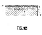
- a second SiO 2 layer 7 is formed on the PSG layer 6 by a plasma CVD method (see Fig.
- a second Si 3 N 4 layer 8 reaching the etching-stop layer 5 is formed all over a surface thereof by the plasma CVD method (see Fig. 33).
- a liquid supply port 9 extending from the rear surface side of the silicon substrate 1 to the sacrificial layer 4 is formed by the anisotropic etching (see Fig. 34).
- Japanese Patent Application Laid-open No. 2003-136492 discloses that if the sacrificial layer is formed of polysilicon by the same process as a filmforming process or an etching process for a gate electrode of a MOS transistor in a drive circuit or others, an exclusive mask for the sacrificial layer becomes unnecessary.
- the PSG layer may be dissolved by an etching liquid when the PSG layer is provided on a wiring layer such as a gate electrode, there is a case that it is unsuitable as an anti-etching layer.
- an etching liquid when a predetermined portion of the PSG layer 6 is etched as one of processes shown in Figs. 32 to 33 for supplying the liquid fed from a lower part of the substrate via the liquid supply port 9 to an upper part of the substrate, the sacrificial layer 4 is directly exposed to the etching liquid unless the etching-stop layer 5 covering the sacrificial layer 4 is separately provided.
- the etching-stop layer 5 formed of Si 3 N 4 is provided between the sacrificial layer 4 and the PSG layer 6. Accordingly, in a case wherein the PSG layer is provided on the wiring electrode, an anti-etching layer of silicon nitride used as the etching-stop layer is formed in a structure around the liquid supply port before the PSG layer is provided, so that the etching of the PSG layer is possible without affecting the sacrificial layer of polysilicon.
- the anti-etching layer of silicon nitride must be heated at a predetermined temperature when formed by the reduced pressure CVD method, polysilicon is used for the sacrificial layer formed together with the wiring layer in the same process.
- An object of the present invention is to provide a method for manufacturing a liquid-ejection head high in accuracy and in reliability while simplifying the manufacturing process thereof, wherein, prior to forming a liquid supply port passing through an insulating layer by the etching starting from a rear surface side of a substrate, a sacrificial layer in which the etching proceeds faster than in the substrate is formed on a surface of the substrate at a position corresponding to the liquid supply port and an etching-stop layer for interrupting the progress of the etching is formed in contact at least with the upper surface of the sacrificial layer.
- a separate process for forming the sacrificial layer is eliminated but such a process for manufacturing the sacrificial layer is carried out simultaneously with a process for forming an electrode wiring section, and the liquid supply head high in accuracy and in reliability is obtainable.
- the sacrificial layer may be formed of by using the same material, as that of the electrode wiring section, for example a material mainly composed of aluminum.
- the manufacturing processes may be reduced while the uniformity of sacrificial layers may be maintained in the respective substrates.
- the material forming the insulating layer may be silicon oxide and that forming the protective layer may be silicon nitride. In this case, even if the anti-etching layer is formed in a film state, the reliability thereof is still high to further enhance the yield during the anisotropic etching.
- the driver element may be a transistor, and the electrode wiring section may include a source and a drain of the transistor.
- the anti-etching layer may be formed to encircle the upper surface and the side surface of the sacrificial layer, further may be formed by using the same material as that of the insulating layer or the protective layer and at the same step as that for forming the insulating layer or the protective layer.
- the anti-etching layer may be formed by the plasma CVD method so as to have a residual stress of 3 ⁇ 10 8 dyn/cm 2 or less.
- the anti-etching layer may be formed by the plasma CVD method so that a tensile stress and a compressive stress are residual in a double-layered structure.
- the ejection energy generating section may have an electro-thermal transducer for generating thermal energy for ejecting liquid from the ejection opening by generating the film boiling in the liquid.
- the liquid ejection head further has an upper plate member formed above the insulating layer of the substrate to define a liquid chamber between the upper plate member and the insulating layer and having the ejection opening communicated with the liquid chamber
- the method according to the present invention may further comprise the steps of forming a first resinous layer having a shape corresponding to the liquid chamber on the protective layer, forming a second resinous layer having a shape corresponding to the upper plate member on the first resinous layer, removing a portion of the second resinous layer corresponding to the ejection opening from the second resinous layer, and removing the first resinous layer after the upper plate member has been formed.
- One feature of the present invention is to use a material mainly composed of aluminum for the wiring provided in a layer disposed above the sacrificial layer and the PSG layer and that disposed beneath the heat-generation resistive layer.
- the sacrificial layer is formed of the same material as the wiring material provided above the PSG layer and beneath the heat-generation resistive layer.
- the wiring material mainly composed of aluminum includes aluminum of 100% fineness, a so-called Al-Si alloy containing silicon in a range from 1 to 5% in aluminum or Al-Cu alloy containing copper in aluminum.
- FIG. 1 A structure of a printing element substrate 10 in a printing head according to a first embodiment is shown in Fig. 1.
- ejection energy generators, liquid chambers, ejection openings or others are formed on a silicon substrate 11 of 0.5 to 1 mm thick.
- a liquid supply port 12 of an elongate hole shape is formed to pass through the same.
- a plurality of electro-thermal transducers 13 are arranged at a predetermined gap in a lengthwise direction of the liquid supply port 12 while shifting half a pitch from one on the opposite side, whereby the ejection energy generator is constituted.
- electrode terminals 14 for electrically connecting the electro-thermal transducers 13 to a printer body and electric wiring not shown made, for example, of aluminum, both of which are formed by the deposition technique.
- a drive signal is input from a driving IC not shown to the electro-thermal transducer 13 via these electrode terminals 14, and simultaneously therewith, a driving power is supplied to the electro-thermal transducers 13.
- an upper plate member 17 having a plurality of ejection openings 16 confronting the electro-thermal transducers 13, respectively, via the liquid chambers 15. That is, a liquid path 18 for communicating the liquid supply port 12 with the individual liquid chambers 15 is formed between the upper plate member 17 and the silicon substrate 11, all of which are formed together with the upper plate member 17 by a lithographic technique in the same manner as the ejection openings 16.
- Liquid supplied from the liquid supply port 12 to the respective liquid chamber 15 boils by the heat generation of the electro-thermal transducer 13 when a drive signal is input to the electro-thermal transducer 13 in the corresponding liquid chamber 15, and is ejected from the ejection opening 16 by the pressure of bubbles generated thereby.
- a process for manufacturing such a printing element substrate 10 will be described with reference to Figs. 2 to 9.
- a P-type silicon substrate 11 of 625pm thick having the crystalline face orientation of ⁇ 100> is prepared, which surface is then heat-oxidized to form a SiO 2 layer 19 of 0.01 to 0.05 ⁇ m thick (corresponding to reference numeral 2 in Fig. 27).
- a Si 3 N 4 layer of 0.1 to 0.3 ⁇ m is deposited thereon by the reduced CVD method, and patterned so that this Si 3 N 4 layer 3 is left solely in a region in which a sacrificial layer 20 described later is formed (see Fig. 28).
- a source 21, a drain 22 and a gate electrode 23 are formed of polysilicon.
- the source 21 and the drain 22 are formed on the underside of the SiO 2 layer 19 by accelerating arsenic ions to pass through the SiO 2 layer 19 and be implanted at a predetermined position in the silicon substrate 11 by the ion implantation method, after which the silicon substrate 11 is heat-treated to diffuse arsenic ions in the silicon substrate 11, and the gate electrode 23 is formed on the SiO 2 layer 19 by the patterning (see Fig. 2).
- contact openings 24 for the source electrode 21 and the drain electrode 22 of the drive transistor are formed by the patterning and etching of the SiO 2 layer 19.
- an opening 25 is formed in a portion of the SiO 2 layer 19 in which the sacrificial layer 20 is to be formed in the same manner as above (see Fig. 3). A surface of the silicon substrate 11 is exposed to the opening 25.
- an electrode wiring layer 26 is formed of an electro-conductive material mainly composed of aluminum, such as Al-Si, for electrically connecting the electrode wiring layer 26 to the contact openings 24 by the patterning, whereby the drive transistor for driving the electro-thermal transducer 13 is completed.
- the sacrificial layer 20 using the same material as the electrode wiring layer 26 is formed in the opening 25. Since the same material as the electrode wiring layer 26 is used for forming the sacrificial layer 20, the latter is formed simultaneously with the former in the same process as forming the electrode wiring layer 26, whereby it is possible to eliminate an independent process for forming the sacrificial layer 20.
- an insulating layer 27 of SiO 2 of 1.0 to 1.8 ⁇ m thick is deposited on them by the plasma CVD method.
- This insulating layer 27 is an inter-layer film for the electrode wiring layer 26.
- first through-holes 28 are carried out from a surface of the insulating layer 27.
- a depth of the through-hole 28 is selected not to reach the electrode wiring layer 26 and the sacrificial layer 20.
- those formed opposite to the electrode wiring layer 26 electrically connected with the drain electrode 22 of the drive transistor and opposite to the sacrificial layer 20 are subjected to the patterning and the etching of second through-holes 29 to expose the electrode wiring layer 26 electrically connected to the drain electrode 22 and the sacrificial layer 20.
- a surface treatment layer 31 for an embedded wiring layer 30 and an etching-stop layer 32 are formed of the same material as the electro-thermal transducer 13, such as TaN or TaSi 3 N 4 on the inner wall of the first through-hole 29 and the second through-hole 28 and on the surface of the electrode wiring layer 26 and the sacrificial layer 20 exposed to the through-hole 29 by the sputtering.
- the surface treatment layer 31 and the etching-stop layer 32 are provided for facilitating the adhesive property to the insulating layer 27, they are operable, when the embedded wiring layer 30 and an embedded layer 33 are formed, for example, of copper by the electrolytic plating, also as an electrode therefore.
- the embedded wiring layer 30 and the embedded layer 33 may be formed of aluminum or the like by the sputtering.
- the etching-stop layer 32 can be formed of the same material as the surface treatment layer 31 as described above, the etching-stop layer 32 and the surface treatment layer 31 are simultaneously formed by the same process to eliminate an independent process for forming the etching-stop layer 32.
- a film of TaN or TaSi 3 N 4 having a thickness of 0.02 to 0.2 ⁇ m which is to be the electro-thermal transducer 13 is formed while striding over the embedded layer 33 by the patterning.
- a first protective layer 35 is formed of Si 3 N 4 by the plasma CVD method, and a second protective layer 36 is formed by the patterning while covering the electro-thermal transducer 13 via the first protective layer 35 (see Fig. 6).
- a resin (not shown) to be an anisotropic etching mask is coated on the rear surface of the silicon substrate 11 and processed to have a desired pattern by the lithography.
- the process proceeds to the formation of the upper plate 17, wherein a resist to be a core 37 for forming the liquid path 18 and the liquid chambers 15 is coated on the surface and patterned to have a predetermined shape.
- photosensitive epoxy resin to be the upper plate member 17 is coated on the core 37 and patterned to form the ejection openings 16 by the photolithography.
- the liquid supply port 12 reaching the sacrificial layer 20 is formed by the etching carried out on the rear surface of the silicon substrate 11, while using TMAH as the anisotropic etching liquid.
- This etching proceeds from the rear surface of the silicon substrate 11 at an angle of 55 degrees and reaches the sacrificial layer 20 encircled by the SiO 2 layer 19 and the etching-stop layer 32. Since the sacrificial layer 20 is isotropically etched by this etching liquid, the liquid supply port 12 has an upper end shaped in correspondence to the sacrificial layer 20 and widening toward the rear surface of the silicon substrate 11 in a tapered manner.
- the printing element substrate 10 is manufactured (see Fig. 9).
- the printing element substrate 10 when the printing element substrate 10 is manufactured, it is unnecessary to add a new process for forming the sacrificial layer 20 and the etching-stop layer 32, whereby the manufacturing process is simplified to suppress the increase in production cost and reduce a cycle time as well as the liquid supply port 12 is precisely formed.
- the sacrificial layer 20 when the sacrificial layer 20 is etched to form the liquid supply port 12, there is a possibility in that a portion of the insulating layer 27 adjacent to the sacrificial layer 20 is etched by the etching liquid and it is difficult to maintain the liquid supply port 12 at a desired dimension. Accordingly, to avoid such an inconvenience, the sacrificial layer 20 may be covered with the etching-stop layer 32.
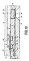
- a second embodiment of the present invention will be described with reference to Figs. 10 to 13, wherein parts having the same functions as in the preceding embodiment are indicated by the same reference numerals and the redundant explanation thereof are eliminated. That is, while the etching-stop layer 32 is solely brought into contact with the upper end surface of the sacrificial layer 20 in the preceding embodiment, the etching-stop layer 32 extends to the SiO 2 layer 19 to cover the sacrificial layer 20 according to this embodiment (see Fig. 10). Thereby, it is possible to completely shut the insulating layer 27 from the sacrificial layer 20.
- the etching-stop layer 32 and the embedded layer 33 are removed, and then a portion of the first protective layer 35 exposed to the liquid supply port 12 is removed by the dry etching (see Fig. 12). Further, the core 37 is removed by the etching to complete the printing element substrate 10 (see Fig. 13).
- the etching-stop layer 32 is formed simultaneously with the film formation of the surface treatment layer 31 by using the same material as the latter. However, if it is unnecessary to form the surface treatment layer 31, the etching-stop layer 32 may be formed of the same material as the embedded wiring layer 30 simultaneously with the formation of the latter.
- the electrode wiring layer 26 of aluminum-copper alloy (see Fig. 4) is formed on the PSG layer 38 and patterned to have a predetermined shape.
- the driver elements such as a drive transistor or others described hereinabove is completed.
- the SiO 2 insulating layer 27 of 1.0 to 1.8 ⁇ m thick is deposited by the plasma CVD method and patterned to have a predetermined shape (see Fig. 15).
- the TaN electro-thermal transducer 13 (see Fig. 6) of 0.02 to 0.1 ⁇ m thick and the aluminum-copper alloy electrode layer not shown of 0.1 to 0.8 ⁇ m are consecutively deposited on the insulating layer 27 and patterned to have a predetermined shape.
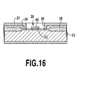
- a double-layered sacrificial layer 20 consisting of the electro-thermal transducer 13 and the electrode layer 40 is formed of the same material in the opening 39 (see Fig. 16).
- the protective layer 35 (see Fig. 6) is formed of Si 3 N 4 by the plasma etching method. Since this protective layer 35 has a function of the etching-stop layer 32, the residual stress thereof is reduced, for example, to 3 ⁇ 10 8 dyn/cm 2 or lower.
- the protective layer 35 thus formed is unsuitable for the protective layer for the electro-thermal transducer in view of the film quality or the step-coverage property, it may be formed as a double-layered structure having both of the tensile stress and compressive stress so that it satisfies the function of the protective layer 35 as well as the performance of the etching-stop layer 32.
- the etching-stop layer 32 of 0.4 ⁇ m thick is formed by the plasma CVD method, a first layer of 0.2 ⁇ m thick excellent in the tensile stress is first formed, and then a second layer of 0.2 ⁇ m excellent in the compressive stress is formed (see Fig. 17).
- While conditions for depositing this etching-stop layer 32 are different in accordance with the performance of the plasma CVD apparatus, it may be possible to change the internal residual stress from the tensile stress to the compressive stress, for example, by regulating the electric power applied to the silicon substrate 11. That is, since the internal residual stress left in the etching-stop layer 32 is adjustable solely by changing the deposition conditions while leaving the silicon substrate 11 within the plasma CVD apparatus, it is unnecessary to add a new process.
- a resin to be a mask for the anisotropic etching is coated on the rear surface of the silicon substrate 11 and patterned to have a predetermined shape.
- the anisotropic etching is carried out on the rear surface of the silicon substrate 11 by using TMAH to form the liquid supply port 12 reaching the sacrificial layer 20 (see Fig. 18). In this case, there is no bulge or crack in the etching-stop layer 32 after the etching has been stopped.
- the etching-stop layer 32 is removed by the dry etching, and further the core 37 (see Fig. 7) is removed.
- the electrode wiring layer 26 may be used as the sacrificial layer 20.
- the embodiment described here is the steps of manufacturing the printed substrate in which the electrode wiring layer 26 is simultaneously provided in the same process as that of the sacrificial layer 20 above the PSG layer 38 (after forming the same) and below the electro-thermal transducer 13, i.e. a heat-generation resistive layer 41 (before forming the same), and the wiring layer is formed in the same process as that of the sacrificial layer after the patterning of the PSG layer described above.
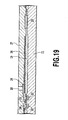
- the first through-hole 28 is formed on the surface of the insulating layer 27 by the patterning (see Fig. 19).
- the heat-generation resistive layer 41 is formed by the TaN sputtering, and an electrode layer 42 electrically connected to the heat-generating resistor is formed thereon (see Fig. 20).
- the electrode wiring layer 26 electrically connected to the electrode layer 42 via the heat-generation resistive layer 41 possessing electrical conductivity.
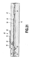
- the electrode layer 42 and the heat-generation resistive layer 41 are modified to a predetermined pattern by the patterning to form a heat-generating resistor section 43 (see Fig. 21).
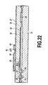
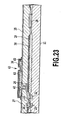
- a first protective layer 35 also behaving as an etching-stop layer is formed of Si 3 N 4 by the plasma CVD method (see Fig. 22), and a second protective layer 36 is formed to cover the heat-generating resistor section 43 via the first protective layer 35 by the patterning (see Fig. 23).
- a resin (not shown) to be a mask for the anisotropic etching is coated on the rear surface of the silicon substrate 11, and formed at a desired pattern by the lithography.
- the process proceeds to the formation of the upper plate member 17, wherein a resist to be a core 37 for forming a liquid flow path 18 and a liquid chamber 15 is coated on the surface and patterned to have a predetermined shape.
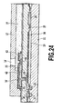
- a photosensitive epoxy resin to be the upper plate member 17 is coated on the core 37 and patterned to have a predetermined shape by the photolithography to form the ejection opening 16 (see Fig. 24).
- TMAH is used as the anisotropic etching liquid to etch the silicon substrate 11 from the rear surface thereof, thus forming the liquid supply port 12 reaching the sacrificial layer 20.
- This etching progresses from the rear surface of the silicon substrate 11 at an angle of 55.7 degrees to the sacrificial layer 20 encircled by the SiO 2 layer 19. Since the sacrificial layer 20 is isotropically etched with the etching liquid, the liquid supply port 12 has a shape corresponding to that of the sacrificial layer 20 at an upper end thereof and widening toward the rear surface of the silicon substrate 11 in a tapered manner (see Fig. 25).
- the core 37 is further removed by the etching.
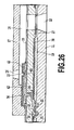
- the printing element substrate 10 is completed (see Fig. 26).
- the sacrificial layer in which the etching progresses faster than in the substrate and the etching-stop layer brought into contact with at least an upper surface of the sacrificial layer, for stopping the progress of the etching are formed in advance at a position for forming the liquid supply port.
- the process for forming the sacrificial layer is carried out simultaneously with the process for forming the electrode wiring section.
- the etching-stop layer is formed of the same material and by the same process for the insulating layer and the protective layer, an independent process for forming the etching-stop layer could be completely eliminated as well as the protective layer for this etching-stop layer is unnecessary, whereby the manufacturing process could be further simplified.
- the sacrificial layer could be formed of a material mainly composed of aluminum capable of being isotropically etched, whereby it is possible to carry out the process for forming the sacrificial layer simultaneously with that for forming the electrode wiring section.
Landscapes
- Engineering & Computer Science (AREA)
- Manufacturing & Machinery (AREA)
- Particle Formation And Scattering Control In Inkjet Printers (AREA)
- Micromachines (AREA)
Abstract
Description
- The present invention relates to a method for manufacturing a liquid ejection head capable of simplifying the manufacturing process and excellent in reliability.
- In this Specification, a word "print" refers to not only forming a significant information, such as characters and figures, but also forming images, designs or patterns on a printing medium and processing such as etching and so forth in the printing medium, whether the information is significant or insignificant or whether it is visible so as to be perceived by humans. The term "printing medium" includes not only paper used in common printing apparatus, but also sheet materials such as cloths, plastic films, metal sheets, glass plates, ceramic sheets, wood panels and leathers or three-dimensional materials such as spheres, round pipes and so forth which can receive the ink. The word "ink" should be interpreted in its wide sense as with the word "print", refers to liquid that is applied to the printing medium for forming images, designs or patterns, processing such as etching in the printing medium or processing such as coagulating or insolubilizing a colorant in the ink and includes any liquids used for printing.
- As a conventional art, an ink-jet printing method disclosed in Japanese Patent Application Laid-open No. 54-51835(1979) is characterized in that a driving force for ejecting a liquid droplet is obtained by applying a thermal energy to the liquid, which is different from other ink-jet printing methods. That is, according to this ink-jet printing method, the liquid subjected to the operation of the thermal energy is vaporized to generate air bubbles. The expansion force accompanied with the growth of the bubbles makes liquid droplets to be ejected from an orifice of a printing head to a printing medium so that a predetermined image information such as characters or images is printed on the printing medium. The printing head used for this ink-jet printing method generally includes an nozzle orifice for ejecting the liquid, a liquid chamber communicating with the nozzle orifice, for storing the liquid to be ejected, an ejection energy generator disposed in the liquid chamber, for generating the thermal energy for ejecting the liquid droplet from the nozzle orifice, a protecting layer for protecting the ejection energy generator from the liquid, and a heat storage layer for storing the thermal energy generated from the ejection energy generator.
- Also, in Japanese Patent Application Laid-open No. 10-13849(1998), a method is disclosed, for forming, by an anisotropic etching, a liquid supply port communicating with the above-mentioned liquid chamber to supply the liquid to this liquid chamber. In Japanese Patent Application Laid-open No. 10-181032(1998), a method is disclosed, for forming the liquid supplying port more precisely by further using a sacrificial layer. In this Japanese Patent Application Laid-open No. 10-181032(1998), a concrete process performed by the sacrificial layer during the high-precision etching is described in the explanation of a first embodiment with reference to Figs. 1 to 3.
- One example of a process for manufacturing the liquid supply port in the conventional printing head described above will be described with reference to Figs. 27 to 34 based on the technique disclosed in Japanese Patent Application Laid-open No. 10-181032(1998) as follows. A SiO2 layer 2 is formed by oxidizing the surface of a
silicon substrate 1 and deposits a Si3N4 layer 3 thereon by a reduced pressure CVD method (see Fig. 27). Then, a patterning is carried out to leave the Si3N4 layer 3 solely in the vicinity of a region in which a sacrificial layer 4 described later is formed. At this time, all of the Si3N4 layer 3 deposited on the rear surface of the silicon substrate is removed by the etching during the patterning (see Fig. 28). Next, thesilicon substrate 1 is further heat-oxidized to grow the SiO2 layer 2. At this time, a portion disposed directly beneath the patterned Si3N4 layer 3 is not oxidized but solely the SiO2 layer 2 disposed on the opposite sides thereof is selectively oxidized, whereby a thickness of the SiO2 layer 2 not covered with the Si3N4 layer 3 increases. Thereafter, the Si3N4 layer 3 is removed by the etching (see Fig. 29). Then, to form a sacrificial layer 4 of polysilicon, a portion of the SiO2 layer 2 having a thin film thickness because this portion has been covered with the Si3N4 layer 3 is removed by the etching, and instead, the sacrificial layer 4 of polysilicon is formed in this portion (see Fig. 30). Next, an etching-stop layer 5 encircling this sacrificial layer 4 is formed of Si3N4 which stress is adjusted by the reduced pressure CVD method, and a whole surface thereof is covered with a phosphosilicate glass (PSG) layer 6 (see Fig. 31). Further, a second SiO2 layer 7 is formed on thePSG layer 6 by a plasma CVD method (see Fig. 32), and the SiO2 layer 7 and thePSG layer 6 are patterned, after which a second Si3N4 layer 8 reaching the etching-stop layer 5 is formed all over a surface thereof by the plasma CVD method (see Fig. 33). Thereafter, a liquid supply port 9 extending from the rear surface side of thesilicon substrate 1 to the sacrificial layer 4 is formed by the anisotropic etching (see Fig. 34). - Japanese Patent Application Laid-open No. 2003-136492 discloses that if the sacrificial layer is formed of polysilicon by the same process as a filmforming process or an etching process for a gate electrode of a MOS transistor in a drive circuit or others, an exclusive mask for the sacrificial layer becomes unnecessary.
- However, since a resistivity of polysilicon is generally high, it is necessary to lower the resistivity when used as the gate electrode of the transistor, for example, by doping impurity. On the other hand, since an etching speed of polysilicon doped with impurity is liable to lower, it is unsuitable for using polysilicon as a material for the sacrificial layer which needs the etching speed higher than that of a material to be etched. Accordingly, when the electrode and the sacrificial layer are formed of the same material; polysilicon; for the purpose of saving the manufacturing process, one or both of the electrode and the sacrificial layer may be lower in performance, whereby it is impossible to merely use the polysilicon as it is.
- Further, since the PSG layer may be dissolved by an etching liquid when the PSG layer is provided on a wiring layer such as a gate electrode, there is a case that it is unsuitable as an anti-etching layer. For example, when a predetermined portion of the
PSG layer 6 is etched as one of processes shown in Figs. 32 to 33 for supplying the liquid fed from a lower part of the substrate via the liquid supply port 9 to an upper part of the substrate, the sacrificial layer 4 is directly exposed to the etching liquid unless the etching-stop layer 5 covering the sacrificial layer 4 is separately provided. - In the prior art, to avoid such a problem, the etching-
stop layer 5 formed of Si3N4 is provided between the sacrificial layer 4 and thePSG layer 6. Accordingly, in a case wherein the PSG layer is provided on the wiring electrode, an anti-etching layer of silicon nitride used as the etching-stop layer is formed in a structure around the liquid supply port before the PSG layer is provided, so that the etching of the PSG layer is possible without affecting the sacrificial layer of polysilicon. - Also, since the anti-etching layer of silicon nitride must be heated at a predetermined temperature when formed by the reduced pressure CVD method, polysilicon is used for the sacrificial layer formed together with the wiring layer in the same process.
- Accordingly, in the conventional structure, there has been no method for manufacturing a liquid ejection head capable of reducing the manufacturing processes while maintaining the uniformity of sacrificial layers in the respective substrates taken from the same wafer.
- An object of the present invention is to provide a method for manufacturing a liquid-ejection head high in accuracy and in reliability while simplifying the manufacturing process thereof, wherein, prior to forming a liquid supply port passing through an insulating layer by the etching starting from a rear surface side of a substrate, a sacrificial layer in which the etching proceeds faster than in the substrate is formed on a surface of the substrate at a position corresponding to the liquid supply port and an etching-stop layer for interrupting the progress of the etching is formed in contact at least with the upper surface of the sacrificial layer.
- To achieve the above-mentioned object, a method for manufacturing a liquid ejection head according to the present invention having a substrate including an ejection energy generating section for ejecting a liquid from an ejection opening, a driver element provided as a lower layer of the ejection energy generating section via an insulating layer for driving the ejection energy generating section, an electrode wiring section electrically connecting the driver element to the ejection energy generating section, formed of a material mainly composed of aluminum, a protective layer formed on the insulating layer to cover the ejection energy generating section, and a liquid supply port therethrough, comprises the steps of forming a sacrificial layer at a position at which the liquid supply port is to be formed, by using the same material as that of the electrode wiring section, when the electrode wiring section is formed, forming an anti-etching layer for covering the sacrificial layer, having the durability against an etching liquid, etching the substrate with the etching liquid from a surface of the substrate on which the ejection energy generating section is formed until the sacrificial layer is exposed, further proceeding the etching to remove the sacrificial layer and expose a portion of the anti-etching layer to be the liquid supply port, and forming the liquid supply port in the substrate by removing the exposed anti-etching layer.
- According to the present invention, a separate process for forming the sacrificial layer is eliminated but such a process for manufacturing the sacrificial layer is carried out simultaneously with a process for forming an electrode wiring section, and the liquid supply head high in accuracy and in reliability is obtainable.
- In the method for manufacturing the liquid ejection head according to the present invention, the sacrificial layer may be formed of by using the same material, as that of the electrode wiring section, for example a material mainly composed of aluminum. In this case, the manufacturing processes may be reduced while the uniformity of sacrificial layers may be maintained in the respective substrates.
- The material forming the insulating layer may be silicon oxide and that forming the protective layer may be silicon nitride. In this case, even if the anti-etching layer is formed in a film state, the reliability thereof is still high to further enhance the yield during the anisotropic etching.
- The driver element may be a transistor, and the electrode wiring section may include a source and a drain of the transistor.
- The anti-etching layer may be formed to encircle the upper surface and the side surface of the sacrificial layer, further may be formed by using the same material as that of the insulating layer or the protective layer and at the same step as that for forming the insulating layer or the protective layer. In this case, the anti-etching layer may be formed by the plasma CVD method so as to have a residual stress of 3×10⁸ dyn/cm2 or less. Alternatively, the anti-etching layer may be formed by the plasma CVD method so that a tensile stress and a compressive stress are residual in a double-layered structure.
- The ejection energy generating section may have an electro-thermal transducer for generating thermal energy for ejecting liquid from the ejection opening by generating the film boiling in the liquid.
- The liquid ejection head further has an upper plate member formed above the insulating layer of the substrate to define a liquid chamber between the upper plate member and the insulating layer and having the ejection opening communicated with the liquid chamber, the method according to the present invention may further comprise the steps of forming a first resinous layer having a shape corresponding to the liquid chamber on the protective layer, forming a second resinous layer having a shape corresponding to the upper plate member on the first resinous layer, removing a portion of the second resinous layer corresponding to the ejection opening from the second resinous layer, and removing the first resinous layer after the upper plate member has been formed.
- One feature of the present invention is to use a material mainly composed of aluminum for the wiring provided in a layer disposed above the sacrificial layer and the PSG layer and that disposed beneath the heat-generation resistive layer.
- In the present invention, it is possible to use aluminum as a material for forming the sacrificial layer and the wiring layer, but impossible to use polysilicon as a material for forming the sacrificial layer and the wiring layer. Reasons therefore are the following four points:
- 1. Since polysilicon is generally high in resistivity, it is necessary to lower the resistivity, for example, by doping impurity therein if the polysilicon is used as a wiring resistive layer for a gate electrode in a transistor.
- 2. Regarding the sacrificial layer, when tetramethylammonium hydroxide (TMAH) is used as an anisotropic etching liquid, an isotropic etching speed of a material to be mainly etched by TMAH must be higher than the anisotropic etching speed thereof. However, when the impurity is doped, the former etching speed is liable to lower.
- 3. Due to the above-mentioned
reasons - 4. Since the aluminum is low in resistivity and high in etching speed by the anisotropic etching liquid TMAH, even if both of the wiring layer and the sacrificial layer are formed of aluminum, the performance thereof is not lowered.
- According to the present invention, the sacrificial layer is formed of the same material as the wiring material provided above the PSG layer and beneath the heat-generation resistive layer. Reasons therefore are the following two points;
- 1. The control of the operation under the severe condition is necessary for etching the PSG layer without etching the polysilicon sacrificial layer since there is the PSG layer unsuitable for the anti-etching mask above the wiring layer which becomes the gate electrode. Especially, when the operation is carried out for cutting a number of substrates out from a single wafer, it is very difficult to leave the sacrificial layers in the respective substrates while maintaining the uniform shape.
- 2. Since the material for the heat-generation resistive layer functions as an anti-etching layer, a novel patterning process is necessary wherein the material is not left beneath the sacrificial layer.
- In this regard, according to the present invention, the wiring material mainly composed of aluminum includes aluminum of 100% fineness, a so-called Al-Si alloy containing silicon in a range from 1 to 5% in aluminum or Al-Cu alloy containing copper in aluminum.
- The above and other objects, effects, features and advantages of the present invention will become more apparent from the following description of embodiments thereof taken in conjunction with the accompanying drawings.
- Fig. 1 is a perspective view of an appearance of a printing element substrate constituting a main part of a printing head according to a first embodiment of the present invention;
- Fig. 2 is a sectional view of the printing element substrate representing a process for manufacturing the printing head according to the first embodiment of the present invention;
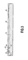
- Fig. 3 is a sectional view of the printing element substrate representing a process for manufacturing the printing head according to the first embodiment of the present invention;
- Fig. 4 is a sectional view of the printing element substrate representing a process for manufacturing the printing head according to the first embodiment of the present invention;
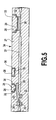
- Fig. 5 is a sectional view of the printing element substrate representing a process for manufacturing the printing head according to the first embodiment of the present invention;
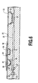
- Fig. 6 is a sectional view of the printing element substrate representing a process for manufacturing the printing head according to the first embodiment of the present invention;
- Fig. 7 is a sectional view of the printing element substrate representing a process for manufacturing the printing head according to the first embodiment of the present invention;
- Fig. 8 is a sectional view of the printing element substrate representing a process for manufacturing the printing head according to the first embodiment of the present invention;
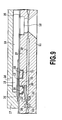
- Fig. 9 is a sectional view of the printing element substrate representing a process for manufacturing the printing head according to the first embodiment of the present invention;
- Fig. 10 is a sectional view of a printing element substrate representing a process for manufacturing a printing head according to a second embodiment of the present invention;
- Fig. 11 is a sectional view of the printing element substrate representing a process for manufacturing the printing head according to the second embodiment of the present invention;
- Fig. 12 is a sectional view of the printing element substrate representing a process for manufacturing the printing head according to the second embodiment of the present invention;
- Fig. 13 is a sectional view of the printing element substrate representing a process for manufacturing the printing head according to the second embodiment of the present invention;
- Fig. 14 is a sectional view of a printing element substrate representing a process for manufacturing a printing head according to a third embodiment of the present invention;
- Fig. 15 is a sectional view of the printing element substrate representing a process for manufacturing the printing head according to the third embodiment of the present invention;
- Fig. 16 is a sectional view of the printing element substrate representing a process for manufacturing the printing head according to the third embodiment of the present invention;
- Fig. 17 is a sectional view of the printing element substrate representing a process for manufacturing the printing head according to the third embodiment of the present invention;
- Fig. 18 is a sectional view of the printing element substrate representing a process for manufacturing the printing head according to the third embodiment of the present invention;
- Fig. 19 is a sectional view of a printing element substrate representing a process for manufacturing a printing head according to a fourth embodiment of the present invention;
- Fig. 20 is a sectional view of the printing element substrate representing a process for manufacturing the printing head according to the fourth embodiment of the present invention;
- Fig. 21 is a sectional view of the printing element substrate representing a process for manufacturing the printing head according to the fourth embodiment of the present invention;
- Fig. 22 is a sectional view of the printing element substrate representing a process for manufacturing the printing head according to the fourth embodiment of the present invention;
- Fig. 23 is a sectional view of the printing element substrate representing a process for manufacturing the printing head according to the fourth embodiment of the present invention;
- Fig. 24 is a sectional view of the printing element substrate representing a process for manufacturing the printing head according to the fourth embodiment of the present invention;
- Fig. 25 is a sectional view of the printing element substrate representing a process for manufacturing the printing head according to the fourth embodiment of the present invention;
- Fig. 26 is a sectional view of the printing element substrate representing a process for manufacturing the printing head according to the fourth embodiment of the present invention;
- Fig. 27 is a sectional view representing a process for manufacturing the printing element substrate of a prior art printing head;
- Fig. 28 is a sectional view representing a process for manufacturing the printing element substrate of the prior art printing head;
- Fig. 29 is a sectional view representing a process for manufacturing the printing element substrate of the prior art printing head;
- Fig. 30 is a sectional view representing a process for manufacturing the printing element substrate of the prior art printing head;
- Fig. 31 is a sectional view representing a process for manufacturing the printing element substrate of the prior art printing head;
- Fig. 32 is a sectional view representing a process for manufacturing the printing element substrate of the prior art printing head;
- Fig. 33 is a sectional view representing a process for manufacturing the printing element substrate of the prior art printing head; and
- Fig. 34 is a sectional view representing a process for manufacturing the printing element substrate of the prior art printing head.
- While embodiments of the inventive method for manufacturing a liquid ejection head will be described below in detail with reference to Figs. 1 to 26, the present invention should not be limited to such embodiments but may be applicable to other techniques to be includes in a concept of the present invention defined by a scope of claim for patent.
- A structure of a
printing element substrate 10 in a printing head according to a first embodiment is shown in Fig. 1. In theprinting element substrate 10, ejection energy generators, liquid chambers, ejection openings or others are formed on asilicon substrate 11 of 0.5 to 1 mm thick. - In the
silicon substrate 11, aliquid supply port 12 of an elongate hole shape is formed to pass through the same. On opposite sides of theliquid supply port 12, a plurality of electro-thermal transducers 13 are arranged at a predetermined gap in a lengthwise direction of theliquid supply port 12 while shifting half a pitch from one on the opposite side, whereby the ejection energy generator is constituted. In thesilicon substrate 11, other than the electro-thermal transducers 13, there areelectrode terminals 14 for electrically connecting the electro-thermal transducers 13 to a printer body and electric wiring not shown made, for example, of aluminum, both of which are formed by the deposition technique. A drive signal is input from a driving IC not shown to the electro-thermal transducer 13 via theseelectrode terminals 14, and simultaneously therewith, a driving power is supplied to the electro-thermal transducers 13. - On the
silicon substrate 11, there is anupper plate member 17 having a plurality ofejection openings 16 confronting the electro-thermal transducers 13, respectively, via theliquid chambers 15. That is, aliquid path 18 for communicating theliquid supply port 12 with the individualliquid chambers 15 is formed between theupper plate member 17 and thesilicon substrate 11, all of which are formed together with theupper plate member 17 by a lithographic technique in the same manner as theejection openings 16. - Liquid supplied from the
liquid supply port 12 to the respectiveliquid chamber 15 boils by the heat generation of the electro-thermal transducer 13 when a drive signal is input to the electro-thermal transducer 13 in the correspondingliquid chamber 15, and is ejected from the ejection opening 16 by the pressure of bubbles generated thereby. - A process for manufacturing such a
printing element substrate 10 will be described with reference to Figs. 2 to 9. First, a P-type silicon substrate 11 of 625pm thick having the crystalline face orientation of <100> is prepared, which surface is then heat-oxidized to form a SiO2 layer 19 of 0.01 to 0.05 µm thick (corresponding to reference numeral 2 in Fig. 27). Further, a Si3N4 layer of 0.1 to 0.3 µm (corresponding to reference numeral 3 in Fig. 27) is deposited thereon by the reduced CVD method, and patterned so that this Si3N4 layer 3 is left solely in a region in which asacrificial layer 20 described later is formed (see Fig. 28). By the etching during this patterning, all of the Si3N4 layer 3 formed on the rear surface of thesilicon substrate 11 is removed. Thesilicon substrate 11 is again heat-oxidized in this state to grow the SiO2 layer 19 again so that the thickness thereof becomes 0.6 to 1.1 µm. At this time, since a portion of thesilicon substrate 11 directly beneath the SiO2 layer 19 covered with the patterned Si3N4 layer 3 is not so heat-oxidized, a region of thesilicon substrate 11 not interposed with the Si3N4 layer 3 is selectively oxidized to increase the film thickness more than that covered with the Si3N4 layer 3. Thereafter, the patterned Si3N4 layer 3 is removed by the etching (see Fig. 2). - Next, a
source 21, adrain 22 and agate electrode 23 are formed of polysilicon. In this case, thesource 21 and thedrain 22 are formed on the underside of the SiO2 layer 19 by accelerating arsenic ions to pass through the SiO2 layer 19 and be implanted at a predetermined position in thesilicon substrate 11 by the ion implantation method, after which thesilicon substrate 11 is heat-treated to diffuse arsenic ions in thesilicon substrate 11, and thegate electrode 23 is formed on the SiO2 layer 19 by the patterning (see Fig. 2). - Then, contact
openings 24 for thesource electrode 21 and thedrain electrode 22 of the drive transistor are formed by the patterning and etching of the SiO2 layer 19. Simultaneously, anopening 25 is formed in a portion of the SiO2 layer 19 in which thesacrificial layer 20 is to be formed in the same manner as above (see Fig. 3). A surface of thesilicon substrate 11 is exposed to theopening 25. - Next, an
electrode wiring layer 26 is formed of an electro-conductive material mainly composed of aluminum, such as Al-Si, for electrically connecting theelectrode wiring layer 26 to thecontact openings 24 by the patterning, whereby the drive transistor for driving the electro-thermal transducer 13 is completed. Simultaneously therewith, thesacrificial layer 20 using the same material as theelectrode wiring layer 26 is formed in theopening 25. Since the same material as theelectrode wiring layer 26 is used for forming thesacrificial layer 20, the latter is formed simultaneously with the former in the same process as forming theelectrode wiring layer 26, whereby it is possible to eliminate an independent process for forming thesacrificial layer 20. - Then, an insulating
layer 27 of SiO2 of 1.0 to 1.8 µm thick is deposited on them by the plasma CVD method. This insulatinglayer 27 is an inter-layer film for theelectrode wiring layer 26. - Next, the patterning and etching of first through-
holes 28 are carried out from a surface of the insulatinglayer 27. A depth of the through-hole 28 is selected not to reach theelectrode wiring layer 26 and thesacrificial layer 20. Of these first through-holes 28, those formed opposite to theelectrode wiring layer 26 electrically connected with thedrain electrode 22 of the drive transistor and opposite to thesacrificial layer 20 are subjected to the patterning and the etching of second through-holes 29 to expose theelectrode wiring layer 26 electrically connected to thedrain electrode 22 and thesacrificial layer 20. - Then, a
surface treatment layer 31 for an embeddedwiring layer 30 and an etching-stop layer 32 are formed of the same material as the electro-thermal transducer 13, such as TaN or TaSi3N4 on the inner wall of the first through-hole 29 and the second through-hole 28 and on the surface of theelectrode wiring layer 26 and thesacrificial layer 20 exposed to the through-hole 29 by the sputtering. While thesurface treatment layer 31 and the etching-stop layer 32 are provided for facilitating the adhesive property to the insulatinglayer 27, they are operable, when the embeddedwiring layer 30 and an embeddedlayer 33 are formed, for example, of copper by the electrolytic plating, also as an electrode therefore. Alternatively, the embeddedwiring layer 30 and the embeddedlayer 33 may be formed of aluminum or the like by the sputtering. - Since the etching-
stop layer 32 can be formed of the same material as thesurface treatment layer 31 as described above, the etching-stop layer 32 and thesurface treatment layer 31 are simultaneously formed by the same process to eliminate an independent process for forming the etching-stop layer 32. - After the embedded
wiring layer 30 and the embeddedlayer 33 have been simultaneously formed in the first through-hole 28 and the second through-hole 29 in which thesurface treatment layer 31 and the etching-stop layer 32 are formed, a whole surface is polished by a CMP method to form a flat surface 34 (see Fig. 5). - Next, a film of TaN or TaSi3N4 having a thickness of 0.02 to 0.2 µm which is to be the electro-
thermal transducer 13 is formed while striding over the embeddedlayer 33 by the patterning. Further, a firstprotective layer 35 is formed of Si3N4 by the plasma CVD method, and a secondprotective layer 36 is formed by the patterning while covering the electro-thermal transducer 13 via the first protective layer 35 (see Fig. 6). - Thereafter, to form the
liquid supply port 12 in thesilicon substrate 11, a resin (not shown) to be an anisotropic etching mask is coated on the rear surface of thesilicon substrate 11 and processed to have a desired pattern by the lithography. - Sequentially, the process proceeds to the formation of the
upper plate 17, wherein a resist to be a core 37 for forming theliquid path 18 and theliquid chambers 15 is coated on the surface and patterned to have a predetermined shape. - Then, photosensitive epoxy resin to be the
upper plate member 17 is coated on thecore 37 and patterned to form theejection openings 16 by the photolithography. - Next, the
liquid supply port 12 reaching thesacrificial layer 20 is formed by the etching carried out on the rear surface of thesilicon substrate 11, while using TMAH as the anisotropic etching liquid. This etching proceeds from the rear surface of thesilicon substrate 11 at an angle of 55 degrees and reaches thesacrificial layer 20 encircled by the SiO2 layer 19 and the etching-stop layer 32. Since thesacrificial layer 20 is isotropically etched by this etching liquid, theliquid supply port 12 has an upper end shaped in correspondence to thesacrificial layer 20 and widening toward the rear surface of thesilicon substrate 11 in a tapered manner. - Then, after the etching-
stop layer 32 and the embeddedlayer 33 have been removed by the etching, a portion of the firstprotective layer 35 exposed to theliquid supply port 12 is removed by the dry etching (see Fig. 8), and thecore 37 is removed by the etching. Thus, theprinting element substrate 10 is manufactured (see Fig. 9). - As described above, when the
printing element substrate 10 is manufactured, it is unnecessary to add a new process for forming thesacrificial layer 20 and the etching-stop layer 32, whereby the manufacturing process is simplified to suppress the increase in production cost and reduce a cycle time as well as theliquid supply port 12 is precisely formed. - In the above-mentioned embodiment, when the
sacrificial layer 20 is etched to form theliquid supply port 12, there is a possibility in that a portion of the insulatinglayer 27 adjacent to thesacrificial layer 20 is etched by the etching liquid and it is difficult to maintain theliquid supply port 12 at a desired dimension. Accordingly, to avoid such an inconvenience, thesacrificial layer 20 may be covered with the etching-stop layer 32. - Such a second embodiment of the present invention will be described with reference to Figs. 10 to 13, wherein parts having the same functions as in the preceding embodiment are indicated by the same reference numerals and the redundant explanation thereof are eliminated. That is, while the etching-
stop layer 32 is solely brought into contact with the upper end surface of thesacrificial layer 20 in the preceding embodiment, the etching-stop layer 32 extends to the SiO2 layer 19 to cover thesacrificial layer 20 according to this embodiment (see Fig. 10). Thereby, it is possible to completely shut the insulatinglayer 27 from thesacrificial layer 20. - Thus, in a state shown in Fig. 10, when the
liquid supply port 12 reaching thesacrificial layer 20 is formed by the anisotropic etching carried out on the rear surface of thesilicon substrate 11, the invasion of the etching liquid upon the insulatinglayer 27 is completely prevented since the insulatinglayer 27 is separated from thesacrificial layer 20 by the SiO2 layer 19 and the etching-stop layer 32 (see Fig. 11). - Thereafter, the etching-
stop layer 32 and the embeddedlayer 33 are removed, and then a portion of the firstprotective layer 35 exposed to theliquid supply port 12 is removed by the dry etching (see Fig. 12). Further, thecore 37 is removed by the etching to complete the printing element substrate 10 (see Fig. 13). - In the above-mentioned embodiment, the etching-
stop layer 32 is formed simultaneously with the film formation of thesurface treatment layer 31 by using the same material as the latter. However, if it is unnecessary to form thesurface treatment layer 31, the etching-stop layer 32 may be formed of the same material as the embeddedwiring layer 30 simultaneously with the formation of the latter. - Then, a third embodiment of the present invention is described with reference to Figs. 14 to 18. In this case, to avoid the redundancy, the
liquid supply port 12 will be solely described. In these drawings, parts having the same functions as in the preceding embodiments are indicated by the same reference numerals. That is, after the SiO2 layer 19 is formed on thesilicon substrate 11 and thePSG layer 38 is formed thereon by the cold CVD method, portions of the SiO2 layer 19 and thePSG layer 38 in which theliquid supply port 12 is to be formed are simultaneously removed by the etching to form anopening 39, to which is exposed the silicon substrate 11 (see Fig. 14). - Next, the
electrode wiring layer 26 of aluminum-copper alloy (see Fig. 4) is formed on thePSG layer 38 and patterned to have a predetermined shape. At this stage, the driver elements such as a drive transistor or others described hereinabove is completed. - Then, the SiO2 insulating layer 27 of 1.0 to 1.8 µm thick is deposited by the plasma CVD method and patterned to have a predetermined shape (see Fig. 15).
- Next, the TaN electro-thermal transducer 13 (see Fig. 6) of 0.02 to 0.1 µm thick and the aluminum-copper alloy electrode layer not shown of 0.1 to 0.8 µm are consecutively deposited on the insulating
layer 27 and patterned to have a predetermined shape. Simultaneously therewith, a double-layeredsacrificial layer 20 consisting of the electro-thermal transducer 13 and theelectrode layer 40 is formed of the same material in the opening 39 (see Fig. 16). - Then, the protective layer 35 (see Fig. 6) is formed of Si3N4 by the plasma etching method. Since this
protective layer 35 has a function of the etching-stop layer 32, the residual stress thereof is reduced, for example, to 3×10⁸ dyn/cm2 or lower. - If the
protective layer 35 thus formed is unsuitable for the protective layer for the electro-thermal transducer in view of the film quality or the step-coverage property, it may be formed as a double-layered structure having both of the tensile stress and compressive stress so that it satisfies the function of theprotective layer 35 as well as the performance of the etching-stop layer 32. Concretely, when the etching-stop layer 32 of 0.4µm thick is formed by the plasma CVD method, a first layer of 0.2µm thick excellent in the tensile stress is first formed, and then a second layer of 0.2µm excellent in the compressive stress is formed (see Fig. 17). - While conditions for depositing this etching-
stop layer 32 are different in accordance with the performance of the plasma CVD apparatus, it may be possible to change the internal residual stress from the tensile stress to the compressive stress, for example, by regulating the electric power applied to thesilicon substrate 11. That is, since the internal residual stress left in the etching-stop layer 32 is adjustable solely by changing the deposition conditions while leaving thesilicon substrate 11 within the plasma CVD apparatus, it is unnecessary to add a new process. - Thereafter, to form the
liquid supply port 12, a resin to be a mask for the anisotropic etching is coated on the rear surface of thesilicon substrate 11 and patterned to have a predetermined shape. - On the other hand, the formation of the
upper plate member 17 starts in the same manner as in the preceding embodiment (see Fig. 7). - Next, the anisotropic etching is carried out on the rear surface of the
silicon substrate 11 by using TMAH to form theliquid supply port 12 reaching the sacrificial layer 20 (see Fig. 18). In this case, there is no bulge or crack in the etching-stop layer 32 after the etching has been stopped. - Finally, the etching-
stop layer 32 is removed by the dry etching, and further the core 37 (see Fig. 7) is removed. - In such a manner, an independent process is unnecessary for forming the
sacrificial layer 20 and the etching-stop layer 32, whereby the liquid supply port having a favorable dimensional accuracy is obtainable without increasing the production cost of theprinting element substrate 10. - In the above-mentioned embodiment, while the electro-
thermal transducer 13 and theelectrode layer 40 are adopted as thesacrificial layer 20, theelectrode wiring layer 26 may be used as thesacrificial layer 20. - Then, a fourth embodiment of the inventive method for manufacturing a liquid ejection head will be described with reference to Figs. 19 to 24, wherein parts having the same function as in the preceding embodiment will be indicated by the same reference numerals.
- The embodiment described here is the steps of manufacturing the printed substrate in which the
electrode wiring layer 26 is simultaneously provided in the same process as that of thesacrificial layer 20 above the PSG layer 38 (after forming the same) and below the electro-thermal transducer 13, i.e. a heat-generation resistive layer 41 (before forming the same), and the wiring layer is formed in the same process as that of the sacrificial layer after the patterning of the PSG layer described above. - After the
printing element substrate 10 has been manufactured by the same process as in the first embodiment shown in Figs. 1 to 4, the first through-hole 28 is formed on the surface of the insulatinglayer 27 by the patterning (see Fig. 19). - Next, the heat-generation
resistive layer 41 is formed by the TaN sputtering, and anelectrode layer 42 electrically connected to the heat-generating resistor is formed thereon (see Fig. 20). Theelectrode wiring layer 26 electrically connected to theelectrode layer 42 via the heat-generationresistive layer 41 possessing electrical conductivity. Then, theelectrode layer 42 and the heat-generationresistive layer 41 are modified to a predetermined pattern by the patterning to form a heat-generating resistor section 43 (see Fig. 21). - A first
protective layer 35 also behaving as an etching-stop layer is formed of Si3N4 by the plasma CVD method (see Fig. 22), and a secondprotective layer 36 is formed to cover the heat-generatingresistor section 43 via the firstprotective layer 35 by the patterning (see Fig. 23). - Thereafter, for the purpose of forming the
liquid supply port 12, a resin (not shown) to be a mask for the anisotropic etching is coated on the rear surface of thesilicon substrate 11, and formed at a desired pattern by the lithography. - Subsequently, the process proceeds to the formation of the
upper plate member 17, wherein a resist to be a core 37 for forming aliquid flow path 18 and aliquid chamber 15 is coated on the surface and patterned to have a predetermined shape. - Then, a photosensitive epoxy resin to be the
upper plate member 17 is coated on thecore 37 and patterned to have a predetermined shape by the photolithography to form the ejection opening 16 (see Fig. 24). - Next, TMAH is used as the anisotropic etching liquid to etch the
silicon substrate 11 from the rear surface thereof, thus forming theliquid supply port 12 reaching thesacrificial layer 20. This etching progresses from the rear surface of thesilicon substrate 11 at an angle of 55.7 degrees to thesacrificial layer 20 encircled by the SiO2 layer 19. Since thesacrificial layer 20 is isotropically etched with the etching liquid, theliquid supply port 12 has a shape corresponding to that of thesacrificial layer 20 at an upper end thereof and widening toward the rear surface of thesilicon substrate 11 in a tapered manner (see Fig. 25). - Then, after the SiO2 layer 19 and the first
protective layer 35 have been removed by the etching, thecore 37 is further removed by the etching. Thus, theprinting element substrate 10 is completed (see Fig. 26). - According to such an embodiment, prior to forming the liquid supply port passing through the insulating layer by the etching starting from the rear surface of the substrate, the sacrificial layer in which the etching progresses faster than in the substrate and the etching-stop layer brought into contact with at least an upper surface of the sacrificial layer, for stopping the progress of the etching are formed in advance at a position for forming the liquid supply port. At this time, the process for forming the sacrificial layer is carried out simultaneously with the process for forming the electrode wiring section. Thus, it is possible to simplify the manufacturing process because an independent process for forming the sacrificial layer is eliminated. Particularly, when the sacrificial layer and the electrode wiring section are formed of the same material, such as that mainly composed of aluminum, the independent process for forming the sacrificial layer could be completely eliminated.
- When the etching-stop layer is formed of the same material and by the same process for the insulating layer and the protective layer, an independent process for forming the etching-stop layer could be completely eliminated as well as the protective layer for this etching-stop layer is unnecessary, whereby the manufacturing process could be further simplified.
- When the etching-stop layer is formed by the plasma CVD method to have the residual stress of 3×10⁸ dyn/cm2, or the etching-stop layer is formed by the plasma CVD method so that the tensile stress and the compressive stress are residual in the double-layered structure, the sacrificial layer could be formed of a material mainly composed of aluminum capable of being isotropically etched, whereby it is possible to carry out the process for forming the sacrificial layer simultaneously with that for forming the electrode wiring section.
- The present invention has been described in detail with respect to preferred embodiments, and it will now be apparent from the foregoing to those skilled in the art that changes and modifications may be made without departing from the invention in its broader aspects, and it is the intention, therefore, in the appended claims to cover all such changes and modifications as fall within the true spirit of the invention.
Claims (9)
- A method for manufacturing a liquid ejection head having a substrate including an ejection energy generating section for ejecting a liquid from an ejection opening, a driver element provided as a lower layer of the ejection energy generating section via an insulating layer for driving the ejection energy generating section, an electrode wiring section electrically connecting the driver element to the ejection energy generating section, formed of a material mainly composed of aluminum, a protective layer formed on the insulating layer to cover the ejection energy generating section, and a liquid supply port therethrough, characterized by comprising the steps of:forming a sacrificial layer at a position at which the liquid supply port is to be formed, by using the same material as that of the electrode wiring section, when the electrode wiring section is formed;forming an anti-etching layer for covering the sacrificial layer, having the durability against an etching liquid;etching the substrate with the etching liquid from a surface of the substrate on which the ejection energy generating section is formed until the sacrificial layer is exposed;further proceeding the etching to remove the sacrificial layer and expose a portion of the anti-etching layer to be the liquid supply port; andforming the liquid supply port in the substrate by removing the exposed anti-etching layer.
- A method for manufacturing a liquid ejection head as claimed in claim 1, characterized in that the anti-etching layer is formed by using the same material as that of the insulating layer or the protective layer and at the same step as that for forming the insulating layer or the protective layer.
- A method for manufacturing a liquid ejection head as claimed in claim 2, characterized in that the material forming the insulating layer is silicon oxide and that forming the protective layer is silicon nitride.
- A method for manufacturing a liquid ejection head as claimed in claim 1, characterized in that the driver element is a transistor, and the electrode wiring section includes a source and a drain of the transistor.
- A method for manufacturing a liquid ejection head as claimed in claim 1, characterized in that the anti-etching layer is formed by the plasma CVD method and has a residual stress of 3×10⁸ dyn/cm2 or less.
- A method for manufacturing a liquid ejection head as claimed in claim 1, characterized in that the anti-etching layer is formed by the plasma CVD method and a tensile stress and a compressive stress are residual in a double-layered structure.
- A method for manufacturing a liquid ejection head as claimed in claim 1, characterized in that the anti-etching layer is formed to encircle the upper surface and the side surface of the sacrificial layer.
- A method for manufacturing a liquid ejection head as claimed in claim 1, characterized in that the ejection energy generating section has an electro-thermal transducer for generating thermal energy for ejecting liquid from the ejection opening by generating the film boiling in the liquid.
- A method for manufacturing a liquid ejection head as claimed in any one of claims 1 to 8, characterized in that the liquid ejection head further has an upper plate member formed above the insulating layer of the substrate to define a liquid chamber between the upper plate member and the insulating layer and having the ejection opening communicated with the liquid chamber, further comprising the steps of:forming a first resinous layer having a shape corresponding to the liquid chamber on the protective layer;forming a second resinous layer having a shape corresponding to the upper plate member on the first resinous layer;removing a portion of the second resinous layer corresponding to the ejection opening from the second resinous layer; andremoving the first resinous layer after the upper plate member has been formed.
Applications Claiming Priority (4)
| Application Number | Priority Date | Filing Date | Title |
|---|---|---|---|
| JP2003178549 | 2003-06-23 | ||
| JP2003178549 | 2003-06-23 | ||
| JP2004163739 | 2004-06-01 | ||
| JP2004163739A JP2005035281A (en) | 2003-06-23 | 2004-06-01 | Method for manufacturing liquid discharge head |
Publications (2)
| Publication Number | Publication Date |
|---|---|
| EP1491342A1 true EP1491342A1 (en) | 2004-12-29 |
| EP1491342B1 EP1491342B1 (en) | 2008-07-02 |
Family
ID=33422187
Family Applications (1)
| Application Number | Title | Priority Date | Filing Date |
|---|---|---|---|
| EP04014520A Expired - Lifetime EP1491342B1 (en) | 2003-06-23 | 2004-06-21 | Method for manufacturing liquid ejection head |
Country Status (7)
| Country | Link |
|---|---|
| US (1) | US7250113B2 (en) |
| EP (1) | EP1491342B1 (en) |
| JP (1) | JP2005035281A (en) |
| KR (1) | KR100560593B1 (en) |
| CN (1) | CN1321820C (en) |
| DE (1) | DE602004014678D1 (en) |
| TW (1) | TWI252176B (en) |
Families Citing this family (20)
| Publication number | Priority date | Publication date | Assignee | Title |
|---|---|---|---|---|
| JP2007290160A (en) * | 2006-04-21 | 2007-11-08 | Canon Inc | Liquid discharge head |
| JP4850637B2 (en) * | 2006-09-04 | 2012-01-11 | キヤノン株式会社 | Method for manufacturing liquid discharge head and liquid discharge head |
| JP5193501B2 (en) * | 2007-05-31 | 2013-05-08 | 株式会社ミマキエンジニアリング | Method for manufacturing nozzle plate for inkjet head |
| JP4480182B2 (en) * | 2007-09-06 | 2010-06-16 | キヤノン株式会社 | Inkjet recording head substrate and method of manufacturing inkjet recording head |
| JP2009061664A (en) * | 2007-09-06 | 2009-03-26 | Canon Inc | Manufacturing method of substrate for inkjet head |
| JP5031492B2 (en) * | 2007-09-06 | 2012-09-19 | キヤノン株式会社 | Inkjet head substrate manufacturing method |
| JP5219439B2 (en) * | 2007-09-06 | 2013-06-26 | キヤノン株式会社 | Manufacturing method of substrate for ink jet recording head |
| JP5031493B2 (en) * | 2007-09-06 | 2012-09-19 | キヤノン株式会社 | Manufacturing method of substrate for inkjet head |
| US8197705B2 (en) * | 2007-09-06 | 2012-06-12 | Canon Kabushiki Kaisha | Method of processing silicon substrate and method of manufacturing liquid discharge head |
| US8152279B2 (en) * | 2008-06-18 | 2012-04-10 | Canon Kabushiki Kaisha | Liquid ejection head having substrate with nickel-containing layer |
| US8012773B2 (en) * | 2009-06-11 | 2011-09-06 | Canon Kabushiki Kaisha | Method for manufacturing liquid discharge head |
| JP5693068B2 (en) | 2010-07-14 | 2015-04-01 | キヤノン株式会社 | Liquid discharge head and manufacturing method thereof |
| JP5800534B2 (en) * | 2011-03-09 | 2015-10-28 | キヤノン株式会社 | Manufacturing method of substrate for liquid discharge head |
| US8771531B2 (en) | 2011-04-19 | 2014-07-08 | Canon Kabushiki Kaisha | Method of producing substrate for liquid ejection head |
| JP2013230589A (en) * | 2012-04-27 | 2013-11-14 | Canon Inc | Method for manufacturing liquid ejection head |
| JP5980020B2 (en) * | 2012-07-10 | 2016-08-31 | キヤノン株式会社 | Manufacturing method of substrate for liquid discharge head |
| CN106553453A (en) * | 2016-12-06 | 2017-04-05 | 苏州工业园区纳米产业技术研究院有限公司 | Hot bubble type ink jet printhead and preparation method thereof |
| JP6942537B2 (en) * | 2017-06-29 | 2021-09-29 | キヤノン株式会社 | Liquid discharge head |
| JP7309358B2 (en) * | 2018-12-17 | 2023-07-18 | キヤノン株式会社 | LIQUID EJECTION HEAD AND MANUFACTURING METHOD THEREOF |
| US12541054B2 (en) * | 2023-09-29 | 2026-02-03 | Taiwan Semiconductor Manufacturing Company, Ltd. | Photonic device and method of fabricating same |
Citations (11)
| Publication number | Priority date | Publication date | Assignee | Title |
|---|---|---|---|---|
| JPS5451835A (en) | 1977-10-01 | 1979-04-24 | Canon Inc | Image forming method |
| JPH1013849A (en) | 1996-06-20 | 1998-01-16 | Fujitsu General Ltd | PDP gamma correction method |
| EP0841167A2 (en) * | 1996-11-11 | 1998-05-13 | Canon Kabushiki Kaisha | Method of producing a through-hole, silicon substrate having a through-hole, device using such a substrate, method of producing an ink-jet print head, and ink-jet print head |
| JPH10181032A (en) | 1996-11-11 | 1998-07-07 | Canon Inc | Method of manufacturing through hole, silicon substrate having through hole, device using the substrate, method of manufacturing inkjet head, and inkjet head |
| US5804083A (en) * | 1995-06-28 | 1998-09-08 | Sharp Kabushiki Kaisha | Method of forming a microstructure |
| US5877791A (en) * | 1994-12-29 | 1999-03-02 | Lee; Ho Jun | Heat generating type ink-jet print head |
| WO2001003934A1 (en) * | 1999-07-12 | 2001-01-18 | Olivetti Lexikon S.P.A. | Monolithic printhead and associated manufacturing process |
| WO2001036203A1 (en) * | 1999-11-15 | 2001-05-25 | Olivetti Tecnost S.P.A.-Italy Olivetti S.P.A. Group | Monolithic printhead with built-in equipotential network and associated manufacturing method |
| US20020075359A1 (en) * | 2000-12-18 | 2002-06-20 | Dong-Sing Wuu | Manufacturing method of monolithic integrated thermal bubble inkjet print heads and the structure for the same |
| US6450621B1 (en) * | 1998-09-17 | 2002-09-17 | Canon Kabushiki Kaisha | Semiconductor device having inkjet recording capability and method for manufacturing the same, inkjet head using semiconductor device, recording apparatus, and information-processing system |
| US20030081068A1 (en) * | 2001-10-30 | 2003-05-01 | Canon Kabushiki Kaisha | Structure provided with through hole, method of manufacture therefor, and liquid discharge head |
Family Cites Families (5)
| Publication number | Priority date | Publication date | Assignee | Title |
|---|---|---|---|---|
| US4263601A (en) * | 1977-10-01 | 1981-04-21 | Canon Kabushiki Kaisha | Image forming process |
| JP3408130B2 (en) * | 1997-12-19 | 2003-05-19 | キヤノン株式会社 | Ink jet recording head and method of manufacturing the same |
| CN1168603C (en) * | 2001-05-09 | 2004-09-29 | 研能科技股份有限公司 | ink jet head chip manufacturing method |
| JP4095368B2 (en) * | 2001-08-10 | 2008-06-04 | キヤノン株式会社 | Method for producing ink jet recording head |
| KR100499132B1 (en) * | 2002-10-24 | 2005-07-04 | 삼성전자주식회사 | Inkjet printhead and manufacturing method thereof |
-
2004
- 2004-06-01 JP JP2004163739A patent/JP2005035281A/en active Pending
- 2004-06-17 US US10/868,854 patent/US7250113B2/en not_active Expired - Fee Related
- 2004-06-21 TW TW093117981A patent/TWI252176B/en not_active IP Right Cessation
- 2004-06-21 DE DE602004014678T patent/DE602004014678D1/en not_active Expired - Lifetime
- 2004-06-21 EP EP04014520A patent/EP1491342B1/en not_active Expired - Lifetime
- 2004-06-22 CN CNB2004100598384A patent/CN1321820C/en not_active Expired - Fee Related
- 2004-06-23 KR KR1020040047058A patent/KR100560593B1/en not_active Expired - Fee Related
Patent Citations (12)
| Publication number | Priority date | Publication date | Assignee | Title |
|---|---|---|---|---|
| JPS5451835A (en) | 1977-10-01 | 1979-04-24 | Canon Inc | Image forming method |
| US5877791A (en) * | 1994-12-29 | 1999-03-02 | Lee; Ho Jun | Heat generating type ink-jet print head |
| US5804083A (en) * | 1995-06-28 | 1998-09-08 | Sharp Kabushiki Kaisha | Method of forming a microstructure |
| JPH1013849A (en) | 1996-06-20 | 1998-01-16 | Fujitsu General Ltd | PDP gamma correction method |
| EP0841167A2 (en) * | 1996-11-11 | 1998-05-13 | Canon Kabushiki Kaisha | Method of producing a through-hole, silicon substrate having a through-hole, device using such a substrate, method of producing an ink-jet print head, and ink-jet print head |
| JPH10181032A (en) | 1996-11-11 | 1998-07-07 | Canon Inc | Method of manufacturing through hole, silicon substrate having through hole, device using the substrate, method of manufacturing inkjet head, and inkjet head |
| US6450621B1 (en) * | 1998-09-17 | 2002-09-17 | Canon Kabushiki Kaisha | Semiconductor device having inkjet recording capability and method for manufacturing the same, inkjet head using semiconductor device, recording apparatus, and information-processing system |
| WO2001003934A1 (en) * | 1999-07-12 | 2001-01-18 | Olivetti Lexikon S.P.A. | Monolithic printhead and associated manufacturing process |
| WO2001036203A1 (en) * | 1999-11-15 | 2001-05-25 | Olivetti Tecnost S.P.A.-Italy Olivetti S.P.A. Group | Monolithic printhead with built-in equipotential network and associated manufacturing method |
| US20020075359A1 (en) * | 2000-12-18 | 2002-06-20 | Dong-Sing Wuu | Manufacturing method of monolithic integrated thermal bubble inkjet print heads and the structure for the same |
| US20030081068A1 (en) * | 2001-10-30 | 2003-05-01 | Canon Kabushiki Kaisha | Structure provided with through hole, method of manufacture therefor, and liquid discharge head |
| JP2003136492A (en) * | 2001-10-30 | 2003-05-14 | Canon Inc | Structure having through hole, method of manufacturing the same, and liquid ejection head |
Non-Patent Citations (2)
| Title |
|---|
| PATENT ABSTRACTS OF JAPAN vol. 1998, no. 12 31 October 1998 (1998-10-31) * |
| PATENT ABSTRACTS OF JAPAN vol. 2003, no. 09 3 September 2003 (2003-09-03) * |
Also Published As
| Publication number | Publication date |
|---|---|
| KR100560593B1 (en) | 2006-03-17 |
| CN1321820C (en) | 2007-06-20 |
| KR20050000347A (en) | 2005-01-03 |
| US7250113B2 (en) | 2007-07-31 |
| DE602004014678D1 (en) | 2008-08-14 |
| TWI252176B (en) | 2006-04-01 |
| US20040259372A1 (en) | 2004-12-23 |
| EP1491342B1 (en) | 2008-07-02 |
| JP2005035281A (en) | 2005-02-10 |
| TW200526420A (en) | 2005-08-16 |
| CN1572505A (en) | 2005-02-02 |
Similar Documents
| Publication | Publication Date | Title |
|---|---|---|
| EP1491342B1 (en) | Method for manufacturing liquid ejection head | |
| JP4296361B2 (en) | Inkjet head, inkjet printer, and inkjet head manufacturing method | |
| US6322201B1 (en) | Printhead with a fluid channel therethrough | |
| US6019907A (en) | Forming refill for monolithic inkjet printhead | |
| TWI333897B (en) | Ink jet print head and method of manufacturing ink jet print head | |
| US7895750B2 (en) | Method of manufacturing inkjet print head | |
| EP1369241B1 (en) | Resistor for a fluid-jet printhead and method of its fabrication | |
| CN1417033A (en) | Manufacture process of single ink jet head | |
| EP1908593A1 (en) | Inkjet printhead and method of manufaturing the same | |
| US7198358B2 (en) | Heating element, fluid heating device, inkjet printhead, and print cartridge having the same and method of making the same | |
| KR100501859B1 (en) | Ink-jet head, and method for manufacturing the same | |
| US20060044347A1 (en) | Inkjet printer head and method of fabricating the same | |
| US6328428B1 (en) | Ink-jet printhead and method of producing same | |
| US6776915B2 (en) | Method of manufacturing a fluid ejection device with a fluid channel therethrough | |
| JP4403597B2 (en) | Inkjet head manufacturing method | |
| CN101125482B (en) | Structural body having through-hole, manufacturing method thereof, and liquid discharge head | |
| US6786576B2 (en) | Inkjet recording head with minimal ink drop ejecting capability | |
| KR19980065807A (en) | Ink ejector structure of the print head | |
| US20060044362A1 (en) | Inkjet printer head and method of fabricating the same | |
| KR100421027B1 (en) | Inkjet printhead and manufacturing method thereof | |
| JP2006198884A (en) | Inkjet ejection head substrate | |
| KR100265039B1 (en) | Manufacturing method of ink jet printer head | |
| US20060087535A1 (en) | Inkjet print head with a high efficiency heater and method of fabricating the same | |
| KR20070033574A (en) | Monolithic Inkjet Printheads and Manufacturing Methods Thereof | |
| KR20080008866A (en) | Method for producing an inkjet head. |
Legal Events
| Date | Code | Title | Description |
|---|---|---|---|
| PUAI | Public reference made under article 153(3) epc to a published international application that has entered the european phase |
Free format text: ORIGINAL CODE: 0009012 |
|
| AK | Designated contracting states |
Kind code of ref document: A1 Designated state(s): AT BE BG CH CY CZ DE DK EE ES FI FR GB GR HU IE IT LI LU MC NL PL PT RO SE SI SK TR |
|
| AX | Request for extension of the european patent |
Extension state: AL HR LT LV MK |
|
| 17P | Request for examination filed |
Effective date: 20050629 |
|
| AKX | Designation fees paid |
Designated state(s): DE FR GB IT |
|
| GRAP | Despatch of communication of intention to grant a patent |
Free format text: ORIGINAL CODE: EPIDOSNIGR1 |
|
| GRAS | Grant fee paid |
Free format text: ORIGINAL CODE: EPIDOSNIGR3 |
|
| GRAA | (expected) grant |
Free format text: ORIGINAL CODE: 0009210 |
|
| AK | Designated contracting states |
Kind code of ref document: B1 Designated state(s): DE FR GB IT |
|
| REG | Reference to a national code |
Ref country code: GB Ref legal event code: FG4D |
|
| REF | Corresponds to: |
Ref document number: 602004014678 Country of ref document: DE Date of ref document: 20080814 Kind code of ref document: P |
|
| PLBE | No opposition filed within time limit |
Free format text: ORIGINAL CODE: 0009261 |
|
| STAA | Information on the status of an ep patent application or granted ep patent |
Free format text: STATUS: NO OPPOSITION FILED WITHIN TIME LIMIT |
|
| 26N | No opposition filed |
Effective date: 20090403 |
|
| PG25 | Lapsed in a contracting state [announced via postgrant information from national office to epo] |
Ref country code: IT Free format text: LAPSE BECAUSE OF FAILURE TO SUBMIT A TRANSLATION OF THE DESCRIPTION OR TO PAY THE FEE WITHIN THE PRESCRIBED TIME-LIMIT Effective date: 20080702 |
|
| REG | Reference to a national code |
Ref country code: FR Ref legal event code: ST Effective date: 20100226 |
|
| PG25 | Lapsed in a contracting state [announced via postgrant information from national office to epo] |
Ref country code: FR Free format text: LAPSE BECAUSE OF NON-PAYMENT OF DUE FEES Effective date: 20090630 |
|
| REG | Reference to a national code |
Ref country code: DE Ref legal event code: R082 Ref document number: 602004014678 Country of ref document: DE Representative=s name: WESER & KOLLEGEN, DE |
|
| PGFP | Annual fee paid to national office [announced via postgrant information from national office to epo] |
Ref country code: GB Payment date: 20170614 Year of fee payment: 14 |
|
| PGFP | Annual fee paid to national office [announced via postgrant information from national office to epo] |
Ref country code: DE Payment date: 20170630 Year of fee payment: 14 |
|
| REG | Reference to a national code |
Ref country code: DE Ref legal event code: R119 Ref document number: 602004014678 Country of ref document: DE |
|
| GBPC | Gb: european patent ceased through non-payment of renewal fee |
Effective date: 20180621 |
|
| PG25 | Lapsed in a contracting state [announced via postgrant information from national office to epo] |
Ref country code: GB Free format text: LAPSE BECAUSE OF NON-PAYMENT OF DUE FEES Effective date: 20180621 Ref country code: DE Free format text: LAPSE BECAUSE OF NON-PAYMENT OF DUE FEES Effective date: 20190101 |