EP1489739A2 - Circuit and semiconductor device - Google Patents
Circuit and semiconductor device Download PDFInfo
- Publication number
- EP1489739A2 EP1489739A2 EP04251144A EP04251144A EP1489739A2 EP 1489739 A2 EP1489739 A2 EP 1489739A2 EP 04251144 A EP04251144 A EP 04251144A EP 04251144 A EP04251144 A EP 04251144A EP 1489739 A2 EP1489739 A2 EP 1489739A2
- Authority
- EP
- European Patent Office
- Prior art keywords
- circuit
- signal
- differential circuits
- fet
- bias
- Prior art date
- Legal status (The legal status is an assumption and is not a legal conclusion. Google has not performed a legal analysis and makes no representation as to the accuracy of the status listed.)
- Granted
Links
Images


Classifications
-
- H—ELECTRICITY
- H03—ELECTRONIC CIRCUITRY
- H03F—AMPLIFIERS
- H03F3/00—Amplifiers with only discharge tubes or only semiconductor devices as amplifying elements
- H03F3/30—Single-ended push-pull [SEPP] amplifiers; Phase-splitters therefor
- H03F3/3001—Single-ended push-pull [SEPP] amplifiers; Phase-splitters therefor with field-effect transistors
- H03F3/3022—CMOS common source output SEPP amplifiers
-
- H—ELECTRICITY
- H03—ELECTRONIC CIRCUITRY
- H03F—AMPLIFIERS
- H03F3/00—Amplifiers with only discharge tubes or only semiconductor devices as amplifying elements
- H03F3/45—Differential amplifiers
- H03F3/45071—Differential amplifiers with semiconductor devices only
- H03F3/45076—Differential amplifiers with semiconductor devices only characterised by the way of implementation of the active amplifying circuit in the differential amplifier
- H03F3/45179—Differential amplifiers with semiconductor devices only characterised by the way of implementation of the active amplifying circuit in the differential amplifier using MOSFET transistors as the active amplifying circuit
- H03F3/45183—Long tailed pairs
-
- H—ELECTRICITY
- H03—ELECTRONIC CIRCUITRY
- H03F—AMPLIFIERS
- H03F3/00—Amplifiers with only discharge tubes or only semiconductor devices as amplifying elements
- H03F3/68—Combinations of amplifiers, e.g. multi-channel amplifiers for stereophonics
-
- H—ELECTRICITY
- H03—ELECTRONIC CIRCUITRY
- H03F—AMPLIFIERS
- H03F3/00—Amplifiers with only discharge tubes or only semiconductor devices as amplifying elements
- H03F3/72—Gated amplifiers, i.e. amplifiers which are rendered operative or inoperative by means of a control signal
-
- H—ELECTRICITY
- H03—ELECTRONIC CIRCUITRY
- H03F—AMPLIFIERS
- H03F2200/00—Indexing scheme relating to amplifiers
- H03F2200/03—Indexing scheme relating to amplifiers the amplifier being designed for audio applications
-
- H—ELECTRICITY
- H03—ELECTRONIC CIRCUITRY
- H03F—AMPLIFIERS
- H03F2203/00—Indexing scheme relating to amplifiers with only discharge tubes or only semiconductor devices as amplifying elements covered by H03F3/00
- H03F2203/45—Indexing scheme relating to differential amplifiers
- H03F2203/45366—Indexing scheme relating to differential amplifiers the AAC comprising multiple transistors parallel coupled at their gates only, e.g. in a cascode dif amp, only those forming the composite common source transistor
-
- H—ELECTRICITY
- H03—ELECTRONIC CIRCUITRY
- H03F—AMPLIFIERS
- H03F2203/00—Indexing scheme relating to amplifiers with only discharge tubes or only semiconductor devices as amplifying elements covered by H03F3/00
- H03F2203/45—Indexing scheme relating to differential amplifiers
- H03F2203/45504—Indexing scheme relating to differential amplifiers the CSC comprising more than one switch
-
- H—ELECTRICITY
- H03—ELECTRONIC CIRCUITRY
- H03F—AMPLIFIERS
- H03F2203/00—Indexing scheme relating to amplifiers with only discharge tubes or only semiconductor devices as amplifying elements covered by H03F3/00
- H03F2203/45—Indexing scheme relating to differential amplifiers
- H03F2203/45506—Indexing scheme relating to differential amplifiers the CSC comprising only one switch
-
- H—ELECTRICITY
- H03—ELECTRONIC CIRCUITRY
- H03F—AMPLIFIERS
- H03F2203/00—Indexing scheme relating to amplifiers with only discharge tubes or only semiconductor devices as amplifying elements covered by H03F3/00
- H03F2203/72—Indexing scheme relating to gated amplifiers, i.e. amplifiers which are rendered operative or inoperative by means of a control signal
- H03F2203/7212—Indexing scheme relating to gated amplifiers, i.e. amplifiers which are rendered operative or inoperative by means of a control signal the gated amplifier being switched on or off by switching off or on a feedback control loop of the amplifier
Definitions
- the present invention generally relates to a circuit and a semiconductor device, and more particularly to a circuit and a semiconductor device for reducing the generation of shock noise of a power amplifier outputting amplified audio signals.
- Fig.4 is a block diagram showing an example of an audio power amplifier.
- audio signals which are output from a signal source 10 are supplied to power amplifiers 12, 14.
- Inverse switch signals S1, S2 from terminals 16, 18 are supplied to the power amplifiers 12, 14, respectively, in which either one of the power amplifiers 12, 14 operates in response to the respective switch signals S1, S2.
- the power amplifier 12 is, for example, used for a headphone.
- the audio signals amplified with the power amplifier 12 are supplied to a headphone speaker 20, thereby allowing sound to be generated therefrom.
- the power amplifier 14 is, for example, used for a speaker.
- the audio signals amplified with the power amplifier 14 are supplied to a speaker 22, thereby allowing sound to be generated therefrom.
- Fig.5 is a diagram showing an example of an output stage of a conventional power amplifier.
- audio signals are input between terminal 30a and terminal 30b according to differential input.
- the gates of p channel FETs (Field Effect Transistor) M1, M2 are connected to the terminals 30a, 30b, respectively, thereby forming a differential circuit of the FETs M1, M2 together with n channel FETs M3, M4, and p channel FET M5.
- FETs Field Effect Transistor
- a gate and a drain of p channel FET M6 are connected to a gate of FET M5, thereby forming a current mirror circuit.
- a drain of FET M6 is connected to a drain of n channel FET M7, and a gate of FET M7 is connected to a drain of FET M1. Accordingly, the output of the differential circuit of FETs M1, M2 is positively fed back to the differential circuit of FETs M1, M2 through a route of FETs M1, M7, M6, and M5.
- p channel FETs M11, M12 are connected to the terminals 30a, 30b, respectively, thereby forming a differential circuit of FETs M11, M12 together with n channel FETs M13, M14, and p channel FET M15.
- a gate and a drain of p channel FET M16 are connected to a gate of FET M15, thereby forming a current mirror circuit.
- the drain of FET M16 is connected to a drain of n channel FET M17, and a gate of FET M17 is connected to a drain of FET M12. Accordingly, the output of the differential circuit of FETs M11, M12 is positively fed back to the differential circuit of FETs M11, M12 through a route of FETs M12, M17, M16, and M15.
- the output of the differential circuit of FETs M1, M2 is supplied from a drain of FET M11 to a gate of FET M19, and the output of the differential circuit of FETs M11, M12 is supplied from a drain of FET M17 to the gate of p channel FET M18.
- FET M18, M19 are connected with a common drain, the source of FET M18 is connected to electric source Vcc, the source of FET M19 is grounded, and an output terminal 32 is connected to the drain of FETs M18, M19, thereby allowing audio signals to be output from the output terminal 32.
- the terminal 34 is supplied with a switch signal (S1 or S2).
- the terminal 34 is connected to a gate and a drain of p channel FET M20 and the gates of p channel FETs M21, M22, thereby forming a current mirror circuit of FETs M20, M21, and M22.
- a source of FET M20 is connected to a current generator 36.
- a drain of FET M21 is connected to a drain of p channel FET M24, and the drain and a gate of FET M24 are connected to the gate of FET M17, thereby forming a current mirror circuit.
- the drain of FET M17 is connected to the drain and gate of FET M16 and the gate of FET M18, thereby forming a current mirror circuit.
- a drain of FET M22 is connected to a drain of p channel FET M25, and the drain and a gate of FET M25 are connected to the gates of FET M7 and M19, thereby forming a current mirror circuit.
- the differential circuit of FETs M1, M2 is subjected to positive feedback via FETs M1, M7, M6, and M5. Furthermore, the differential circuit of FETs M11, M12 is subjected to positive feedback via FETs M12, M17, M16, and M15. Therefore, when the switch signal is changed from low level to high level, the output of audio signals from the output terminal 32 cannot be stopped unless the loops of the positive feedback are disconnected.
- the invention provides a circuit for a power amplifier which amplifies and outputs an audio signal by amplifying an input audio signal using first and second differential circuits, and driving a push-pull output transistor with the outputs from the first and second differential circuits, the circuit including: a signal generating part generating a disconnection timing signal for disconnecting a bias current reducing an activation current of each of the first and second differential circuits based on a switch control signal, and a positive feedback loop of each of the first and second differential circuits; a switch part being disposed in each of the positive feedback loops of the first and second differential circuits, and disconnecting the positive feedback loops in response to the disconnection timing signal; and a bias unit stopping the operation of the first and second differential circuits by reducing the activation currents of the first and second differential circuits, respectively, by reduction of the bias currents.
- the signal generation unit may include: an integrator integrating the switch control signal so that a waveform of the signal is an inclined waveform; a variable bias circuit decreasing the bias current according to the inclined waveform; and a comparator generating the disconnection timing signal by comparing the inclined waveform with a reference electric potential.
- the signal generation unit may further include: an inverse circuit reversing the inclined waveform; a second comparator generating a switch signal connecting the positive feedback loops of the first and second differential circuits by comparing the reversed inclined waveform with another reference electric potential, wherein the variable bias circuit outputs a first bias current which decreases, and a second bias current which increases according to the inclined waveform and the reversed inclined waveform, respectively.
- the circuit according to an embodiment of the present invention is a semiconductor device.
- Fig.1 is a circuit diagram of a shock-noise reduction circuit according to an embodiment of the present invention.
- the circuit may be implemented as a semiconductor integrated device.
- a switch control signal is supplied to a terminal 40.
- the switch control signal is a binary signal as shown in Fig.2A.
- the switch control signal being integrated at an integrator 42 and having a waveform as illustrated with a solid line in Fig.2B, is supplied to a reverse circuit 44, to a comparator 46, and further to one end of resistances R2, R3 of the differential circuit.
- the reverse circuit 44 reverses the output of the integrator 42, and supplies the reversed output, having a waveform as illustrated with a broken line in Fig.2B, to a comparator 48, to one end of a resistance R1, and to the other end of the resistance R3.
- the comparator 46 compares the output of the integrator 42 with a reference potential Vref 1 and generates a disconnection timing signal as illustrated in Fig.2D.
- the disconnection timing signal is output from a terminal 50 via a buffer 47 and is supplied to the power amplifier 12 shown in Fig.4.
- the comparator 48 compares the output of the reverse circuit 44 with a reference potential Vref 2 and generates a disconnection timing signal as illustrated in Fig.2C.
- the disconnection timing signal is output from a terminal (inverter) 51 via a buffer 49 and is supplied to the power amplifier 14 shown in Fig.4.
- the p channel FETs M30, M31 form a differential circuit together with a current generator 52 and the n channel FETs M32, M33.
- the gates of FETs M30, M31 are connected to the other ends of resistances R1, R2, respectively.
- the gate and drain of FET M32 are connected to the gate of n channel FET M34, and the sources of FETs M32 and M34 are connected (ground) to form a current mirror circuit.
- a bias current for the power amplifier 14 (as shown in Fig.2F) is output from the drain of FET M34 via a terminal 54.
- the gate and drain of FET M33 are connected to the gate of n channel FET M35, and the sources of FETs M33 and M35 are connected (ground) to form a current mirror circuit. Thereby, a bias current for the power amplifier 12 (as shown in Fig.2E) is output from the drain of FET M35 via a terminal 56.
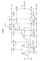
- Fig.3 is a circuit diagram of an output stage of a power amplifier provided with a circuit (shock noise reduction circuit) according to an embodiment of the present invention.
- the circuit may be provided as a semiconductor integrated device.
- the circuit may be employed as, for example, the power amplifier 12 or 14. Here, the circuit is described to be used with power amplifier 12.
- audio signals are input between terminals 60a and 60b by differential input.
- the terminals 60a, 60b are connected to the gates of p channel FETs M41 and M42, respectively.
- the FETs M41, M42 form a differential circuit together with n channel FETs M43, M44, p channel FETs M45, M48, and a switch 62.
- the disconnection timing signal output from the terminal 51 shown in Fig.1 is supplied from a terminal 63 to the switch 62.
- the switch 62 is turned ON when the disconnection timing signal is a low level, and is turned OFF when the disconnection timing signal is a high level.
- the source of FET M45 is connected to electric source Vcc, and the gate of FET M45 is connected to a terminal 66 from which a bias signal is supplied.
- a gate and a drain of FET M48 are connected to a gate of FET M46, thereby forming a current mirror circuit.
- a drain of FET M46 is connected to a drain of n channel FET M47, and the gate of FET M47 is connected to the drain of FET M41.
- the gates of p channel FETs M51 and M52 are connected to terminals 60a, 60b, respectively.
- the FETs M51 and M52 form a differential circuit together with n channel FETs M53, M54, p channel FETs M55, M58, and a switch 64.
- the disconnection timing signal output from the terminal 51 shown in Fig.1 is supplied from a terminal 65 to the switch 64.
- the switch 64 is turned ON when the disconnection timing signal is a low level, and is turned OFF when the disconnection timing signal is a high level.
- the source of FET M55 is connected to electric source Vcc, and the gate of FET M55 is connected to the terminal 66 from which a bias signal is supplied.
- the gate of FET M58 is connected to the gate and drain of FET M56 and to the gate of p channel FET M60 used for output, and the sources of FETs M56, M58, and M60 are connected to the power source Vcc, thereby forming a current mirror circuit.
- the drain of FET M56 is connected to the drain of n channel FET M57, and the gate of FET M57 is connected to the drain of FET M52.
- the gate of FET M47 is connected to the gate and drain of n channel FET M61 and the gate of n channel FET M62 used for output, and the sources of FETs M47, M61, and M62 are grounded, thereby forming a current mirror circuit.
- the FETs M60, M62 used for output have a common drain to which an output terminal 70 is connected, to thereby form a single end push-pull structure. Accordingly, audio signals are output from the output terminal 70.
- the disconnection timing signal becomes a high level to thereby turn the switches 62, 64 to an OFF state. Subsequently, the positive feed back is disconnected. Then, the bias current for the power amplifier 12, as shown in Fig.2E, gradually decreases, and eventually, the operation of the differential circuits formed by the FETs M41, M42 and FETs M51, M52, respectively, cease. Accordingly, the electric potential of the output terminal 70 gradually becomes an electric potential of the electric source Vcc or earth electric potential. Therefore, generation of shock noise occurring during the switching of the power amplifier can be restrained.
- the circuit according to an embodiment of the present invention includes a circuit for a power amplifier which amplifies and outputs an audio signal by amplifying an input audio signal using first and second differential circuits, and driving a push-pull output transistor with the outputs from the first and second differential circuits.
- the circuit includes: a signal generating part generating a disconnection timing signal for disconnecting a bias current reducing an activation current of each of the first and second differential circuits based on a switch control signal, and a positive feedback loop of each of the first and second differential circuits; a switch part being disposed in the positive feedback loops each of the first and second differential circuits, and disconnecting the positive feedback loops in response to the disconnection timing signal; and a bias unit stopping the operation of the first and second differential circuits by reducing the activation currents of the first and second differential circuits, respectively, by reduction of the bias currents. Accordingly, the shock noise generated during switching of a power amplifier can be reduced.
- the signal generation unit may include an integrator integrating the switch control signal so that a waveform of the signal is inclined, a variable bias circuit decreasing the bias current according to the inclined waveform, and a comparator generating the disconnection timing signal by comparing the inclined waveform with a reference electric potential. Accordingly, the circuit of an embodiment of the present invention can be satisfactorily executed.
- the signal generation unit may further include an inverse circuit reversing the inclined waveform, a second comparator generating a switch signal connecting the positive feedback loop of the first and second differential circuits by comparing the reversed inclined waveform with another reference electric potential, wherein the variable bias circuit outputs a first bias current which decreases, and a second bias current which increases according to the inclined waveform and the reversed inclined waveform, respectively. Accordingly, the switching between two power amplifiers can be satisfactorily controlled.
- the circuit according to an embodiment of the present invention may be a semiconductor device.
Landscapes
- Engineering & Computer Science (AREA)
- Power Engineering (AREA)
- Amplifiers (AREA)
Abstract
Description
Claims (4)
- A circuit for a power amplifier which amplifies and outputs an audio signal by amplifying an input audio signal using first and second differential circuits (M41, M42, M51, M52), and driving a push-pull output transistor (M60, M62) with the outputs from the first and second differential circuits (M41, M42, M51, M52), the circuit characterized in that:a signal generating part generating a disconnection timing signal for disconnecting a bias current reducing an activation current of each of the first and second differential circuits (M41, M42, M51, M52) based on a switch control signal, and a positive feedback loop in each of the first and second differential circuits (M41, M42, M51, M52);a switch part (62, 64) being disposed in the positive feedback loops of each of the first and second differential circuits (M41, M42, M51, M52), and disconnecting the positive feedback loops in response to the disconnection timing signal; anda bias part (M45, M55) stopping the operation of the first and second differential circuits (M41, M42, M51, M52) by reducing the activation currents of the first and second differential circuits (M41, M42, M51, M52), respectively, by reduction of the bias currents.
- The circuit as claimed in claim 1, characterized in that the signal generating part has:an integrator (42) integrating the switch control signal so that a waveform of the signal is inclined;a variable bias circuit (M30-M35, R1-R3) decreasing the bias current according to the inclined waveform; anda comparator (48) generating the disconnection timing signal by comparing the inclined waveform with a reference electric potential.
- The circuit as claimed in claim 2, characterized in that the signal generating part further has:in which the variable bias circuit (M30-M35, R1-R3) outputs a first bias current which decreases, and a second bias current which increases according to the inclined waveform and the reversed inclined waveform, respectively.an inverse circuit (44) reversing the inclined waveform; anda second comparator (46), connecting to the positive feedback loops of the first and second differential circuits (M41, M42, M51, M52), generating a switch signal by comparing the reversed inclined waveform with another reference electric potential;
- The circuit as in one of claims 1-3, characterized in that the circuit is a semiconductor device.
Applications Claiming Priority (2)
| Application Number | Priority Date | Filing Date | Title |
|---|---|---|---|
| JP2003176429A JP4182819B2 (en) | 2003-06-20 | 2003-06-20 | Shock noise reduction circuit and semiconductor integrated circuit device thereof |
| JP2003176429 | 2003-06-20 |
Publications (3)
| Publication Number | Publication Date |
|---|---|
| EP1489739A2 true EP1489739A2 (en) | 2004-12-22 |
| EP1489739A3 EP1489739A3 (en) | 2005-03-23 |
| EP1489739B1 EP1489739B1 (en) | 2006-12-13 |
Family
ID=33411010
Family Applications (1)
| Application Number | Title | Priority Date | Filing Date |
|---|---|---|---|
| EP04251144A Expired - Lifetime EP1489739B1 (en) | 2003-06-20 | 2004-02-27 | Circuit and semiconductor device |
Country Status (4)
| Country | Link |
|---|---|
| US (1) | US6967530B2 (en) |
| EP (1) | EP1489739B1 (en) |
| JP (1) | JP4182819B2 (en) |
| DE (1) | DE602004003626T2 (en) |
Cited By (2)
| Publication number | Priority date | Publication date | Assignee | Title |
|---|---|---|---|---|
| CN108233878A (en) * | 2017-12-27 | 2018-06-29 | 上海艾为电子技术股份有限公司 | A kind of AB genus audio power amplifiers |
| CN108989948A (en) * | 2018-08-08 | 2018-12-11 | 福建科立讯通信有限公司 | A kind of the voice-grade channel switching realization circuit and method of digital walkie-talkie |
Families Citing this family (1)
| Publication number | Priority date | Publication date | Assignee | Title |
|---|---|---|---|---|
| CN110719548B (en) * | 2018-07-12 | 2022-04-29 | 中兴通讯股份有限公司 | Audio processing device, audio crosstalk processing method and device |
Family Cites Families (8)
| Publication number | Priority date | Publication date | Assignee | Title |
|---|---|---|---|---|
| US4383223A (en) * | 1980-04-10 | 1983-05-10 | Motorola, Inc. | CMOS Operational amplifier employing push-pull output stage |
| US4471321A (en) * | 1982-12-17 | 1984-09-11 | Precision Monolithics, Inc. | Input current compensation circuit for superbeta transistor amplifier |
| US4516082A (en) * | 1984-02-23 | 1985-05-07 | Motorola, Inc. | Amplifier circuit for minimizing output voltage power-up transients |
| IT1185935B (en) * | 1985-09-18 | 1987-11-18 | Sgs Microelettronica Spa | LARGE VOLTAGE EXCURSION CMOS OUTPUT STAGE AND WITH LEFT CURRENT STABILIZATION |
| US4881045A (en) * | 1988-10-18 | 1989-11-14 | Hewlett-Packard Company | Transistor amplifier for high slew rates and capacitive loads |
| US5471171A (en) * | 1990-10-09 | 1995-11-28 | Kabushiki Kaisha Toshiba | Amplifier device capable of realizing high slew rate with low power consumption |
| US5656947A (en) * | 1996-07-16 | 1997-08-12 | National Semiconductor Corporation | Low noise digital output buffer |
| US6304109B1 (en) * | 2000-12-05 | 2001-10-16 | Analog Devices, Inc. | High gain CMOS amplifier |
-
2003
- 2003-06-20 JP JP2003176429A patent/JP4182819B2/en not_active Expired - Fee Related
-
2004
- 2004-02-27 US US10/789,468 patent/US6967530B2/en not_active Expired - Fee Related
- 2004-02-27 DE DE602004003626T patent/DE602004003626T2/en not_active Expired - Lifetime
- 2004-02-27 EP EP04251144A patent/EP1489739B1/en not_active Expired - Lifetime
Cited By (4)
| Publication number | Priority date | Publication date | Assignee | Title |
|---|---|---|---|---|
| CN108233878A (en) * | 2017-12-27 | 2018-06-29 | 上海艾为电子技术股份有限公司 | A kind of AB genus audio power amplifiers |
| CN108233878B (en) * | 2017-12-27 | 2021-12-10 | 上海艾为电子技术股份有限公司 | AB class audio power amplifier |
| CN108989948A (en) * | 2018-08-08 | 2018-12-11 | 福建科立讯通信有限公司 | A kind of the voice-grade channel switching realization circuit and method of digital walkie-talkie |
| CN108989948B (en) * | 2018-08-08 | 2024-03-08 | 福建科立讯通信有限公司 | Audio channel switching realization circuit and method for digital interphone |
Also Published As
| Publication number | Publication date |
|---|---|
| US20040257154A1 (en) | 2004-12-23 |
| JP2005012634A (en) | 2005-01-13 |
| DE602004003626D1 (en) | 2007-01-25 |
| DE602004003626T2 (en) | 2007-09-27 |
| EP1489739A3 (en) | 2005-03-23 |
| EP1489739B1 (en) | 2006-12-13 |
| JP4182819B2 (en) | 2008-11-19 |
| US6967530B2 (en) | 2005-11-22 |
Similar Documents
| Publication | Publication Date | Title |
|---|---|---|
| EP0792013B1 (en) | Operational amplification circuit | |
| KR20100078400A (en) | High speed differential level shifter and the boot strap driver including the same | |
| US6731169B2 (en) | Differential amplifier circuit | |
| KR100455385B1 (en) | Class AB amplifier with controlling quiescent current | |
| US7629834B2 (en) | Limiter circuit | |
| US7274254B2 (en) | Device and method for enhancing output current driving | |
| US20060170461A1 (en) | Comparator circuit having reduced pulse width distortion | |
| TW201145743A (en) | Short circuit and power limit protection circuits | |
| EP1285492A1 (en) | High impedance bias device | |
| US7830207B2 (en) | Amplifier circuit | |
| EP1489739B1 (en) | Circuit and semiconductor device | |
| US6356121B1 (en) | Very low-power comparison device | |
| US7525359B2 (en) | Duty cycle correction amplification circuit | |
| US5481213A (en) | Cross-conduction prevention circuit for power amplifier output stage | |
| US20050156666A1 (en) | Low-voltage differential amplifier | |
| US20070024367A1 (en) | Operational amplifier and constant-current generation circuit using the same | |
| US7161431B2 (en) | Class B amplifier with process variation independent deadband | |
| CN103001594B (en) | Amplifying circuit | |
| US6570450B2 (en) | Efficient AC coupled CMOS RF amplifier | |
| EP0685125B1 (en) | Cross-conduction prevention circuit for power amplifier output stage | |
| US6583670B2 (en) | CMOS current amplifier | |
| JP4672883B2 (en) | Semiconductor device | |
| KR100668455B1 (en) | Variable gain amplifier | |
| US4956613A (en) | Differential amplifier having externally controllable power consumption | |
| US6859100B2 (en) | Class-A amplifier circuit having output voltage varied according to input voltage |
Legal Events
| Date | Code | Title | Description |
|---|---|---|---|
| PUAI | Public reference made under article 153(3) epc to a published international application that has entered the european phase |
Free format text: ORIGINAL CODE: 0009012 |
|
| AK | Designated contracting states |
Kind code of ref document: A2 Designated state(s): AT BE BG CH CY CZ DE DK EE ES FI FR GB GR HU IE IT LI LU MC NL PT RO SE SI SK TR |
|
| AX | Request for extension of the european patent |
Extension state: AL HR LT LV MK |
|
| PUAL | Search report despatched |
Free format text: ORIGINAL CODE: 0009013 |
|
| RIN1 | Information on inventor provided before grant (corrected) |
Inventor name: YAMANAKA, YUJI,MITSUMI ELECTRIC CO., LTD. Inventor name: OMATA, JUN-ICHI,MITSUMI ELECTRIC CO., LTD. Inventor name: ODA, TOMOMI,MITSUMI ELECTRIC CO., LTD. |
|
| AK | Designated contracting states |
Kind code of ref document: A3 Designated state(s): AT BE BG CH CY CZ DE DK EE ES FI FR GB GR HU IE IT LI LU MC NL PT RO SE SI SK TR |
|
| AX | Request for extension of the european patent |
Extension state: AL HR LT LV MK |
|
| 17P | Request for examination filed |
Effective date: 20050502 |
|
| AKX | Designation fees paid |
Designated state(s): DE GB |
|
| GRAP | Despatch of communication of intention to grant a patent |
Free format text: ORIGINAL CODE: EPIDOSNIGR1 |
|
| GRAS | Grant fee paid |
Free format text: ORIGINAL CODE: EPIDOSNIGR3 |
|
| GRAA | (expected) grant |
Free format text: ORIGINAL CODE: 0009210 |
|
| AK | Designated contracting states |
Kind code of ref document: B1 Designated state(s): DE GB |
|
| REG | Reference to a national code |
Ref country code: GB Ref legal event code: FG4D |
|
| REF | Corresponds to: |
Ref document number: 602004003626 Country of ref document: DE Date of ref document: 20070125 Kind code of ref document: P |
|
| PLBE | No opposition filed within time limit |
Free format text: ORIGINAL CODE: 0009261 |
|
| STAA | Information on the status of an ep patent application or granted ep patent |
Free format text: STATUS: NO OPPOSITION FILED WITHIN TIME LIMIT |
|
| 26N | No opposition filed |
Effective date: 20070914 |
|
| PGFP | Annual fee paid to national office [announced via postgrant information from national office to epo] |
Ref country code: DE Payment date: 20190212 Year of fee payment: 16 Ref country code: GB Payment date: 20190227 Year of fee payment: 16 |
|
| REG | Reference to a national code |
Ref country code: DE Ref legal event code: R119 Ref document number: 602004003626 Country of ref document: DE |
|
| GBPC | Gb: european patent ceased through non-payment of renewal fee |
Effective date: 20200227 |
|
| PG25 | Lapsed in a contracting state [announced via postgrant information from national office to epo] |
Ref country code: DE Free format text: LAPSE BECAUSE OF NON-PAYMENT OF DUE FEES Effective date: 20200901 Ref country code: GB Free format text: LAPSE BECAUSE OF NON-PAYMENT OF DUE FEES Effective date: 20200227 |