EP1489436A1 - Radiation detecting cassette - Google Patents
Radiation detecting cassette Download PDFInfo
- Publication number
- EP1489436A1 EP1489436A1 EP04013465A EP04013465A EP1489436A1 EP 1489436 A1 EP1489436 A1 EP 1489436A1 EP 04013465 A EP04013465 A EP 04013465A EP 04013465 A EP04013465 A EP 04013465A EP 1489436 A1 EP1489436 A1 EP 1489436A1
- Authority
- EP
- European Patent Office
- Prior art keywords
- solid
- state radiation
- radiation detector
- radiation
- inner frame
- Prior art date
- Legal status (The legal status is an assumption and is not a legal conclusion. Google has not performed a legal analysis and makes no representation as to the accuracy of the status listed.)
- Granted
Links
- 230000005855 radiation Effects 0.000 title claims abstract description 109
- 239000011359 shock absorbing material Substances 0.000 claims abstract description 11
- 238000001454 recorded image Methods 0.000 claims description 2
- 230000035939 shock Effects 0.000 abstract description 18
- 230000008878 coupling Effects 0.000 abstract description 15
- 238000010168 coupling process Methods 0.000 abstract description 15
- 238000005859 coupling reaction Methods 0.000 abstract description 15
- 239000000463 material Substances 0.000 description 14
- 238000006243 chemical reaction Methods 0.000 description 8
- 229920005989 resin Polymers 0.000 description 5
- 239000011347 resin Substances 0.000 description 5
- 238000010276 construction Methods 0.000 description 4
- 239000006260 foam Substances 0.000 description 4
- 238000000034 method Methods 0.000 description 4
- 230000035945 sensitivity Effects 0.000 description 4
- JOYRKODLDBILNP-UHFFFAOYSA-N Ethyl urethane Chemical compound CCOC(N)=O JOYRKODLDBILNP-UHFFFAOYSA-N 0.000 description 2
- 239000004020 conductor Substances 0.000 description 2
- 230000000694 effects Effects 0.000 description 2
- 229910052751 metal Inorganic materials 0.000 description 2
- 239000002184 metal Substances 0.000 description 2
- 230000002093 peripheral effect Effects 0.000 description 2
- 239000003190 viscoelastic substance Substances 0.000 description 2
- 229910000838 Al alloy Inorganic materials 0.000 description 1
- 229920002799 BoPET Polymers 0.000 description 1
- 229920001875 Ebonite Polymers 0.000 description 1
- 229910000861 Mg alloy Inorganic materials 0.000 description 1
- 229930182556 Polyacetal Natural products 0.000 description 1
- 239000004743 Polypropylene Substances 0.000 description 1
- XAGFODPZIPBFFR-UHFFFAOYSA-N aluminium Chemical compound [Al] XAGFODPZIPBFFR-UHFFFAOYSA-N 0.000 description 1
- 238000001514 detection method Methods 0.000 description 1
- 238000003745 diagnosis Methods 0.000 description 1
- 239000010408 film Substances 0.000 description 1
- NBVXSUQYWXRMNV-UHFFFAOYSA-N fluoromethane Chemical compound FC NBVXSUQYWXRMNV-UHFFFAOYSA-N 0.000 description 1
- 239000011521 glass Substances 0.000 description 1
- 239000011810 insulating material Substances 0.000 description 1
- 230000001678 irradiating effect Effects 0.000 description 1
- RQQRAHKHDFPBMC-UHFFFAOYSA-L lead(ii) iodide Chemical compound I[Pb]I RQQRAHKHDFPBMC-UHFFFAOYSA-L 0.000 description 1
- 239000007769 metal material Substances 0.000 description 1
- 125000004123 n-propyl group Chemical group [H]C([H])([H])C([H])([H])C([H])([H])* 0.000 description 1
- 230000000149 penetrating effect Effects 0.000 description 1
- 239000004033 plastic Substances 0.000 description 1
- 238000007747 plating Methods 0.000 description 1
- 229920000515 polycarbonate Polymers 0.000 description 1
- 239000004417 polycarbonate Substances 0.000 description 1
- 229920006267 polyester film Polymers 0.000 description 1
- 229920000139 polyethylene terephthalate Polymers 0.000 description 1
- 229920006324 polyoxymethylene Polymers 0.000 description 1
- -1 polypropylene Polymers 0.000 description 1
- 229920001155 polypropylene Polymers 0.000 description 1
- 238000002601 radiography Methods 0.000 description 1
- 239000004065 semiconductor Substances 0.000 description 1
- 239000007787 solid Substances 0.000 description 1
- 125000006850 spacer group Chemical group 0.000 description 1
- 239000000758 substrate Substances 0.000 description 1
- 239000010409 thin film Substances 0.000 description 1
Images

Classifications
-
- G—PHYSICS
- G01—MEASURING; TESTING
- G01T—MEASUREMENT OF NUCLEAR OR X-RADIATION
- G01T1/00—Measuring X-radiation, gamma radiation, corpuscular radiation, or cosmic radiation
- G01T1/16—Measuring radiation intensity
- G01T1/24—Measuring radiation intensity with semiconductor detectors
- G01T1/244—Auxiliary details, e.g. casings, cooling, damping or insulation against damage by, e.g. heat, pressure or the like
Definitions
- This invention relates to a radiation detecting cassette having a solid state radiation detector accommodated within a casing.
- the shock absorbing material may be any of materials that include, but are not limited to, a viscoelastic material such as a soft rubber or a gel, and a foamed material such as styrene-foam or urethane foam.
- FIG. 1 is a plan view of an embodiment of a radiation detecting cassette according to the present invention, with an upper shell half removed
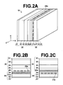
- FIG. 2A is a perspective view of a solid-state radiation detector used for the radiation detecting cassette in FIG. 1
- FIG. 2B is a cross sectional view taken through plane X-Z of FIG. 2A
- FIG. 2C is a cross sectional view taken through plane X-Y of FIG. 2A
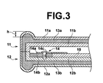
- FIG. 3 is a cross sectional view of the radiation detecting cassette including the upper shell half, taken along line III-III of FIG. 1.
- the reading light photoconductive layer 24 is made of a material which is high in sensitivity to an electromagnetic wave in the region from near-ultraviolet to blue (300 to 550 nm) and low in sensitivity to an electromagnetic wave in the red region (not shorter than 700 nm)
- the planar light source section 30 (EL emitter) is required to be made of a material which emits light having an electromagnetic wave in the region from near-ultraviolet to blue (550 nm or less).
Landscapes
- Physics & Mathematics (AREA)
- Health & Medical Sciences (AREA)
- Life Sciences & Earth Sciences (AREA)
- General Physics & Mathematics (AREA)
- High Energy & Nuclear Physics (AREA)
- Molecular Biology (AREA)
- Spectroscopy & Molecular Physics (AREA)
- Measurement Of Radiation (AREA)
- Radiography Using Non-Light Waves (AREA)
- Apparatus For Radiation Diagnosis (AREA)
Abstract
Description
- This invention relates to a radiation detecting cassette having a solid state radiation detector accommodated within a casing.
- In the field of radiography for medical diagnosis and the like, various solid-state radiation detectors (whose main part comprises semiconductors; hereinafter also simply referred to as "detectors") which detect radiation penetrating a subject and produce an image signal carrying radiographic image information of the subject (see, for example, U.S. patent No. 6,268,614 and Japanese Unexamined Patent Publication No. 2000-284056 have recently been proposed and brought into practical use. Concomitantly with this, various radiation detecting cassettes having a case accommodating therein such a solid-state radiation detector and the like (see, for example, U.S. Patent Laid-Open No. 20020014594 and Japanese Unexamined Patent Publication No. 2002-014170 have been proposed.
- Such a radiation detecting cassette is relatively thin and made in portable size. This allows radiophotographing with a very high degree of freedom. For example, even for a patient who is not ambulatory, a radiophotograph can be taken by placing the radiation detecting cassette under a body part of the patient to be radiophotographed while keeping the patient on a bed, and then moving a radiation source of a radiation image information recording apparatus to a position on a side of the patient opposite the radiation detecting cassette.
- As one specific example, the radiation detecting cassette may have a construction where the solid-state radiation detector and an electric circuit board for processing a signal detected by the detector are secured inside a casing of the cassette, and where the solid-state radiation detector and the electric circuit board are connected with each other via a flexible circuit board.
- In order to prevent damage to the solid-state radiation detector accommodated within such a radiation detecting cassette when the cassette is subjected to outside impact, aforementioned Japanese Unexamined Patent Publication No. 2002-014170 proposes a radiation detecting cassette, in which a shock absorbing material is disposed on an upper side (i.e., a side to be exposed to the radiation) of the solid-state radiation detector, while a lower side of the solid-state radiation detector is secured to the frame. With this configuration, the solid-state radiation detector cannot move towards the bottom of the radiation detecting cassette. Therefore, if the solid-state radiation detector is subjected to a shock in the direction towards the bottom thereof, shock cannot be absorbed.
- On the other hand, when elastomeric bodies such as rubber or gel are used to sandwich the solid-state radiation detector therebetween for supporting the upper and lower surfaces of the detector as proposed in U.S. Patent Laid-Open No. 20020014594 mentioned above, it is difficult to ensure the positional precision of the solid-state radiation detector within the casing because the elastic bodies tend to change their shape.
- The present invention was developed in view of the foregoing problems, and has an object to provide a radiation detecting cassette which improves positional precision of the solid-state radiation detector within the casing, while ensuring the shock resistance properties of the radiation detecting cassette.
- In accordance with the present invention, there is provided a radiation detecting cassette comprising: a plate-type solid-state radiation detector for recording image information carried by radiation upon exposure to the radiation and outputting an image signal representing the recorded image information; and a casing for accommodating therein the solid-state radiation detector, wherein the casing is constituted by an outer frame and an inner frame, wherein a limiting member for limiting movement of the inner frame relative to the outer frame is provided between the inner side surface of the outer frame and the outer side surface of the inner frame, and wherein a space between the outer frame and the inner frame is filled with a shock absorbing material.
- As used herein, the term "solid-state radiation detector" means a detector, which detects radiation, carrying image information of an object, and outputs an image signal representing a radiation image of the object. The solid-state radiation detector converts the incident radiation into electric charges directly or after converting the radiation into light, accumulates the electric charges at charge accumulating sections, and thereafter outputs the electric charges to the exterior. In this manner, the image signal representing the radiation image of the object can be obtained.
- There are various types of solid-state radiation detectors. For example, from the aspect of a charge forming process for converting the radiation into electric charges, the solid-state radiation detectors may be classified into photo conversion type solid-state radiation detectors and direct conversion type solid-state radiation detectors. With the photo conversion type solid-state radiation detectors, the fluorescence, which is produced by a fluorescent material when it is exposed to radiation carrying image information, is detected by a photoelectric conversion device, and the thus obtained electric charges are accumulated at a charge accumulating sections of the photoelectric conversion devices. The accumulated electric charges are then converted into an image signal (i.e., an electric signal), and the image signal is fed out. With the direct conversion type solid-state radiation detectors, electric charges, which are generated in a radiation conductive material when it is exposed to radiation carrying image information, are collected by charge collecting electrodes and accumulated at charge accumulating sections. The accumulated charges are then converted into an electric signal, and the electric signal is fed out. On the other hand, from the aspect of a charge reading process for reading the accumulated electric charges to the exterior, the solid-state radiation detectors may be classified into, for example, thin-film transistor (TFT) reading type solid-state radiation detectors, wherein TFT's, each of which is connected to one of the charge accumulating sections, are operated successively in order to read the accumulated electric charges; photo reading type solid-state radiation detectors, wherein the accumulated electric charges are read by irradiating reading light (an electromagnetic wave for reading) to the solid-state radiation detectors; and improved direct conversion type solid-state radiation detectors, which utilize a combination of the direct conversion type techniques and the photo reading type techniques proposed in U.S. Patent No. 6,268,614 and Japanese Unexamined Patent Publication No. 2000-284056 mentioned above. The radiation detecting cassette in accordance with the present invention may comprise any type of solid-state radiation detector housed within a case.
- The shock absorbing material may be any of materials that include, but are not limited to, a viscoelastic material such as a soft rubber or a gel, and a foamed material such as styrene-foam or urethane foam.
- In the radiation detecting cassette of the present invention, the outer frame is preferably flexible.
- In the radiation detecting cassette according to the present invention, a casing for accommodating therein a solid-state radiation detector may comprise: an outer frame; an inner frame; and a limiting member which is disposed between the inner side surface of the outer frame and the outer side surface of the inner frame, and serves to limit the movement of the inner frame relative to the outer frame, and a space between the outer frame and the inner frame is filled with a shock absorbing material in order to impart shock absorbency to the casing itself. This enables to provide a sufficient shock resistance without holding the solid-state radiation detector between elastic bodies, thereby improving positional precision of the solid-state radiation detector within the casing thereof while ensuring the shock resistance properties.
- Further, according to the present invention, the outer frame may be made to be flexible such that the outer frame can be readily deformed, whereby the shock applied thereto is more effectively absorbed.
-
- FIG. 1 is a plan view of an embodiment of a radiation detecting cassette according to the present invention, shown with an upper shell half removed;
- FIG. 2A is a perspective view of a solid-state radiation detector used for the radiation detecting cassette in FIG. 1, FIG. 2B is a cross sectional view taken through plane X-Z of FIG. 2A, and FIG. 2C is a cross sectional view taken through plane X-Y of FIG. 2A; and
- FIG. 3 is a cross sectional view of the radiation detecting cassette including the upper shell half, taken along line III-III of FIG. 1.
-
- An embodiment of the radiation detecting cassette in accordance with the present invention will be described hereinbelow. FIG. 1 is a plan view of an embodiment of a radiation detecting cassette according to the present invention, with an upper shell half removed, FIG. 2A is a perspective view of a solid-state radiation detector used for the radiation detecting cassette in FIG. 1, FIG. 2B is a cross sectional view taken through plane X-Z of FIG. 2A, FIG. 2C is a cross sectional view taken through plane X-Y of FIG. 2A, and FIG. 3 is a cross sectional view of the radiation detecting cassette including the upper shell half, taken along line III-III of FIG. 1.
- A
radiation detecting cassette 1 has a casing constituted by upper andlower shell halves radiation detecting cassette 1 includes a solid-state radiation detector 10, which is an image pickup device; an electric circuit board (not shown) for providing an image signal by detecting a current from the solid-state radiation detector 10; a flexible circuit board (not shown) for connecting the solid-state radiation detector 10 and the electric circuit board; and a power supply unit (not shown), all of which are housed in the casing. - The
upper shell half 11 comprises: a generally parallelepiped-shapedouter frame 11a having one open side; a generally parallelepiped-shapedinner frame 11b having one open side; and a coupling member 11c disposed between the inner side surface of theouter frame 11a and the outer side surface of theinner frame 11b. The coupling member 11c is secured at both ends to the inner side surface of theouter frame 11a and the outer side surface of theinner frame 11b. A space extending between theouter frame 11a and theinner frame 11b is filled with ashock absorbing material 13a. - Similarly, the
lower shell half 12 comprises: a generally parallelepiped-shapedouter frame 12a having one open side; a generally parallelepiped-shapedinner frame 12b having one open side; and acoupling member 12c disposed between the inner side surface of theouter frame 12a and the outer side surface of theinner frame 12b. Thecoupling member 12c is secured at both ends to the inner side surface of theouter frame 12a and the outer side surface of theinner frame 12b. A space extending between theouter frame 12a and theinner frame 12b is filled with ashock absorbing material 13b. - Both of the
inner frames lower shell halves - The wider the space between the
outer frames inner frames radiation detecting cassette 1 accordingly becomes larger. Thus, the aforementioned space is preferably about 5 mm. - Since the
coupling members 11c and 12c also serve as a limiting member to limit the respective movements of theinner frames outer frames coupling members 11c and 12c have a certain degree of rigidity. However, having an excessive degree of rigidity larger than necessary is undesirable in terms of shock absorbency. Thus, thecoupling members 11c and 12c are preferably formed of a material which has a higher rigidity than that of theshock absorbing material - Since portions, on which the
coupling members 11c and 12c are provided, are inferior in shock absorbency to the remaining area, it is desirable that thecoupling members 11c and 12c are not provided near any of the corners of the casing which are apt to be subjected to an impact. Specifically, it is desirable that thecoupling members 11c, 12c are not provided in the range extending within 10% of the length of each of the sides from each corner included thereby, and preferably not within 20% of the length of each side from each corner included thereby. - In the specific embodiment described above, the
coupling members 11c, 12c are fixedly attached at both ends. However, the radiation detecting cassette of the present invention is not limited to this construction. Both ends or one end of thecoupling member 11c, 12c may not be fixedly attached so long as thecoupling member 11c, 12c serves as a limiting member for limiting the movement of the inner frame relative to the outer frame. - The
shock absorbing material - The
outer frames outer frames 11a and/or 12a. When an internal pressure produced by filling theshock absorbing material outer frames outer frames - Further, the peripheral edge of the main surface of each of the
outer frames - The solid-
state radiation detector 10 has a layered structure formed by placing in mutually superposed relationship a solid-stateradiation detecting section 20 and a planarlight source section 30 on a glass substrate (not shown). - The solid-state
radiation detecting section 20 serves to record radiation image information as a latent image, and to generate an electric current corresponding to the latent image as the electrostatic latent image is scanned by a reading electromagnetic wave (hereinafter referred to as reading light). The solid-stateradiation detecting section 20 is constituted by: a first electricallyconductive layer 21 which is permeable to recording radiation such as X-ray passing through an object (hereinafter referred to as recording light); a recordinglight photoconductive layer 22 which generates a charge upon exposure to the recording light and exhibits electric conductivity; acharge transfer layer 23 which behaves like a substantially insulating material to a charge of the latent image polarity (a negative charge) accumulated in the firstconductive layer 21 and behaves substantially as a conductive material to a charge of the transfer polarity (a positive charge, in this example) opposite to that of the latent image polarity; a reading lightphotoconductive layer 24 which generates an electric current upon exposure to the reading light and exhibits conductivity; and a second electricallyconductive layer 25 permeable to the reading light. They are superimposed in this order. A charge accumulating section is formed at the interface between the recording lightphotoconductive layer 22 and thecharge transfer layer 23. - The first electrically
conductive layer 21 and second electricallyconductive layer 25 serve as electrodes, respectively. The electrode constituted by the firstconductive layer 21 is a two-dimensional flat plate electrode, while the electrode constituted by the second electricallyconductive layer 25 is a stripe electrode constructed of a large number of electrode elements (line electrode elements) 25a disposed at intervals of a pixel pitch (for example, an electrostatically recording medium disclosed in Japanese Unexamined Patent Publication No. 2000-105297). The direction in which theelements 25a are arranged is the main scanning direction, and the longitudinal direction of theelements 25a is the subscanning direction. Eachelement 25a is connected to a current detecting device on the electric circuit board via the flexible circuit board. - Preferably, the reading light
photoconductive layer 24 is made of a material which is high in sensitivity to an electromagnetic wave in the region from near-ultraviolet to blue (300 to 550 nm) and low in sensitivity to an electromagnetic wave in the red region (not shorter than 700 nm), e.g., a photoconductive material containing as a major component at least one of a-Se, PbI2, Bi12 (Ge, Si) O20, perylenebisimide (R=n-propyl) and perylenebisimide (R=n-neopentyl). In the present embodiment, a-Se is used. - The planar
light source section 30 is an EL (electroluminescent) light emitter and is constituted by an electricallyconductive layer 31, anEL layer 32, and an electricallyconductive layer 33. An insulatinglayer 34 is disposed between the second electricallyconductive layer 25 of the solid-stateradiation detecting section 20 and the electricallyconductive layer 33. The electricallyconductive layer 31 is a stripe electrode having a large number of electrode elements (line electrode elements) 31a disposed at intervals of a pixel pitch such that eachelectrode element 31a extends transversely of (in this embodiment, substantially perpendicular to) theelements 25a of the solid-stateradiation detecting section 20. Thus, a large number of linear light sources, which are respectively constituted byelectrode elements 31a (the hatched region in the drawing), are arrayed in a planar state. Each of theelements 31a is connected to a light source controlling device on the electric circuit board via the flexible circuit board. Therespective elements 31a are made of a material that transmits the EL light from theEL layer 32. The electricallyconductive layer 33 is a plate electrode made of a material by which the EL light from theEL layer 32 is completely reflected. - The light source controlling device individually or simultaneously applies a predetermined voltage between each of the
elements 31a and a corresponding portion facing thereto of the electricallyconductive layer 33. More particularly, the light source controlling device sequentially applies a predetermined DC voltage between therespective elements 31a and the electricallyconductive layer 33. As the DC voltage is applied, EL light is emitted from a portion of theEL layer 32 positioned between therelevant element 31a and the electricallyconductive layer 33. Since theelement 31a is linear in shape, the EL light transmitted through theelement 31a is utilized as linear reading light. Thus, the planarlight source section 30 becomes equivalent to those constructed of a large number of minute linear light sources arranged in a plane. EL-emission is produced by sequentially selecting a predetermined number of theelements 31a, so that the solid-stateradiation detecting section 20 is electrically scanned by the reading light. - As mentioned above, since the reading light
photoconductive layer 24 is made of a material which is high in sensitivity to an electromagnetic wave in the region from near-ultraviolet to blue (300 to 550 nm) and low in sensitivity to an electromagnetic wave in the red region (not shorter than 700 nm), the planar light source section 30 (EL emitter) is required to be made of a material which emits light having an electromagnetic wave in the region from near-ultraviolet to blue (550 nm or less). - The solid-
state radiation detector 10 is supported byholders 14 which are fixed to theinner frame 12b of thelower shell half 12. - The
holder 14 comprises: aspacer 14b, which is substantially as high as the solid-state radiation detector 10 and includes at the center thereof an aperture that is substantially as large as solid-state radiation detector 10; a holdingmember 14a disposed on the upper surface side of the solid-state radiation detector 10, and ascrew 14c by which theholder 14 is fixedly attached to theinner frame 12b. Thespace 14b and the holdingmember 14a are stacked on the inner frame in this order. - This arrangement imparts shock absorbency to the casing that accommodates therein the solid-
state radiation detector 10. Consequently, it is allowed to rigidly secure the solid-state radiation detector 10 toinner frame 12b of the casing, as a result of which, the positional precision of the solid-state radiation detector 10 within the casing is enhanced, and deflection of the solid-state radiation detector 10 due to the self-weight thereof and distortion of the component are prevented. - In the specific embodiment described above, the casing has a double-walled construction comprising the outer frame and the inner frame. However, the radiation detecting cassette of the present invention is not limited thereto, and only the entire peripheral edge or the corners may have a double-walled construction.
Claims (2)
- A radiation detecting cassette comprising:wherein the casing is constituted by an outer frame and an inner frame,a plate-type solid-state radiation detector for recording image information carried by radiation upon exposure to the radiation and supplying an image signal representing the recorded image information; anda casing for accommodating therein the solid-state radiation detector,
wherein a limiting member for limiting movement of the inner frame relative to the outer frame is provided between the inner side surface of the outer frame and the outer side surface of the inner frame, and
wherein a space between the outer frame and the inner frame is filled with a shock absorbing material. - A radiation detecting cassette according to claim 1, wherein the outer frame is flexible.
Applications Claiming Priority (2)
| Application Number | Priority Date | Filing Date | Title |
|---|---|---|---|
| JP2003163300A JP4248940B2 (en) | 2003-06-09 | 2003-06-09 | Radiation detection cassette |
| JP2003163300 | 2003-06-09 |
Publications (2)
| Publication Number | Publication Date |
|---|---|
| EP1489436A1 true EP1489436A1 (en) | 2004-12-22 |
| EP1489436B1 EP1489436B1 (en) | 2010-03-24 |
Family
ID=33410877
Family Applications (1)
| Application Number | Title | Priority Date | Filing Date |
|---|---|---|---|
| EP04013465A Expired - Lifetime EP1489436B1 (en) | 2003-06-09 | 2004-06-08 | Radiation detecting cassette |
Country Status (4)
| Country | Link |
|---|---|
| US (1) | US7183556B2 (en) |
| EP (1) | EP1489436B1 (en) |
| JP (1) | JP4248940B2 (en) |
| DE (1) | DE602004026137D1 (en) |
Cited By (4)
| Publication number | Priority date | Publication date | Assignee | Title |
|---|---|---|---|---|
| WO2007139638A3 (en) * | 2006-05-26 | 2008-04-24 | Carestream Health Inc | Encasement for digital radiography detector |
| EP1853970B1 (en) * | 2005-02-10 | 2012-04-11 | Koninklijke Philips Electronics N.V. | Portable x-ray detector plate with shock absorption |
| EP1923723A3 (en) * | 2006-11-20 | 2012-08-29 | Konica Minolta Medical & Graphic, Inc. | Cassette type radiation image detector |
| EP2051109A3 (en) * | 2007-09-12 | 2013-06-05 | Carestream Health, Inc. | Assembly features and shock protection for a digital radiography detector |
Families Citing this family (29)
| Publication number | Priority date | Publication date | Assignee | Title |
|---|---|---|---|---|
| JP4384091B2 (en) * | 2005-07-13 | 2009-12-16 | キヤノン株式会社 | Portable radiography system |
| US7798476B2 (en) * | 2006-01-03 | 2010-09-21 | General Electric Company | Shock absorber for medical imaging device |
| JP4921180B2 (en) | 2006-01-25 | 2012-04-25 | キヤノン株式会社 | Radiation detection apparatus and radiation imaging system |
| US7396159B2 (en) * | 2006-06-07 | 2008-07-08 | General Electric Company | X-ray detector panel methods and apparatus |
| US7488946B2 (en) * | 2006-10-03 | 2009-02-10 | General Electric Company | Digital x-ray detectors |
| US20080078940A1 (en) * | 2006-10-03 | 2008-04-03 | General Electric Company | Portable imaging device having shock absorbent assembly |
| JP4879875B2 (en) * | 2007-09-21 | 2012-02-22 | 富士フイルム株式会社 | Radiation detector |
| JP4796030B2 (en) * | 2007-09-27 | 2011-10-19 | 富士フイルム株式会社 | Image detector and image capturing system |
| JP5069992B2 (en) * | 2007-09-27 | 2012-11-07 | 富士フイルム株式会社 | Image detector and image capturing system |
| JP4940125B2 (en) * | 2007-12-28 | 2012-05-30 | 富士フイルム株式会社 | Radiation detector |
| CN101507611B (en) * | 2008-02-13 | 2014-06-25 | Ge医疗系统环球技术有限公司 | Detector panel and X-ray imaging device |
| CN101507610B (en) * | 2008-02-13 | 2012-12-12 | Ge医疗系统环球技术有限公司 | Detector panel and X-ray imaging device |
| JP4847492B2 (en) | 2008-06-02 | 2011-12-28 | キヤノン株式会社 | Radiation detection apparatus, radiation detection system, and control method thereof |
| US7800065B2 (en) * | 2008-07-02 | 2010-09-21 | General Electric Company | Methods and apparatus for conducting heat from an electronic assembly while providing shock protection |
| JP2010071726A (en) * | 2008-09-17 | 2010-04-02 | Fujifilm Corp | Radiation detecting device and system of photographing radiation image |
| JP5137763B2 (en) | 2008-09-26 | 2013-02-06 | 富士フイルム株式会社 | Radiation detection apparatus and radiographic imaging system |
| JP2011117760A (en) * | 2009-12-01 | 2011-06-16 | Toshiba Corp | Planar x-ray detector |
| US8766200B2 (en) | 2012-01-03 | 2014-07-01 | General Electric Company | Mechanical shock isolation for a radiographic device |
| JP2013217769A (en) * | 2012-04-09 | 2013-10-24 | Canon Inc | Radiation detection apparatus |
| JP5627049B2 (en) * | 2013-06-07 | 2014-11-19 | 富士フイルム株式会社 | Electronic cassette |
| JP6700667B2 (en) * | 2014-06-18 | 2020-05-27 | キヤノン株式会社 | Radiation imaging apparatus and radiation imaging system |
| JP6633864B2 (en) | 2015-08-07 | 2020-01-22 | キヤノン株式会社 | Radiation imaging apparatus and radiation imaging system |
| JP6812759B2 (en) * | 2016-11-14 | 2021-01-13 | コニカミノルタ株式会社 | Portable radiation imaging device |
| US10506994B2 (en) | 2017-08-29 | 2019-12-17 | General Electric Company | Apparatus for a radiographic device |
| US10045748B1 (en) | 2017-09-29 | 2018-08-14 | General Electric Company | X-ray detector structure |
| JP7242281B2 (en) * | 2018-12-17 | 2023-03-20 | キヤノン株式会社 | radiography equipment |
| US20210048543A1 (en) * | 2019-08-13 | 2021-02-18 | Vieworks Co., Ltd. | X-ray detector cover and x-ray detector having same |
| JP2022121107A (en) * | 2021-02-08 | 2022-08-19 | キヤノン株式会社 | radiography equipment |
| JP7676989B2 (en) * | 2021-06-24 | 2025-05-15 | コニカミノルタ株式会社 | Radiation detector |
Citations (3)
| Publication number | Priority date | Publication date | Assignee | Title |
|---|---|---|---|---|
| EP0603709A2 (en) * | 1992-12-23 | 1994-06-29 | E.I. Du Pont De Nemours And Company | Electronic cassette for recording X-ray images |
| JP2002014170A (en) * | 2000-06-27 | 2002-01-18 | Canon Inc | X-ray image input device |
| US20020014594A1 (en) * | 2000-06-27 | 2002-02-07 | Takashi Endo | Radiation imaging system |
Family Cites Families (4)
| Publication number | Priority date | Publication date | Assignee | Title |
|---|---|---|---|---|
| EP0898421A3 (en) | 1997-08-19 | 2001-12-05 | Fuji Photo Film Co., Ltd. | Electrostatic recording member, electrostatic latent image recording apparatus, and electrostatic latent image read-out apparatus |
| JP4040201B2 (en) | 1999-03-30 | 2008-01-30 | 富士フイルム株式会社 | Radiation solid state detector, and radiation image recording / reading method and apparatus using the same |
| JP4497663B2 (en) * | 2000-06-09 | 2010-07-07 | キヤノン株式会社 | Radiation imaging equipment |
| DE102004042365A1 (en) * | 2003-09-12 | 2005-04-14 | Siemens Ag | X-ray detector e.g. CMOS chip, has detector plate with detector units accommodated in housing in floating manner using spring unit, where detector plate is attached to one of inside wall of housing and substrate |
-
2003
- 2003-06-09 JP JP2003163300A patent/JP4248940B2/en not_active Expired - Fee Related
-
2004
- 2004-06-07 US US10/861,925 patent/US7183556B2/en not_active Expired - Lifetime
- 2004-06-08 EP EP04013465A patent/EP1489436B1/en not_active Expired - Lifetime
- 2004-06-08 DE DE602004026137T patent/DE602004026137D1/en not_active Expired - Lifetime
Patent Citations (3)
| Publication number | Priority date | Publication date | Assignee | Title |
|---|---|---|---|---|
| EP0603709A2 (en) * | 1992-12-23 | 1994-06-29 | E.I. Du Pont De Nemours And Company | Electronic cassette for recording X-ray images |
| JP2002014170A (en) * | 2000-06-27 | 2002-01-18 | Canon Inc | X-ray image input device |
| US20020014594A1 (en) * | 2000-06-27 | 2002-02-07 | Takashi Endo | Radiation imaging system |
Non-Patent Citations (1)
| Title |
|---|
| PATENT ABSTRACTS OF JAPAN vol. 2002, no. 05 3 May 2002 (2002-05-03) * |
Cited By (8)
| Publication number | Priority date | Publication date | Assignee | Title |
|---|---|---|---|---|
| EP1853970B1 (en) * | 2005-02-10 | 2012-04-11 | Koninklijke Philips Electronics N.V. | Portable x-ray detector plate with shock absorption |
| WO2007139638A3 (en) * | 2006-05-26 | 2008-04-24 | Carestream Health Inc | Encasement for digital radiography detector |
| US7495226B2 (en) | 2006-05-26 | 2009-02-24 | Carestream Health, Inc. | Compact and durable encasement for a digital radiography detector |
| US7842928B2 (en) | 2006-05-26 | 2010-11-30 | Carestream Health, Inc. | Compact and durable encasement for a digital radiography detector |
| US7989773B2 (en) | 2006-05-26 | 2011-08-02 | Carestream Health, Inc. | Compact and durable encasement for a digital radiography detector |
| US8389944B2 (en) | 2006-05-26 | 2013-03-05 | Carestream Health, Inc. | Compact and durable encasement for a digital radiography detector |
| EP1923723A3 (en) * | 2006-11-20 | 2012-08-29 | Konica Minolta Medical & Graphic, Inc. | Cassette type radiation image detector |
| EP2051109A3 (en) * | 2007-09-12 | 2013-06-05 | Carestream Health, Inc. | Assembly features and shock protection for a digital radiography detector |
Also Published As
| Publication number | Publication date |
|---|---|
| US20050017188A1 (en) | 2005-01-27 |
| EP1489436B1 (en) | 2010-03-24 |
| DE602004026137D1 (en) | 2010-05-06 |
| JP4248940B2 (en) | 2009-04-02 |
| JP2004361879A (en) | 2004-12-24 |
| US7183556B2 (en) | 2007-02-27 |
Similar Documents
| Publication | Publication Date | Title |
|---|---|---|
| EP1489436B1 (en) | Radiation detecting cassette | |
| US7057181B2 (en) | Radiation detecting cassette | |
| EP1643305B1 (en) | Radiographic apparatus | |
| US5804832A (en) | Digital array for radiographic imaging | |
| JP3486515B2 (en) | Glass substrate holding structure and radiation imaging apparatus | |
| US7429737B2 (en) | Retrofit digital mammography detector | |
| US8901505B2 (en) | Cassette for radiographic imaging | |
| CN101185575B (en) | Cassette type radiation image detector | |
| JP2011059058A (en) | Radiographic imaging device | |
| JP2009257914A (en) | Cassette type radiograph detector | |
| JP6121114B2 (en) | Radiation imaging equipment | |
| JPWO2017145444A1 (en) | Portable radiographic imaging device | |
| EP4014071B1 (en) | Radiographic detector | |
| JP2004184679A (en) | Cassette for radiation detection | |
| JP2009104042A (en) | Reinforcing frame and cassette type radiation image solid-state detector | |
| JP2011194212A (en) | Radiation detecting device | |
| JP2010164881A (en) | Cassette for radiographing radiation image | |
| JP2007155433A (en) | Radiation detection cassette | |
| WO2018146912A1 (en) | Radiation imaging device and imaging system | |
| JP2005308409A (en) | Cassette for radiation detection | |
| JP4408115B2 (en) | Electronic board block and radiation inspection apparatus | |
| JP2003207863A (en) | Image pickup device |
Legal Events
| Date | Code | Title | Description |
|---|---|---|---|
| PUAI | Public reference made under article 153(3) epc to a published international application that has entered the european phase |
Free format text: ORIGINAL CODE: 0009012 |
|
| AK | Designated contracting states |
Kind code of ref document: A1 Designated state(s): AT BE BG CH CY CZ DE DK EE ES FI FR GB GR HU IE IT LI LU MC NL PL PT RO SE SI SK TR |
|
| AX | Request for extension of the european patent |
Extension state: AL HR LT LV MK |
|
| 17P | Request for examination filed |
Effective date: 20050404 |
|
| AKX | Designation fees paid |
Designated state(s): BE DE FR NL |
|
| RAP1 | Party data changed (applicant data changed or rights of an application transferred) |
Owner name: FUJIFILM CORPORATION |
|
| 17Q | First examination report despatched |
Effective date: 20071126 |
|
| GRAP | Despatch of communication of intention to grant a patent |
Free format text: ORIGINAL CODE: EPIDOSNIGR1 |
|
| GRAS | Grant fee paid |
Free format text: ORIGINAL CODE: EPIDOSNIGR3 |
|
| GRAA | (expected) grant |
Free format text: ORIGINAL CODE: 0009210 |
|
| AK | Designated contracting states |
Kind code of ref document: B1 Designated state(s): BE DE FR NL |
|
| REF | Corresponds to: |
Ref document number: 602004026137 Country of ref document: DE Date of ref document: 20100506 Kind code of ref document: P |
|
| REG | Reference to a national code |
Ref country code: NL Ref legal event code: T3 |
|
| PLBE | No opposition filed within time limit |
Free format text: ORIGINAL CODE: 0009261 |
|
| STAA | Information on the status of an ep patent application or granted ep patent |
Free format text: STATUS: NO OPPOSITION FILED WITHIN TIME LIMIT |
|
| 26N | No opposition filed |
Effective date: 20101228 |
|
| REG | Reference to a national code |
Ref country code: FR Ref legal event code: PLFP Year of fee payment: 13 |
|
| PGFP | Annual fee paid to national office [announced via postgrant information from national office to epo] |
Ref country code: NL Payment date: 20160510 Year of fee payment: 13 |
|
| PGFP | Annual fee paid to national office [announced via postgrant information from national office to epo] |
Ref country code: BE Payment date: 20160513 Year of fee payment: 13 |
|
| REG | Reference to a national code |
Ref country code: FR Ref legal event code: PLFP Year of fee payment: 14 |
|
| REG | Reference to a national code |
Ref country code: DE Ref legal event code: R082 Ref document number: 602004026137 Country of ref document: DE Representative=s name: KLUNKER IP PATENTANWAELTE PARTG MBB, DE |
|
| REG | Reference to a national code |
Ref country code: NL Ref legal event code: MM Effective date: 20170701 |
|
| PG25 | Lapsed in a contracting state [announced via postgrant information from national office to epo] |
Ref country code: NL Free format text: LAPSE BECAUSE OF NON-PAYMENT OF DUE FEES Effective date: 20170701 |
|
| REG | Reference to a national code |
Ref country code: FR Ref legal event code: PLFP Year of fee payment: 15 |
|
| REG | Reference to a national code |
Ref country code: BE Ref legal event code: MM Effective date: 20170630 |
|
| PGFP | Annual fee paid to national office [announced via postgrant information from national office to epo] |
Ref country code: DE Payment date: 20180530 Year of fee payment: 15 |
|
| PG25 | Lapsed in a contracting state [announced via postgrant information from national office to epo] |
Ref country code: BE Free format text: LAPSE BECAUSE OF NON-PAYMENT OF DUE FEES Effective date: 20170630 |
|
| PGFP | Annual fee paid to national office [announced via postgrant information from national office to epo] |
Ref country code: FR Payment date: 20180511 Year of fee payment: 15 |
|
| REG | Reference to a national code |
Ref country code: DE Ref legal event code: R119 Ref document number: 602004026137 Country of ref document: DE |
|
| PG25 | Lapsed in a contracting state [announced via postgrant information from national office to epo] |
Ref country code: DE Free format text: LAPSE BECAUSE OF NON-PAYMENT OF DUE FEES Effective date: 20200101 |
|
| PG25 | Lapsed in a contracting state [announced via postgrant information from national office to epo] |
Ref country code: FR Free format text: LAPSE BECAUSE OF NON-PAYMENT OF DUE FEES Effective date: 20190630 |