EP1488523B1 - Implementation of wide multiplexers in reconfigurable logic - Google Patents
Implementation of wide multiplexers in reconfigurable logic Download PDFInfo
- Publication number
- EP1488523B1 EP1488523B1 EP03744472A EP03744472A EP1488523B1 EP 1488523 B1 EP1488523 B1 EP 1488523B1 EP 03744472 A EP03744472 A EP 03744472A EP 03744472 A EP03744472 A EP 03744472A EP 1488523 B1 EP1488523 B1 EP 1488523B1
- Authority
- EP
- European Patent Office
- Prior art keywords
- signals
- output
- unit
- multiplexer
- reconfigurable processing
- Prior art date
- Legal status (The legal status is an assumption and is not a legal conclusion. Google has not performed a legal analysis and makes no representation as to the accuracy of the status listed.)
- Expired - Lifetime
Links
Images

Classifications
-
- H—ELECTRICITY
- H03—ELECTRONIC CIRCUITRY
- H03K—PULSE TECHNIQUE
- H03K19/00—Logic circuits, i.e. having at least two inputs acting on one output; Inverting circuits
- H03K19/02—Logic circuits, i.e. having at least two inputs acting on one output; Inverting circuits using specified components
- H03K19/173—Logic circuits, i.e. having at least two inputs acting on one output; Inverting circuits using specified components using elementary logic circuits as components
- H03K19/1733—Controllable logic circuits
- H03K19/1737—Controllable logic circuits using multiplexers
Definitions
- the present invention relates to a reconfigurable processing device.
- Reconfigurable logic (RL) is used to implement functions which are unknown at the design time.
- RL Reconfigurable logic
- To enable this reconfigurable logic architectures are made generic in the sense that various logic functions can be mapped onto them. Although this offers flexibility to a user, at the same time it leads to a large area overhead compared with the logic which would be required for a standard ASIC implementation, for example.
- a basic computational element of traditional reconfigurable logic devices such as field programmable gate arrays (FPGAs)
- the so called logic cell contains only a limited amount of logic resources, e.g. look-up tables.
- the resources of a logic cell are chosen in such a way that they reflect the common requirements of different applications. However, if coarser or more specialised functions are to be mapped, usually either much more logic cells are required or such functions cannot be mapped at all.
- Reconfigurable logic devices comprise data flow controlling elements such as multiplexers, demultiplexers, gates etc and dataflow manipulating elements, such as logical gates, adders and lookup tables. The latter allow implementation of various functions, which can be redefined easily by loading them with a different content.
- Reconfigurable logic devices further comprise configuration memory units (configuration memory) for storing settings of data flow controlling elements, such as multiplexers, demultiplexers, switches etc. In this way connections between different parts of the reconfigurable processing unit can be rapidly redefined. Control signals for the memory cells are generated by an address decoder in response to an address offered at the input thereof.
- the reconfigurable processing device is defined by Claim 1.
- the preprocessing module reduces the number of signals, i.e. number n of input signals, and the number s1 of selection signals, to a smaller set of k output signals.
- the combination of the preprocessing module and the look-up table now can handle a relatively large number of input signals as compared to the look-up table alone.
- the look-up table is implemented according to the definition of claim 2. This has the advantage that the decoder can be used both for writing and reading the table.
- the storage unit could also be used for temporarily storing data which is calculated in the reconfigurable processing device.
- the preprocessing unit can have a relatively small number of gates.
- the embodiment of claim 4 introduces additional flexibility to the reconfigurable device, in that it renders it possible to configure the computational unit either as a multiplexer, or as a general look-up table.
- Claim 5 provides an efficient way to implement an even wider multiplexer.
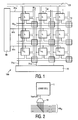
- Figure 1 shows a reconfigurable processing device 100 comprising one or more reconfigurable processing units 1.
- the units 1 may communicate to each other via a communication network comprising horizontal buses 90 H and vertical buses 90 V .
- the units 1 are connected to configuration bus CB, comprising an addres bus and a data bus and control signals for allowing configuration data to be loaded in a configuration memory which controls the functioning of the units 1.
- the reconfigurable processing device 100 comprises a first 60 and a second global decoder 70 which respectively activate a first control line, e.g. 61a and a second control line e.g. 71 b.
- the reconfigurable processing unit, here 1ab selected by the control lines is then reconfigured with the data from the configuration bus CB.
- the reconfigurable processing device 100 may only have local addres decoders.
- the reconfigurable processing device has no decoder at all, for example in an embodiment wherein the configuration storage units are arranged in a chain. In that case configuration takes place by subsequentially shifting the configuration data in the chain.
- Figure 2 shows an example wherein the multiplexer 13 selects an input signal from the signals available at a horizontal bus 90 H of the communication network.
- moLUTs Reconfigurable logic architectures with multi-bit output LUTs (moLUTs), have shown to offer multi-functionality at a reduced implementation cost.
- the most common way of implementing moLUTs is similar to traditional SRAMs, this is by using one decoder for addressing several (LUT) memory columns.
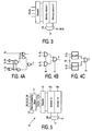
- a 4-input LUT is found to be the most area-efficient for random logic implementation. For that reason, a 4-input LUT is typically used in the implementation of the moLUT-based devices.
- the LUT type determines the total number of logic cell input pins. Thus, a device with a 4-input moLUT will have four pins. If an additional 2:1 multiplexer is placed at the LUT outputs, it will result in maximally five pins (see Fig. 3 ). This is not enough even to implement a 4:1 multiplexer, which requires six inputs (four primary and two selection inputs). Thus, typically only very small multiplexers can be implemented in such devices.
- Figure 4A, 4B, 4C show some prior art implementations of a multiplexer.
- Figure 4A shows a first approach, in which the multiplexer is implemented by dedicated circuitry.
- the multiplexer function is implemented by programming connections in a fixed topology of logic gates as well as by the selection of right operands for them (e.g. constants).
- the second approach is characteristic for the multiplexer-based devices as designed by Actel.
- a logic function is implemented by programming multiplexer inputs in a way required by the mapped function.
- the multiplexer-based reconfigurable logic devices are of a fine granularity and contain a small set of 2:1 multiplexers (usually three). Thus, maximally a 4:1 multiplexer can be implemented in such a structure.
- the third type of implementation as shown in Figure 4C assumes the use of look-up tables (LUTs), which is typical for most of the current FPGAs, e.g from Atmel and Xilinx.
- LUTs look-up tables
- look-up tables in a logic cell implement single multiplexers of the limited size (typically a 4:1 multiplexer), while wider multiplexers are created by using additional 2:1 multiplexers present at the look-up table outputs.
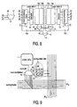
- FIG. 5 shows a computational unit in an embodiment of a reconfigurable processing device according to the invention.
- the basic idea behind the method proposed here is based on the decomposition of the multiplexer function in such a way, that it can be mapped onto the multi-bit output LUT which has been enhanced with a small amount of extra logic.
- this is shown for the implementation of a 4:1 multiplexer on the multi-bit output LUT with 4-inputs and 2-outputs (4/2-LUT).
- A is a function of the variables x 0 , x 2 , ..., x 2i and c 1 ,....c L
- B is a function of the variables x 1 , x 3 , ...x 2i+1 , and c 1 ,....c L
- the function A on its turn can be rewritten as the logical OR of the variables y 0 , y 2 , y 2i , wherein yi is a function which only depends on the variable xi and the selection variables c 1 ,....c L .
- the function B can be rewritten as the logical OR of the variables y 1 , y 3 , y 2i+1 , wherein yi is a function which only depends on the variable xi and the selection variables c 1 ,...c L .
- the functions y i can be calculated with a preprocessing unit, while the resulting function F is calculated from the values of yi and the remaining selection variables c 1 ,....c L .
- the preprocessing unit for generating the values y i is characterized in that the number n of input signals x i is equal to the number k of output signals y i and that the preprocessing unit has a first input for receiving a first selection signal c 1 , as well as further inputs for receiving the further selection signals c 2 ,...c L .
- the preprocessing unit generates in response to each of the input signals x i an output signal y i .
- the value is the logical AND function of the corresponding input signal xi and the first selection signal c 1 and for another half of the output signals y i the value is the logical AND function of the corresponding input signal x i and the inverse of the first selection signal c 1 .
- FIG. 6 shows a preprocessing unit 11 in a practical embodiment of the invention.
- the preprocessing unit comprises 4 logical AND gates 11a, 11b, 11c, 11d, and an inverter 11e to calculate the values y 0 , ...y 3 .
- the values y 0 and y 1 are realized by the logical AND function of their corresponding input signals x 0 , x 1 and the inverse of the first selection signal c 1 .
- the values y 2 and y 3 are realized by the logical AND function of their corresponding input signals x 2 , x 3 and first selection signal c 1 itself.
- the preprocessing module comprises a mode select input for selecting a further operational mode, in which further operational mode the output signals y i are identical to their corresponding input signals x i .
- the input processing block can be either bypassed Figure 7A or it can be used in such a way that the primary logic inputs are passed through it without any conversion.
- Figure 7A parts being referred to by reference numbers having a quote (') correspond to parts having the same reference number in Figure 6 .
- Figure 7B parts referred to by reference numbers having a double quote correspond to parts having a single quote in Figure 7A .
- each of the AND gates 11a', ... 11d' is coupled to an output via a respective auxiliary multiplexer 15a',...15d'.
- the multiplexers are coupled via a control input 17' of the preprocessing unit 11' to an output of the configuration memory 30'.
- the signal of the inverter 11e" is bypassed in the further operational mode.
- the auxiliary multiplexers 16a" and 16c" are coupled to control input 17" which is coupled to configuration memory 30".
- the auxiliary multiplexers select the logical value 1 as their output signals. The result is that each of the output signals y i is equal to x i .
- An additional advantage is that the auxiliary multiplexers 16a" and 16c" do not delay the signals y 0 , .. y 3 .
- Figure 8 shows a further embodiment of a reconfigurable processing device according to the invention claim 1. It comprises an enlarged computational unit having a first 10a and a second computational unit 10b. Each of the computational units 10a, 10b comprises a preprocessing module, a m-output look-up table, and an output multiplexer. In the embodiment shown the computational units 10a, 10b are identical to the one shown in Figure 5 .
- the enlarged computational unit shown in Figure 8 further comprises a further multiplexer 18 for selecting an output signal of either the first 10a or the second unit 10b as its output signal F in response to a further selection signal c2.
- Figure 9 shows a reconfigurable processing device wherein the computational unit 10 is arranged as an input multiplexer for a reconfigurable logic unit 1.
- the computational unit 10 selects an input signal for the reconfigurable logic unit 1 from signals available at a communication network 90 H , 90 V .
- the reconfigurable logic unit 1 has only one input, it may have a plurality of inputs. Each, or a paret of those inputs may be coupled to a computational unit 10 which is arranged as an input multiplexer.
- the selection signals for the computational unit 10 are provided by auxiliary computational units 20, 21, 22.
- Each auxiliary computational unit 20, 21, 22 selects either a signal from a configuration memory M2, M3 and M4 respectively or a signal from the communication network 90 V as its input signal. This selection is made in response to an auxiliary selection signal provided by the configuration memory M1.
Landscapes
- Physics & Mathematics (AREA)
- Engineering & Computer Science (AREA)
- Computer Hardware Design (AREA)
- Computing Systems (AREA)
- General Engineering & Computer Science (AREA)
- Mathematical Physics (AREA)
- Logic Circuits (AREA)
- Electronic Switches (AREA)
Abstract
Description
- The present invention relates to a reconfigurable processing device. Reconfigurable logic (RL) is used to implement functions which are unknown at the design time. To enable this reconfigurable logic architectures are made generic in the sense that various logic functions can be mapped onto them. Although this offers flexibility to a user, at the same time it leads to a large area overhead compared with the logic which would be required for a standard ASIC implementation, for example. Because of this, a basic computational element of traditional reconfigurable logic devices (such as field programmable gate arrays (FPGAs)), the so called logic cell, contains only a limited amount of logic resources, e.g. look-up tables. Moreover, the resources of a logic cell are chosen in such a way that they reflect the common requirements of different applications. However, if coarser or more specialised functions are to be mapped, usually either much more logic cells are required or such functions cannot be mapped at all.
- Reconfigurable logic devices comprise data flow controlling elements such as multiplexers, demultiplexers, gates etc and dataflow manipulating elements, such as logical gates, adders and lookup tables. The latter allow implementation of various functions, which can be redefined easily by loading them with a different content. Reconfigurable logic devices further comprise configuration memory units (configuration memory) for storing settings of data flow controlling elements, such as multiplexers, demultiplexers, switches etc. In this way connections between different parts of the reconfigurable processing unit can be rapidly redefined. Control signals for the memory cells are generated by an address decoder in response to an address offered at the input thereof.
- In particular multiplexers of different sizes and with different operand widths are heavily used in random logic as well as data-path applications. Despite that, in a large majority of traditional reconfigurable logic architectures, there is support for the implementation of small multiplexers only. This limitation has two reasons:
- 1. A specific type of a logic cell which hampers a multiplexer implementation.
- 2. A limited number of logic cell inputs which causes that a logic cell cannot obtain a required number of signals from the routing resources.
- For applications, in which wide multiplexers are heavily used (e.g. DSP data-paths, cryptography, networking), this is an important limitation. Although, this is particularly an issue for architectures with multi-bit output LUTs (moLUTs), any current FPGAs, both fine- and coarse-grained, face this problem in some way.
- It is an object of the invention to provide a reconfigurable processing device which allows for the implementation of relatively large multiplexers also in architectures using multi-bit output LUTs. In order to achieve this object the reconfigurable processing device is defined by
Claim 1. - In the reconfigurable processing device according to the invention, the preprocessing module reduces the number of signals, i.e. number n of input signals, and the number s1 of selection signals, to a smaller set of k output signals. The combination of the preprocessing module and the look-up table now can handle a relatively large number of input signals as compared to the look-up table alone.
- Preferably the look-up table is implemented according to the definition of
claim 2. This has the advantage that the decoder can be used both for writing and reading the table. The storage unit could also be used for temporarily storing data which is calculated in the reconfigurable processing device. - A practical embodiment is described in
claim 3. In this embodiment the preprocessing unit can have a relatively small number of gates. - The embodiment of claim 4 introduces additional flexibility to the reconfigurable device, in that it renders it possible to configure the computational unit either as a multiplexer, or as a general look-up table.
- Claim 5 provides an efficient way to implement an even wider multiplexer.
- These and other aspects of the invention are described in more detail with respect to the drawing. Therein:
-
Figure 1 schematically shows a reconfigurable processing device, -
Figure 2 shows in more detail the coupling between a reconfigurable processing unit and a communication network, -
Figure 3 shows a conventional element used in a reconfigurable processing device, -
Figure 4A, 4B and 4C shows three conventional approaches for implementing multiplexers in prior art reconfigurable devices, -
Figure 5 shows an embodiment according to the invention, -
Figure 6 shows an implementation of a preprocessing unit, -
Figure 7A and 7B show two alternative embodiments for the preprocessing unit, -
Figure 8 shows a further embodiment of the invention, -
Figure 9 shows a computational unit having an input multiplexer which is configurable statically or dynamically. -
Figure 1 shows areconfigurable processing device 100 comprising one or morereconfigurable processing units 1. Theunits 1 may communicate to each other via a communication network comprisinghorizontal buses 90H andvertical buses 90V. Theunits 1 are connected to configuration bus CB, comprising an addres bus and a data bus and control signals for allowing configuration data to be loaded in a configuration memory which controls the functioning of theunits 1. In the embodiment shown thereconfigurable processing device 100 comprises a first 60 and a secondglobal decoder 70 which respectively activate a first control line, e.g. 61a and a second control line e.g. 71 b. The reconfigurable processing unit, here 1ab selected by the control lines is then reconfigured with the data from the configuration bus CB. In another embodiment thereconfigurable processing device 100 may only have local addres decoders. In again another embodiment the reconfigurable processing device has no decoder at all, for example in an embodiment wherein the configuration storage units are arranged in a chain. In that case configuration takes place by subsequentially shifting the configuration data in the chain. - For many purposes it is necessary to select input signals for a
reconfigurable processing unit 1 from a plurality of signals available in the communication network.Figure 2 shows an example wherein themultiplexer 13 selects an input signal from the signals available at ahorizontal bus 90H of the communication network. - Reconfigurable logic architectures with multi-bit output LUTs (moLUTs), have shown to offer multi-functionality at a reduced implementation cost. The most common way of implementing moLUTs is similar to traditional SRAMs, this is by using one decoder for addressing several (LUT) memory columns. A 4-input LUT is found to be the most area-efficient for random logic implementation. For that reason, a 4-input LUT is typically used in the implementation of the moLUT-based devices. The LUT type determines the total number of logic cell input pins. Thus, a device with a 4-input moLUT will have four pins. If an additional 2:1 multiplexer is placed at the LUT outputs, it will result in maximally five pins (see
Fig. 3 ). This is not enough even to implement a 4:1 multiplexer, which requires six inputs (four primary and two selection inputs). Thus, typically only very small multiplexers can be implemented in such devices. -
Figure 4A, 4B, 4C show some prior art implementations of a multiplexer.Figure 4A shows a first approach, in which the multiplexer is implemented by dedicated circuitry. In such architectures the multiplexer function is implemented by programming connections in a fixed topology of logic gates as well as by the selection of right operands for them (e.g. constants). - The second approach, shown in
Figure 4B , is characteristic for the multiplexer-based devices as designed by Actel. In such devices, a logic function is implemented by programming multiplexer inputs in a way required by the mapped function. The multiplexer-based reconfigurable logic devices are of a fine granularity and contain a small set of 2:1 multiplexers (usually three). Thus, maximally a 4:1 multiplexer can be implemented in such a structure. - The third type of implementation as shown in
Figure 4C assumes the use of look-up tables (LUTs), which is typical for most of the current FPGAs, e.g from Atmel and Xilinx. - According to this approach, look-up tables in a logic cell implement single multiplexers of the limited size (typically a 4:1 multiplexer), while wider multiplexers are created by using additional 2:1 multiplexers present at the look-up table outputs.
-
Figure 5 shows a computational unit in an embodiment of a reconfigurable processing device according to the invention. Thecomputational unit 10 comprises apreprocessing module 11 for receiving n=4 input signals x0, x1, x2, x3, and s1=1 selection signals, signal c1 and providing k = 4 output signals y0, y1, y2, y3, wherein k < n+sl. It further comprises a m=2-output look-up table 12, 13a, 13b, being addressed by the k output signals of the preprocessing module, and anoutput multiplexer 14 for selecting one of the m=2 output signals of the look-up table 12, 13a, 13b under control of s2=1 further selection signals as the output signal F. - The basic idea behind the method proposed here is based on the decomposition of the multiplexer function in such a way, that it can be mapped onto the multi-bit output LUT which has been enhanced with a small amount of extra logic. By way of example, this is shown for the implementation of a 4:1 multiplexer on the multi-bit output LUT with 4-inputs and 2-outputs (4/2-LUT).
- A 4:1 multiplexer can be described by a logic function F of six variables: x0,x1,x2,x3, being inputs of the multiplexer and c0,c1 being control (selection) signals, as shown by the
following equation:
This equation can be further modified to the form:
wherein:
and
Eqn 2 describes a 2:1 multiplexer with inputs A, B, and c0 being a control signal. This multiplexer can be mapped onto the 2:1 multiplexer which is present at the outputs of the 4/2-LUT. Such a mapping is possible only if both functions A and B can be encoded in the memories (memory columns) of the moLUT. Functions A and B require in total five different logic variables while the given 4/2-LUT has only four inputs. However, all partial products of the A and B functions share the same logic variable c1. If it is assumed that these partial productsc 1 .x 0,c 1 , x 1, c 1 x 2, c 1 x 3 are generated outside the LUT, than the partial product results y0, y1, y2, y3 can be treated as inputs of this LUT. Thus, a 4/2-LUT implements functions A and B of the form as in Eqn. 4
and
- The only modification required with respect to the standard 4/2-LUT implementation is a relatively
small preprocessing unit 11. - The above described principle is not limited to the implementation of 4:2 multiplexers. Analogously any selection function F:


- Likewise the function B can be rewritten as the logical OR of the variables y1, y3, y2i+1, wherein yi is a function which only depends on the variable xi and the selection variables c1,...cL. Again, the functions yi can be calculated with a preprocessing unit, while the resulting function F is calculated from the values of yi and the remaining selection variables c1,....cL.
- The preprocessing unit for generating the values yi is characterized in that the number n of input signals xi is equal to the number k of output signals yi and that the preprocessing unit has a first input for receiving a first selection signal c1, as well as further inputs for receiving the further selection signals c2,...cL. The preprocessing unit generates in response to each of the input signals xi an output signal yi. For one half of the output signals yi the value is the logical AND function of the corresponding input signal xi and the first selection signal c1 and for another half of the output signals yi the value is the logical AND function of the corresponding input signal xi and the inverse of the first selection signal c1.
- By way of example
Figure 6 shows apreprocessing unit 11 in a practical embodiment of the invention. The preprocessing unit comprises 4 logical ANDgates inverter 11e to calculate the values y0, ...y3. The values y0 and y1 are realized by the logical AND function of their corresponding input signals x0, x1 and the inverse of the first selection signal c1. The values y2 and y3 are realized by the logical AND function of their corresponding input signals x2, x3 and first selection signal c1 itself. - Preferably the preprocessing module comprises a mode select input for selecting a further operational mode, in which further operational mode the output signals yi are identical to their corresponding input signals xi. If a logic function of only four inputs is to be implemented in the modified 4/2-LUT, than the input processing block can be either bypassed
Figure 7A or it can be used in such a way that the primary logic inputs are passed through it without any conversion. InFigure 7A parts being referred to by reference numbers having a quote (') correspond to parts having the same reference number inFigure 6 . InFigure 7B parts referred to by reference numbers having a double quote correspond to parts having a single quote inFigure 7A . - In the embodiment shown in
Figure 7A each of the ANDgates 11a', ... 11d' is coupled to an output via a respectiveauxiliary multiplexer 15a',...15d'. The multiplexers are coupled via a control input 17' of the preprocessing unit 11' to an output of the configuration memory 30'. - In the embodiment of
Figure 7B the signal of theinverter 11e" is bypassed in the further operational mode. To that end the auxiliary multiplexers 16a" and 16c" are coupled to controlinput 17" which is coupled toconfiguration memory 30". In the further operational mode the auxiliary multiplexers select thelogical value 1 as their output signals. The result is that each of the output signals yi is equal to xi. An additional advantage is that the auxiliary multiplexers 16a" and 16c" do not delay the signals y0, .. y3. -
Figure 8 shows a further embodiment of a reconfigurable processing device according to theinvention claim 1. It comprises an enlarged computational unit having a first 10a and a secondcomputational unit 10b. Each of thecomputational units computational units Figure 5 . The enlarged computational unit shown inFigure 8 further comprises afurther multiplexer 18 for selecting an output signal of either the first 10a or thesecond unit 10b as its output signal F in response to a further selection signal c2. -
Figure 9 shows a reconfigurable processing device wherein thecomputational unit 10 is arranged as an input multiplexer for areconfigurable logic unit 1. Thecomputational unit 10 selects an input signal for thereconfigurable logic unit 1 from signals available at acommunication network Figure 9 thereconfigurable logic unit 1 has only one input, it may have a plurality of inputs. Each, or a paret of those inputs may be coupled to acomputational unit 10 which is arranged as an input multiplexer. - In the embodiment shown in
Figure 9 the selection signals for thecomputational unit 10 are provided by auxiliarycomputational units computational unit communication network 90V as its input signal. This selection is made in response to an auxiliary selection signal provided by the configuration memory M1. - It is remarked that the scope of protection of the invention is not restricted to the embodiments described herein. Neither is the scope of protection of the invention restricted by the reference numerals in the claims. The word 'comprising' does not exclude other parts than those mentioned in a claim. The word 'a(n)' preceding an element does not exclude a plurality of those elements. Means forming part of the invention may both be implemented in the form of dedicated hardware or in the form of a programmed general purpose processor. The invention resides in each new feature or combination of features.
Claims (5)
- Reconfigurable processing device (100) comprising one or more reconfigurable processing units (1) including a:camputational unit (10) having- a preprocessing module (11) for receiving n input signals (X0,..X3), and s1 selection signals (c1), and providing k output signals (y0, ... y1) wherein k < n+s1,- a m-output look-up table (12, 13a, 13b) being addressed by the k output signals of the preprocessing module (11),- an output multiplexer (14) for selecting one of the m output signals of the look-up table (12, 13a, 13b) under control of s2 further selection signals (c0).
- Reconfigurable processing device according to claim 1, characterized in that the look-up table includes a k:2k decoder (12) for decoding k address signals (y0,...y3) into 2k control signals and a storage unit (13a, 13b) comprising m columns of 2k storage elements each.
- Reconfigurable processing device according to claim 1, characterized in that n = k and that the preprocessing unit (11) has a first input for receiving a first selection signal (c1), wherein the preprocessing unit (11) in an operational mode generates in response to each of the input signals (xi) an output signal (yi) wherein for one half of the output signals (y2, y3) the value is the logical AND function of the corresponding input signal (x2, x3 resp.) and the first selection signal (c1) and for another half of the output signals (y0, y1) the value is the logical AND function of the corresponding input signal (x0, x1 resp.) and the inverse of the first selection signal (c1).
- Reconfigurable processing device according to claim 3, characterized in that the preprocessing unit (11';11") comprises a mode select input (17', 17") for selecting a further operational mode, in which further operational mode the output signals (yi) are identical to their corresponding input signals (xi).
- Reconfigurable processing device according to claim 1, characterized in that it comprises an enlarged computational unit having a first and a second computational unit (10a, 10b) comprising each a preprocessing module (11), a m-output look-up table (12, 13a, 13b), and an output multiplexer (14), the enlarged computational unit further comprising a further multiplexer (18) for selecting an output signal of either the first or the second unit (10a, 10b) as its output signal (F) in response to a further selection signal (c2).
Priority Applications (1)
| Application Number | Priority Date | Filing Date | Title |
|---|---|---|---|
| EP03744472A EP1488523B1 (en) | 2002-03-18 | 2003-03-17 | Implementation of wide multiplexers in reconfigurable logic |
Applications Claiming Priority (4)
| Application Number | Priority Date | Filing Date | Title |
|---|---|---|---|
| EP02076049 | 2002-03-18 | ||
| EP02076049 | 2002-03-18 | ||
| EP03744472A EP1488523B1 (en) | 2002-03-18 | 2003-03-17 | Implementation of wide multiplexers in reconfigurable logic |
| PCT/IB2003/000967 WO2003079550A2 (en) | 2002-03-18 | 2003-03-17 | Implementation of wide multiplexers in reconfigurable logic |
Publications (2)
| Publication Number | Publication Date |
|---|---|
| EP1488523A2 EP1488523A2 (en) | 2004-12-22 |
| EP1488523B1 true EP1488523B1 (en) | 2010-02-17 |
Family
ID=27838094
Family Applications (1)
| Application Number | Title | Priority Date | Filing Date |
|---|---|---|---|
| EP03744472A Expired - Lifetime EP1488523B1 (en) | 2002-03-18 | 2003-03-17 | Implementation of wide multiplexers in reconfigurable logic |
Country Status (8)
| Country | Link |
|---|---|
| US (1) | US8082284B2 (en) |
| EP (1) | EP1488523B1 (en) |
| JP (1) | JP4260026B2 (en) |
| CN (1) | CN1295879C (en) |
| AT (1) | ATE458310T1 (en) |
| AU (1) | AU2003209576A1 (en) |
| DE (1) | DE60331296D1 (en) |
| WO (1) | WO2003079550A2 (en) |
Families Citing this family (6)
| Publication number | Priority date | Publication date | Assignee | Title |
|---|---|---|---|---|
| DE102004045527B4 (en) | 2003-10-08 | 2009-12-03 | Siemens Ag | Configurable logic circuitry |
| CN102147720B (en) * | 2011-03-18 | 2014-04-09 | 深圳市国微电子有限公司 | Device and method for realizing operation among multiple input logical terms by using LUT |
| US9450585B2 (en) * | 2011-04-20 | 2016-09-20 | Microchip Technology Incorporated | Selecting four signals from sixteen inputs |
| JPWO2014163099A1 (en) * | 2013-04-02 | 2017-02-16 | 太陽誘電株式会社 | Reconfigurable logical device |
| US9954533B2 (en) * | 2014-12-16 | 2018-04-24 | Samsung Electronics Co., Ltd. | DRAM-based reconfigurable logic |
| JP6653126B2 (en) * | 2015-04-28 | 2020-02-26 | 太陽誘電株式会社 | Reconfigurable semiconductor device |
Family Cites Families (16)
| Publication number | Priority date | Publication date | Assignee | Title |
|---|---|---|---|---|
| US5225719A (en) * | 1985-03-29 | 1993-07-06 | Advanced Micro Devices, Inc. | Family of multiple segmented programmable logic blocks interconnected by a high speed centralized switch matrix |
| US5233539A (en) * | 1989-08-15 | 1993-08-03 | Advanced Micro Devices, Inc. | Programmable gate array with improved interconnect structure, input/output structure and configurable logic block |
| US5498975A (en) * | 1992-11-19 | 1996-03-12 | Altera Corporation | Implementation of redundancy on a programmable logic device |
| JP3127654B2 (en) * | 1993-03-12 | 2001-01-29 | 株式会社デンソー | Multiplier / divider |
| JPH06276086A (en) * | 1993-03-18 | 1994-09-30 | Fuji Xerox Co Ltd | Field programmable gate array |
| US5426379A (en) * | 1994-07-29 | 1995-06-20 | Xilinx, Inc. | Field programmable gate array with built-in bitstream data expansion |
| US5442306A (en) | 1994-09-09 | 1995-08-15 | At&T Corp. | Field programmable gate array using look-up tables, multiplexers and decoders |
| JPH09181598A (en) | 1995-12-18 | 1997-07-11 | At & T Corp | Field programmable gate array |
| US6154049A (en) * | 1998-03-27 | 2000-11-28 | Xilinx, Inc. | Multiplier fabric for use in field programmable gate arrays |
| US6567834B1 (en) * | 1997-12-17 | 2003-05-20 | Elixent Limited | Implementation of multipliers in programmable arrays |
| GB9727414D0 (en) * | 1997-12-29 | 1998-02-25 | Imperial College | Logic circuit |
| JP3123977B2 (en) * | 1998-06-04 | 2001-01-15 | 日本電気株式会社 | Programmable function block |
| US6118300A (en) * | 1998-11-24 | 2000-09-12 | Xilinx, Inc. | Method for implementing large multiplexers with FPGA lookup tables |
| JP3269526B2 (en) * | 1999-02-09 | 2002-03-25 | 日本電気株式会社 | Programmable logic LSI |
| US6556042B1 (en) * | 2002-02-20 | 2003-04-29 | Xilinx, Inc. | FPGA with improved structure for implementing large multiplexers |
| US6816562B2 (en) * | 2003-01-07 | 2004-11-09 | Mathstar, Inc. | Silicon object array with unidirectional segmented bus architecture |
-
2003
- 2003-03-17 AT AT03744472T patent/ATE458310T1/en not_active IP Right Cessation
- 2003-03-17 EP EP03744472A patent/EP1488523B1/en not_active Expired - Lifetime
- 2003-03-17 AU AU2003209576A patent/AU2003209576A1/en not_active Abandoned
- 2003-03-17 US US10/507,807 patent/US8082284B2/en not_active Expired - Fee Related
- 2003-03-17 CN CNB038061848A patent/CN1295879C/en not_active Expired - Fee Related
- 2003-03-17 DE DE60331296T patent/DE60331296D1/en not_active Expired - Lifetime
- 2003-03-17 JP JP2003577426A patent/JP4260026B2/en not_active Expired - Fee Related
- 2003-03-17 WO PCT/IB2003/000967 patent/WO2003079550A2/en active Application Filing
Also Published As
| Publication number | Publication date |
|---|---|
| EP1488523A2 (en) | 2004-12-22 |
| DE60331296D1 (en) | 2010-04-01 |
| JP2005521288A (en) | 2005-07-14 |
| US20050232297A1 (en) | 2005-10-20 |
| AU2003209576A1 (en) | 2003-09-29 |
| US8082284B2 (en) | 2011-12-20 |
| WO2003079550A3 (en) | 2004-03-04 |
| JP4260026B2 (en) | 2009-04-30 |
| ATE458310T1 (en) | 2010-03-15 |
| CN1295879C (en) | 2007-01-17 |
| CN1643793A (en) | 2005-07-20 |
| WO2003079550A2 (en) | 2003-09-25 |
Similar Documents
| Publication | Publication Date | Title |
|---|---|---|
| US5818255A (en) | Method and circuit for using a function generator of a programmable logic device to implement carry logic functions | |
| US5570039A (en) | Programmable function unit as parallel multiplier cell | |
| US6271680B1 (en) | Logic element for a programmable logic integrated circuit | |
| US7317330B2 (en) | Logic circuitry with shared lookup table | |
| US7251672B2 (en) | Reconfigurable logic device | |
| US7088134B1 (en) | Programmable logic device with flexible memory allocation and routing | |
| JP2006519548A (en) | Electronic circuit with an array of programmable logic cells. | |
| US10560102B1 (en) | Field programmable gate array including coupled lookup tables | |
| US6873182B2 (en) | Programmable logic devices having enhanced cascade functions to provide increased flexibility | |
| JPH06266750A (en) | Logic system | |
| US8581624B2 (en) | Integrated circuits with multi-stage logic regions | |
| KR101067727B1 (en) | Electronic circuit with array of programmable logic cells | |
| US6255846B1 (en) | Programmable logic devices with enhanced multiplexing capabilities | |
| US7185035B1 (en) | Arithmetic structures for programmable logic devices | |
| JP2006518144A (en) | Electronic circuit with an array of programmable logic cells. | |
| US6961741B2 (en) | Look-up table apparatus to perform two-bit arithmetic operation including carry generation | |
| EP1488523B1 (en) | Implementation of wide multiplexers in reconfigurable logic | |
| US20060097750A1 (en) | Electronic circuit with array of programmable logic cells | |
| US8041925B2 (en) | Switch coupled function blocks with additional direct coupling and internal data passing from input to output to facilitate more switched inputs to second block | |
| US6356110B1 (en) | Multifunction memory array in a programmable logic device | |
| US7467124B2 (en) | Arrangement of configurable logic blocks | |
| JPH05252024A (en) | Programmable logic cell | |
| JPH0644710B2 (en) | Logical elements with configurable configurations | |
| JPH09121153A (en) | Programmable logic element |
Legal Events
| Date | Code | Title | Description |
|---|---|---|---|
| PUAI | Public reference made under article 153(3) epc to a published international application that has entered the european phase |
Free format text: ORIGINAL CODE: 0009012 |
|
| 17P | Request for examination filed |
Effective date: 20041018 |
|
| AK | Designated contracting states |
Kind code of ref document: A2 Designated state(s): AT BE BG CH CY CZ DE DK EE ES FI FR GB GR HU IE IT LI LU MC NL PT RO SE SI SK TR |
|
| AX | Request for extension of the european patent |
Extension state: AL LT LV MK |
|
| RAP1 | Party data changed (applicant data changed or rights of an application transferred) |
Owner name: NXP B.V. |
|
| GRAP | Despatch of communication of intention to grant a patent |
Free format text: ORIGINAL CODE: EPIDOSNIGR1 |
|
| GRAS | Grant fee paid |
Free format text: ORIGINAL CODE: EPIDOSNIGR3 |
|
| GRAA | (expected) grant |
Free format text: ORIGINAL CODE: 0009210 |
|
| AK | Designated contracting states |
Kind code of ref document: B1 Designated state(s): AT BE BG CH CY CZ DE DK EE ES FI FR GB GR HU IE IT LI LU MC NL PT RO SE SI SK TR |
|
| REG | Reference to a national code |
Ref country code: GB Ref legal event code: FG4D |
|
| REG | Reference to a national code |
Ref country code: CH Ref legal event code: EP |
|
| REG | Reference to a national code |
Ref country code: IE Ref legal event code: FG4D |
|
| REF | Corresponds to: |
Ref document number: 60331296 Country of ref document: DE Date of ref document: 20100401 Kind code of ref document: P |
|
| REG | Reference to a national code |
Ref country code: NL Ref legal event code: VDEP Effective date: 20100217 |
|
| PG25 | Lapsed in a contracting state [announced via postgrant information from national office to epo] |
Ref country code: PT Free format text: LAPSE BECAUSE OF FAILURE TO SUBMIT A TRANSLATION OF THE DESCRIPTION OR TO PAY THE FEE WITHIN THE PRESCRIBED TIME-LIMIT Effective date: 20100617 Ref country code: ES Free format text: LAPSE BECAUSE OF FAILURE TO SUBMIT A TRANSLATION OF THE DESCRIPTION OR TO PAY THE FEE WITHIN THE PRESCRIBED TIME-LIMIT Effective date: 20100528 |
|
| PG25 | Lapsed in a contracting state [announced via postgrant information from national office to epo] |
Ref country code: SI Free format text: LAPSE BECAUSE OF FAILURE TO SUBMIT A TRANSLATION OF THE DESCRIPTION OR TO PAY THE FEE WITHIN THE PRESCRIBED TIME-LIMIT Effective date: 20100217 Ref country code: AT Free format text: LAPSE BECAUSE OF FAILURE TO SUBMIT A TRANSLATION OF THE DESCRIPTION OR TO PAY THE FEE WITHIN THE PRESCRIBED TIME-LIMIT Effective date: 20100217 Ref country code: FI Free format text: LAPSE BECAUSE OF FAILURE TO SUBMIT A TRANSLATION OF THE DESCRIPTION OR TO PAY THE FEE WITHIN THE PRESCRIBED TIME-LIMIT Effective date: 20100217 |
|
| PG25 | Lapsed in a contracting state [announced via postgrant information from national office to epo] |
Ref country code: SE Free format text: LAPSE BECAUSE OF FAILURE TO SUBMIT A TRANSLATION OF THE DESCRIPTION OR TO PAY THE FEE WITHIN THE PRESCRIBED TIME-LIMIT Effective date: 20100217 Ref country code: BE Free format text: LAPSE BECAUSE OF FAILURE TO SUBMIT A TRANSLATION OF THE DESCRIPTION OR TO PAY THE FEE WITHIN THE PRESCRIBED TIME-LIMIT Effective date: 20100217 Ref country code: CY Free format text: LAPSE BECAUSE OF FAILURE TO SUBMIT A TRANSLATION OF THE DESCRIPTION OR TO PAY THE FEE WITHIN THE PRESCRIBED TIME-LIMIT Effective date: 20100217 Ref country code: EE Free format text: LAPSE BECAUSE OF FAILURE TO SUBMIT A TRANSLATION OF THE DESCRIPTION OR TO PAY THE FEE WITHIN THE PRESCRIBED TIME-LIMIT Effective date: 20100217 Ref country code: GR Free format text: LAPSE BECAUSE OF FAILURE TO SUBMIT A TRANSLATION OF THE DESCRIPTION OR TO PAY THE FEE WITHIN THE PRESCRIBED TIME-LIMIT Effective date: 20100518 Ref country code: MC Free format text: LAPSE BECAUSE OF NON-PAYMENT OF DUE FEES Effective date: 20100331 Ref country code: NL Free format text: LAPSE BECAUSE OF FAILURE TO SUBMIT A TRANSLATION OF THE DESCRIPTION OR TO PAY THE FEE WITHIN THE PRESCRIBED TIME-LIMIT Effective date: 20100217 Ref country code: RO Free format text: LAPSE BECAUSE OF FAILURE TO SUBMIT A TRANSLATION OF THE DESCRIPTION OR TO PAY THE FEE WITHIN THE PRESCRIBED TIME-LIMIT Effective date: 20100217 |
|
| REG | Reference to a national code |
Ref country code: CH Ref legal event code: PL |
|
| PG25 | Lapsed in a contracting state [announced via postgrant information from national office to epo] |
Ref country code: SK Free format text: LAPSE BECAUSE OF FAILURE TO SUBMIT A TRANSLATION OF THE DESCRIPTION OR TO PAY THE FEE WITHIN THE PRESCRIBED TIME-LIMIT Effective date: 20100217 Ref country code: CZ Free format text: LAPSE BECAUSE OF FAILURE TO SUBMIT A TRANSLATION OF THE DESCRIPTION OR TO PAY THE FEE WITHIN THE PRESCRIBED TIME-LIMIT Effective date: 20100217 Ref country code: BG Free format text: LAPSE BECAUSE OF FAILURE TO SUBMIT A TRANSLATION OF THE DESCRIPTION OR TO PAY THE FEE WITHIN THE PRESCRIBED TIME-LIMIT Effective date: 20100517 |
|
| PLBE | No opposition filed within time limit |
Free format text: ORIGINAL CODE: 0009261 |
|
| STAA | Information on the status of an ep patent application or granted ep patent |
Free format text: STATUS: NO OPPOSITION FILED WITHIN TIME LIMIT |
|
| 26N | No opposition filed |
Effective date: 20101118 |
|
| PG25 | Lapsed in a contracting state [announced via postgrant information from national office to epo] |
Ref country code: IE Free format text: LAPSE BECAUSE OF NON-PAYMENT OF DUE FEES Effective date: 20100317 Ref country code: DK Free format text: LAPSE BECAUSE OF FAILURE TO SUBMIT A TRANSLATION OF THE DESCRIPTION OR TO PAY THE FEE WITHIN THE PRESCRIBED TIME-LIMIT Effective date: 20100217 |
|
| PG25 | Lapsed in a contracting state [announced via postgrant information from national office to epo] |
Ref country code: CH Free format text: LAPSE BECAUSE OF NON-PAYMENT OF DUE FEES Effective date: 20100331 Ref country code: LI Free format text: LAPSE BECAUSE OF NON-PAYMENT OF DUE FEES Effective date: 20100331 |
|
| PG25 | Lapsed in a contracting state [announced via postgrant information from national office to epo] |
Ref country code: IT Free format text: LAPSE BECAUSE OF FAILURE TO SUBMIT A TRANSLATION OF THE DESCRIPTION OR TO PAY THE FEE WITHIN THE PRESCRIBED TIME-LIMIT Effective date: 20100217 |
|
| PG25 | Lapsed in a contracting state [announced via postgrant information from national office to epo] |
Ref country code: HU Free format text: LAPSE BECAUSE OF FAILURE TO SUBMIT A TRANSLATION OF THE DESCRIPTION OR TO PAY THE FEE WITHIN THE PRESCRIBED TIME-LIMIT Effective date: 20100818 Ref country code: LU Free format text: LAPSE BECAUSE OF NON-PAYMENT OF DUE FEES Effective date: 20100317 |
|
| PG25 | Lapsed in a contracting state [announced via postgrant information from national office to epo] |
Ref country code: TR Free format text: LAPSE BECAUSE OF FAILURE TO SUBMIT A TRANSLATION OF THE DESCRIPTION OR TO PAY THE FEE WITHIN THE PRESCRIBED TIME-LIMIT Effective date: 20100217 |
|
| REG | Reference to a national code |
Ref country code: FR Ref legal event code: PLFP Year of fee payment: 14 |
|
| REG | Reference to a national code |
Ref country code: FR Ref legal event code: PLFP Year of fee payment: 15 |
|
| REG | Reference to a national code |
Ref country code: DE Ref legal event code: R082 Ref document number: 60331296 Country of ref document: DE Representative=s name: GRUENECKER PATENT- UND RECHTSANWAELTE PARTG MB, DE Ref country code: DE Ref legal event code: R081 Ref document number: 60331296 Country of ref document: DE Owner name: OCT CIRCUIT TECHNOLOGIES INTERNATIONAL LTD., IE Free format text: FORMER OWNER: NXP B.V., EINDHOVEN, NL |
|
| PGFP | Annual fee paid to national office [announced via postgrant information from national office to epo] |
Ref country code: FR Payment date: 20170221 Year of fee payment: 15 Ref country code: DE Payment date: 20170222 Year of fee payment: 15 |
|
| PGFP | Annual fee paid to national office [announced via postgrant information from national office to epo] |
Ref country code: GB Payment date: 20170224 Year of fee payment: 15 |
|
| REG | Reference to a national code |
Ref country code: DE Ref legal event code: R119 Ref document number: 60331296 Country of ref document: DE |
|
| GBPC | Gb: european patent ceased through non-payment of renewal fee |
Effective date: 20180317 |
|
| PG25 | Lapsed in a contracting state [announced via postgrant information from national office to epo] |
Ref country code: DE Free format text: LAPSE BECAUSE OF NON-PAYMENT OF DUE FEES Effective date: 20181002 |
|
| PG25 | Lapsed in a contracting state [announced via postgrant information from national office to epo] |
Ref country code: GB Free format text: LAPSE BECAUSE OF NON-PAYMENT OF DUE FEES Effective date: 20180317 |
|
| PG25 | Lapsed in a contracting state [announced via postgrant information from national office to epo] |
Ref country code: FR Free format text: LAPSE BECAUSE OF NON-PAYMENT OF DUE FEES Effective date: 20180331 |