EP1486784A2 - Sensor with alignment self-compensation - Google Patents
Sensor with alignment self-compensation Download PDFInfo
- Publication number
- EP1486784A2 EP1486784A2 EP04102631A EP04102631A EP1486784A2 EP 1486784 A2 EP1486784 A2 EP 1486784A2 EP 04102631 A EP04102631 A EP 04102631A EP 04102631 A EP04102631 A EP 04102631A EP 1486784 A2 EP1486784 A2 EP 1486784A2
- Authority
- EP
- European Patent Office
- Prior art keywords
- radiation source
- signals
- sensor
- material web
- calibration constant
- Prior art date
- Legal status (The legal status is an assumption and is not a legal conclusion. Google has not performed a legal analysis and makes no representation as to the accuracy of the status listed.)
- Granted
Links
Images


Classifications
-
- G—PHYSICS
- G01—MEASURING; TESTING
- G01N—INVESTIGATING OR ANALYSING MATERIALS BY DETERMINING THEIR CHEMICAL OR PHYSICAL PROPERTIES
- G01N33/00—Investigating or analysing materials by specific methods not covered by groups G01N1/00 - G01N31/00
- G01N33/36—Textiles
- G01N33/367—Fabric or woven textiles
-
- G—PHYSICS
- G01—MEASURING; TESTING
- G01N—INVESTIGATING OR ANALYSING MATERIALS BY DETERMINING THEIR CHEMICAL OR PHYSICAL PROPERTIES
- G01N23/00—Investigating or analysing materials by the use of wave or particle radiation, e.g. X-rays or neutrons, not covered by groups G01N3/00 – G01N17/00, G01N21/00 or G01N22/00
- G01N23/02—Investigating or analysing materials by the use of wave or particle radiation, e.g. X-rays or neutrons, not covered by groups G01N3/00 – G01N17/00, G01N21/00 or G01N22/00 by transmitting the radiation through the material
- G01N23/06—Investigating or analysing materials by the use of wave or particle radiation, e.g. X-rays or neutrons, not covered by groups G01N3/00 – G01N17/00, G01N21/00 or G01N22/00 by transmitting the radiation through the material and measuring the absorption
- G01N23/16—Investigating or analysing materials by the use of wave or particle radiation, e.g. X-rays or neutrons, not covered by groups G01N3/00 – G01N17/00, G01N21/00 or G01N22/00 by transmitting the radiation through the material and measuring the absorption the material being a moving sheet or film
-
- G—PHYSICS
- G01—MEASURING; TESTING
- G01N—INVESTIGATING OR ANALYSING MATERIALS BY DETERMINING THEIR CHEMICAL OR PHYSICAL PROPERTIES
- G01N23/00—Investigating or analysing materials by the use of wave or particle radiation, e.g. X-rays or neutrons, not covered by groups G01N3/00 – G01N17/00, G01N21/00 or G01N22/00
- G01N23/02—Investigating or analysing materials by the use of wave or particle radiation, e.g. X-rays or neutrons, not covered by groups G01N3/00 – G01N17/00, G01N21/00 or G01N22/00 by transmitting the radiation through the material
- G01N23/06—Investigating or analysing materials by the use of wave or particle radiation, e.g. X-rays or neutrons, not covered by groups G01N3/00 – G01N17/00, G01N21/00 or G01N22/00 by transmitting the radiation through the material and measuring the absorption
- G01N23/083—Investigating or analysing materials by the use of wave or particle radiation, e.g. X-rays or neutrons, not covered by groups G01N3/00 – G01N17/00, G01N21/00 or G01N22/00 by transmitting the radiation through the material and measuring the absorption the radiation being X-rays
Definitions
- the present invention relates to the measurement of material web characteristics, and, more particularly, to sensors used in the measurement of material web characteristics.
- a radiation source In measuring a basis weight, moisture or thickness, or other characteristics, of a moving material web a radiation source is mounted on one side of the web material and on the other side is a receiving transducer. The source/transducer pair are then scanned in a cross direction (perpendicular to the movement or machine direction of the web material) to provide a cross direction measurement of that particular characteristic.
- any uncompensated variation in the size of the measuring gap will cause an error in the measurement.
- these errors were compensated either by using a separate sensor to measure the gap size, with additional references and the like or by shaping the radiation beam so that the sensitivity to alignment errors were minimized.
- the disadvantage of using separate sensors or additional references to measure the gap size is the increase in cost and complexity, and a corresponding decrease in reliability, associated with the additional equipment.
- the disadvantage in shaping the beam is the associated reduction in signal strength leads to a reduction in the signal to noise ratio.
- U.S. Patent No. 5,233,195 discloses methods and apparatus for measuring characteristics of moving webs wherein alignment insensitivity is obtained by tuning the radiation beam using concentric rings or crossed strips of material which is semitransparent to the radiation to compensate for geometric characteristics of the radiation source/beam and the detector.
- U.S. Patent No. 5,010,766 discloses error compensation for measuring gauges by the use of two pairs of eddy current sensors which are centered on a target on the opposed transducer head and which sense the pairs of edges of an aperture in the opposed transducer.
- U.S. Patent No. 4,678,915 discloses a system for measuring the values of a parameter of a web of material including a head system with sensors mounted therein and a separate distance correction system.
- U.S. Patent No. 4,276,480 discloses a sensor response indicative of a distance which can be related to a thickness property of a material by a procedure that includes establishing a reference position, such as to a support, and locating the material precisely in a predetermined spatial relation to the reference position.
- the present invention provides a sensor for detecting web qualities which is self compensating with respect to the sensor alignment.
- the invention comprises, in one form thereof, a material web attribute detection system with the material web having a first side and a second side.
- the system includes a radiation source located proximate to the first side of the material web and emitting radiation toward the material web, and a radiation detection array located proximate to the second side of the material web and producing a plurality of signals based on the radiation detected from the radiation source.
- a processor is included which utilizes the plurality of signals to determine a lateral offset and a gap size of the radiation detection array relative to the radiation source. The processor can then compensate for the radiation detection array and radiation source relative misalignment using the plurality of signals, the lateral offset and the gap size.
- An advantage of the present invention is that it provides a method and apparatus to compensate sensors for misalignment over a wide range.
- Another advantage of the present invention is that the sensor can be optimized mathematically with greater accuracy than what has been possible with the prior art.
- Yet another advantage of the present invention is that it does not require additional sensor elements for alignment compensation.
- a further advantage of the present invention is that it does not require additional reference elements for alignment compensation.
- a further advantage of the present invention is that it does not require radiation beam shaping for alignment compensation.
- a material web attribute detection system 10 of the present invention including radiation source 12, source aperture and window 14, radiation beam 16, material web 18, receiver window 20, detector or sensor array 22 and processor 24.
- Radiation source 12 generates radioactive particles and/or electromagnetic energy. Radiation source 12 can be surrounded by a radiation absorbing or reflecting material with an opening on one side to thereby mainly emit radiation from one side of radiation source 12. Radiation source 12 can, for example, emit primarily beta particles or x-rays but is not limited to such particle or energy emission. Alternatively, radiation source 12 can emit in any range of the electromagnetic spectrum including radio, microwave, infrared, ultraviolet, gamma ray and cosmic ray spectral ranges, and higher energy atomic and subatomic particles. Source aperture and window 14 includes aperture 26 through which radiation emitted by radiation source 12 can pass through. Aperture 26 can be closed and opened under command of processor 24 or another control mechanism (not shown). Source aperture and window 14 is generally positionally and angularly fixed with respect to radiation source 12. Alternatively, source aperture and window 14 are adjustable.
- Material web 18 is suspended between detector array 22 and the combination radiation source 12 and source aperture and window 14. Gap 30, between source aperture and window 14 and detector window 20, is sufficiently wide that material web 18 does not touch either source aperture 14 or detector window 20.
- Material web 18 is typically a moving web of material such as paper, cardboard or a plastic. Material web has a machine direction (MD) and a cross-machine direction (CD).
- detector array 22 is positioned in substantial alignment with radiation source 12 to thereby centrally locate sensor S22, so as to be substantially centered in radiation beam 16 as shown in Figs. 1 and 5.
- the peak intensity of radiation beam 16, as represented in Fig. 5, is substantially directed toward sensor S22. While a substantial alignment of radiation beam 16 is desired, the present invention determines and compensates for any misalignment.
- Receiver window 20 is generally positionally and angularly fixed with respect to detector array 22. Alternatively, receiver window 20 is adjustable.
- Fig. 1 shows radiation source 12 in substantial relative alignment with detector array 22.
- Fig. 5 shows nominal beam projection 32 on detector array 22 resulting from the alignment shown in Fig. 1.
- Fig. 6 shows radiation source 12 in Z direction, or gap, misalignment with detector array 22.
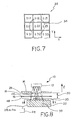
- Fig. 7 shows beam projection 34 broadened on detector array 22 with gap misalignment resulting from the misalignment shown in Fig. 6.
- Fig. 8 shows radiation source 12 in lateral, or X,Y direction misalignment with detector array 22.
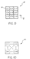
- Fig. 9 shows beam projection 36 offset on detector array 22 resulting from the misalignment shown in Fig. 8.
- Radiation beam 16 (wave, particle or combination thereof), from radiation source 12, propagates through source aperture and window 14, material web 18 and detector window 20 to arrive at detector array 22.
- Detector window 20 is substantially transparent to the radiation and may include an antireflective coating similar to source aperture and window 14.
- Information or signals s 11 , s 12 , s 13 s 21 , s 22 , s 23 , s 31 , s 32 and s 33 from detector array 22 to processor 24 can be in the form of an analog signal or digital information, which can be in the form of a digital count that is representative of the amount of radiation detected by each of sensors S11-S33 from radiation source 12.
- Processor 24 communicates with detector array 22 by way of communications link 28.
- Radiation beam 16 is emitted from radiation source 12 through aperture 14 impacting material web 18 and at least some of the particles or radiation from radiation source 12 reaches detector array 22.
- Radiation beam 16 may be in the form of an energy and/or particle beam, or combination thereof, from radiation source 12, and is somewhat distorted and or attenuated by its encounter with material web 18.
- the amount of and manner of the distortion and attenuation of radiation beam 16, as it interacts with material web 18, is dependent on many factors including the composition of material web 18, the variablility of material web 18, the relative thickness of material web 18, basis weight and moisture of material web 18, the Z positioning of material web 18 and the size of gap 30. Corrected signal or value s provides an indication of web quality compensated for radiation source 12 and detector array 22 misalignments.
- Figs. 3 and 4 illustrate material web attribute gauge 38 including transport mechanism 40 having first carriage 42 and second carriage 44, first carriage 42 and second carriage 44 being connected such that movement of first carriage 42 and second carriage 44 is coordinated to keep first carriage 42 and second carriage 44 in substantial alignment with each other.
- First carriage 42 is located proximate to first side 46 of material web 18; second carriage 44 is located proximate to second side 48 of material web 18.
- Radiation source 16 and source aperture and window 14 are positioned on first carriage 42.
- Detector array 22 and receiver window 20 are positioned on second carriage 44.
- Transport mechanism 40 scans radiation source 16, source aperture and window 14, detector array 22 and receiver window 20 in a cross-machine direction.
- Detector array 22 produces a plurality of signals S 11 -S 33 , as previously described, as to the amount of radiation received from radiation source 16.
- Processor 24 utilizes said a plurality of signals to determine a lateral offset and gap size of said radiation detection array relative to said radiation source, and to calculate corrected signal or value s, all as previously described.
- Fig. 10 illustrates a generalized NxN detector array 50 where N is an integer greater than 3.
- Detector array 50 can be used in a manner similar to detector array 22 with appropriate modifications to equations (1)-(4).
- material web attribute detection system 10 is operated by providing radiation source 12 and array sensor 22 with a plurality of sensor elements S11-S33.
- a plurality of signals s 11 -s 33 is produced in the plurality of sensor elements S11-S33.
- a lateral position (x,y) of sensor 22 relative to radiation source 12 is calculated using the plurality of signals s 11 -s 33 as previously described.
- Gap size 30 of sensor 22 relative to radiation source 12 is calculated using the plurality of signals s 11 -s 33 as previously described. Both the lateral position and the gap size misalignment of sensor 22 is compensated for using the calculated lateral position and the calculated gap size.
- a corrected signal or value s resulting from the real time compensation of sensor 22 is an indicator of a quality or a characteristic for material web 18 with the effects of a relative misalignment of radiation source 12 and array sensor 22 removed.
Landscapes
- Health & Medical Sciences (AREA)
- Life Sciences & Earth Sciences (AREA)
- Chemical & Material Sciences (AREA)
- Engineering & Computer Science (AREA)
- Immunology (AREA)
- Textile Engineering (AREA)
- Pathology (AREA)
- Physics & Mathematics (AREA)
- Analytical Chemistry (AREA)
- Biochemistry (AREA)
- General Health & Medical Sciences (AREA)
- General Physics & Mathematics (AREA)
- Food Science & Technology (AREA)
- Medicinal Chemistry (AREA)
- Analysing Materials By The Use Of Radiation (AREA)
- Length-Measuring Devices Using Wave Or Particle Radiation (AREA)
- Controlling Sheets Or Webs (AREA)
- Registering, Tensioning, Guiding Webs, And Rollers Therefor (AREA)
- Measurement Of Length, Angles, Or The Like Using Electric Or Magnetic Means (AREA)
- Measuring Fluid Pressure (AREA)
- Measurement Of The Respiration, Hearing Ability, Form, And Blood Characteristics Of Living Organisms (AREA)
Abstract
Description
- Fig. 1
- is a schematic side view of an embodiment of the material web attribute detection system of the present invention;
- Fig. 2
- is a schematic plan view of an embodiment of a sensor with alignment self compensation of Fig. 1 taken along section line 2-2;
- Fig. 3
- is a schematic plan view of an embodiment of a material web attribute gauge of the present invention;
- Fig. 4
- is a schematic side view of the material web attribute gauge of Fig. 3;
- Fig. 5
- is a schematic plan view of the sensor of Fig. 1 taken along section line 2-2 and showing a projection of a radiation beam in substantial alignment with the sensor;
- Fig. 6
- is a schematic side view of an embodiment of the material web attribute detection system showing gap (z direction) misalignment between a radiation source and a detector array;
- Fig. 7
- is a schematic plan view of the sensor of Fig. 6 taken along section line 7-7 and showing the effect of gap misalignment on the projection of the radiation beam on the sensor;
- Fig. 8
- is a schematic side view of an embodiment of the material web attribute detection system showing lateral (x,y direction) misalignment between the radiation source and detector array;
- Fig. 9
- is a schematic plan view of the sensor of Fig. 8 taken along section line 9-9 and showing the effect of lateral misalignment on the projection of the radiation beam on the sensor; and
- Fig. 10
- is a schematic plan view of an embodiment of a generalized sensor with alignment self compensation showing an NxN array of sensor elements.
Claims (29)
- A method of operating a sensor, comprising the steps of:providing a radiation source and a sensor with a plurality of sensor elements; producing a plurality of signals in said plurality of sensor elements; andcalculating a lateral position of said sensor relative to said radiation source using said plurality of signals.
- The method of claim 1, further including a step of calculating a gap size of said sensor relative to said radiation source using said plurality of signals.
- The method of claim 2, further including a step of compensating for both said lateral position and said gap size of said sensor using said calculated lateral position and said calculated gap size.
- The method of claim 3, wherein said sensor is a 3x3 array sensor with sensor elements S11, S12, S13, S21, S22, S23, S31, S32, S33.
- The method of claim 4, wherein said plurality of signals correspond to signals s11, s12, s13 s21, s22, s23, s31, s32, s33 in corresponding said sensor elements S11, S12, S13, S21, S22, S23, S31, S32, S33, respectively.
- The method of claim 5, wherein said lateral position of said sensor is calculated with the formulas:
- The method of claim 6, wherein said gap size of said sensor is calculated with the formula:
- The method of claim 7, wherein said compensating step is calculated using the formula:A = a misalignment calibration constantB = a misalignment calibration constantC = a misalignment calibration constantD = a misalignment calibration constant andE = a misalignment calibration constant.
- The method of claim 1, wherein said array sensor is a NxN array with NxN elements where N is an integer greater than 3.
- A material web attribute detection system, the material web having a first side and a second side, the system comprising:a radiation source located proximate to the first side of the material web, said radiation source emitting radiation toward the material web;a detector array located proximate to the second side of the material web, said radiation detection array producing a plurality of signals based on a detected radiation from said radiation source; anda processor utilizing said a plurality of signals to determine a lateral position of said detector array relative to said radiation source.
- The system of claim 10, wherein said processor utilizes said plurality of signals to determine a gap size of said detector array relative to said radiation source.
- The system of claim 11, wherein said processor utilizes said plurality of signals to compensate for both said lateral position and said gap size.
- The system of claim 12, wherein said detector array is a 3x3 detector array with detector elements S11, S12, S13, S21, S22, S23, S31, S32, S33.
- The system of claim 13, wherein said plurality of signals correspond to signals s11, s12, s13 s21, s22, s23, s31, s32, s33 provided by corresponding said sensor elements S11, S12, S13, S21, S22, S23, S31, S32, S33, respectively.
- The system of claim 14, wherein said lateral position is calculated with the formulas:
- The system of claim 15, wherein said gap size is calculated with the formula:
where F = a calibration constant. - The system of claim 16, wherein said compensating step is calculated using the formula:A = a misalignment calibration constantB = a misalignment calibration constantC = a misalignment calibration constantD = a misalignment calibration constant andE = a misalignment calibration constant.
- The system of claim 10, wherein said detector array is a NxN array with NxN elements where N is an integer greater than 3.
- The system of claim 10, wherein both said detector array and said radiation source are scanned in a cross-machine direction of the material web.
- A material web attribute gauge, the material web having a first side and a second side, comprising:a transport mechanism including a first carriage and a second carriage, said first carriage and said second carriage being connected such that movement of said first carriage and said second carriage is coordinated to keep said first carriage in substantial alignment with said second carriage, said first carriage located proximate to the first side of the material web, said second carriage located proximate to the second side of the material web;a radiation source positioned on said first carriage, said radiation source emitting radiation toward the material web;a detector array positioned on said second carriage, said radiation detection array producing a plurality of signals based on a detected radiation from said radiation source; anda processor utilizing said plurality of signals to determine a lateral offset of said detector array relative to said radiation source.
- The gauge of claim 20, wherein said processor utilizes said plurality of signals to determine a gap size of said detector array relative to said radiation source.
- The gauge of claim 21, wherein said processor utilizes said plurality of signals to compensate for both said lateral position and said gap size.
- The gauge of claim 22, wherein said detector array is a 3x3 detector array with detector elements S11, S12, S13, S21, S22, S23, S31, S32, S33.
- The gauge of claim 23, wherein said plurality of signals correspond to signals s11, s12, s13 s21, s22, s23, s31, s32, s33 provided by corresponding said sensor elements S11, S12, S13, S21, S22, S23, S31, S32, S33, respectively.
- The gauge of claim 24, wherein said lateral position is calculated with the formulas:
- The gauge of claim 25, wherein said gap size is calculated with the formula:
where F = a calibration constant. - The gauge of claim 26, wherein said compensating step is calculated using the formula:A = a misalignment calibration constantB = a misalignment calibration constantC = a misalignment calibration constantD = a misalignment calibration constant andE = a misalignment calibration constant.
- The gauge of claim 20, wherein said detector array is a NxN array with NxN elements where N is an integer greater than 3.
- The gauge of claim 20, wherein both said detector array and said radiation source are scanned in a cross-machine direction of the material web.
Applications Claiming Priority (2)
| Application Number | Priority Date | Filing Date | Title |
|---|---|---|---|
| US461172 | 1983-01-26 | ||
| US10/461,172 US7071480B2 (en) | 2003-06-13 | 2003-06-13 | Sensor with alignment self compensation |
Publications (3)
| Publication Number | Publication Date |
|---|---|
| EP1486784A2 true EP1486784A2 (en) | 2004-12-15 |
| EP1486784A3 EP1486784A3 (en) | 2005-01-05 |
| EP1486784B1 EP1486784B1 (en) | 2008-03-19 |
Family
ID=33299778
Family Applications (1)
| Application Number | Title | Priority Date | Filing Date |
|---|---|---|---|
| EP04102631A Expired - Lifetime EP1486784B1 (en) | 2003-06-13 | 2004-06-09 | Sensor with alignment self-compensation |
Country Status (4)
| Country | Link |
|---|---|
| US (1) | US7071480B2 (en) |
| EP (1) | EP1486784B1 (en) |
| AT (1) | ATE389880T1 (en) |
| DE (1) | DE602004012482T2 (en) |
Families Citing this family (1)
| Publication number | Priority date | Publication date | Assignee | Title |
|---|---|---|---|---|
| JP4394064B2 (en) * | 2005-11-18 | 2010-01-06 | 富士通株式会社 | Tilt detection method, tilt detection device, object position control method, and position control device |
Family Cites Families (18)
| Publication number | Priority date | Publication date | Assignee | Title |
|---|---|---|---|---|
| US3679307A (en) * | 1970-02-19 | 1972-07-25 | Ati Inc | Non-contacting optical probe |
| US4295740A (en) * | 1978-09-05 | 1981-10-20 | Westinghouse Electric Corp. | Photoelectric docking device |
| US4276480A (en) | 1979-09-28 | 1981-06-30 | Accuray Corporation | Sensor position independent material property determination using radiant energy |
| US4329060A (en) * | 1980-04-14 | 1982-05-11 | Sangamo Weston, Inc. | Non-contacting workpiece gauging system |
| IE54249B1 (en) | 1982-05-17 | 1989-08-02 | Measurex Corp | Gauge for measuring a sheet of material |
| JPS62213945A (en) * | 1986-03-12 | 1987-09-19 | Toshiba Mach Co Ltd | Thermal displacement correcting device for machine tool |
| US5092678A (en) * | 1986-11-12 | 1992-03-03 | Measurex Corporation | On-line sheet formation characterizing method and device |
| US4936141A (en) * | 1987-10-06 | 1990-06-26 | Measurex Corporation | On-line paper sheet strength determination method and device |
| DE69023186T2 (en) * | 1989-08-07 | 1996-03-28 | Canon K.K., Tokio/Tokyo | Exposure device. |
| US5010766A (en) | 1989-11-30 | 1991-04-30 | Impact Systems, Inc. | Error compensation for measuring gauges |
| US5221985A (en) * | 1990-10-30 | 1993-06-22 | Sony Corporation | Optical communication system |
| FR2672989A1 (en) * | 1991-02-15 | 1992-08-21 | Sodern | DEVICE FOR DETERMINING THE DIRECTION OF A LOW - BRIGHT EMISSIVE SOURCE AND ITS APPLICATION TO THE STELLAR VISEE. |
| US5233195A (en) | 1992-02-25 | 1993-08-03 | Abb Process Automation, Inc. | Methods and apparatus for measuring characteristics of moving webs |
| US5289262A (en) * | 1992-03-09 | 1994-02-22 | Calcomp Inc. | Photodiode transmissive media sensor for aligning media |
| US5216258A (en) * | 1992-03-09 | 1993-06-01 | Calcomp Inc. | Optical density tracking sensor for aligning media |
| US5705804A (en) * | 1996-01-23 | 1998-01-06 | Science Applications International Corporation | Quadrant light detector |
| US6133578A (en) * | 1998-07-07 | 2000-10-17 | Impact Systems, Inc. | Nuclear gauge for measuring a characteristic of moving sheet material and alignment compensation |
| DE19913929A1 (en) * | 1999-03-26 | 2000-09-28 | Voith Sulzer Papiertech Patent | Equipment determining properties of band of paper, comprises source of electromagnetic or particulate radiation passing through or reflected by band to detector array with irregular subdivision |
-
2003
- 2003-06-13 US US10/461,172 patent/US7071480B2/en not_active Expired - Fee Related
-
2004
- 2004-06-09 EP EP04102631A patent/EP1486784B1/en not_active Expired - Lifetime
- 2004-06-09 AT AT04102631T patent/ATE389880T1/en active
- 2004-06-09 DE DE602004012482T patent/DE602004012482T2/en not_active Expired - Lifetime
Also Published As
| Publication number | Publication date |
|---|---|
| DE602004012482T2 (en) | 2008-07-31 |
| EP1486784A3 (en) | 2005-01-05 |
| ATE389880T1 (en) | 2008-04-15 |
| EP1486784B1 (en) | 2008-03-19 |
| US7071480B2 (en) | 2006-07-04 |
| DE602004012482D1 (en) | 2008-04-30 |
| US20040251433A1 (en) | 2004-12-16 |
Similar Documents
| Publication | Publication Date | Title |
|---|---|---|
| US5714763A (en) | Method and apparatus for optical alignment of a measuring head in an X-Y plane | |
| US5790255A (en) | Transparent light beam detectors | |
| US6055391A (en) | Vibration detection and control system for printers | |
| US9046349B2 (en) | Method and device for contactless determination of the thickness of a web of material, including correction of the alignment error | |
| US5010766A (en) | Error compensation for measuring gauges | |
| EP1039262A3 (en) | Sheet thickness and swell measurement method and apparatus therefor | |
| US20020014120A1 (en) | Method for determining structural inhomogeneities in sheet material | |
| JP2000039408A (en) | Device for measuring characteristic of web of traveling paper material and planar type detector of multi segment | |
| KR101157361B1 (en) | Radiation Thickness Tester | |
| IE54249B1 (en) | Gauge for measuring a sheet of material | |
| US6763721B2 (en) | Verification of thickness modulations in or on sheet-type products | |
| EP4488618A1 (en) | Method to control gap for sheet manufacturing measurement processes | |
| US7469589B2 (en) | Method and device for determining the limpness of sheet material by means of ultra-sound | |
| EP1486784B1 (en) | Sensor with alignment self-compensation | |
| US6538743B2 (en) | Method and apparatus for measuring properties of paper web | |
| US20090060213A1 (en) | Method for Determining the Position of a Moving Part in an Electroacoustic Transducer | |
| US7526969B2 (en) | Method and device for the contactless detection of flat objects | |
| US6995372B2 (en) | Nuclear gauge for measuring a characteristic of a sheet material with sheet position and alignment compensation | |
| US7005639B2 (en) | System and method of composition correction for beta gauges | |
| US5117686A (en) | Scanning head position sensing for web characteristic measuring system | |
| JPH08320264A (en) | Method and device for measuring x-ray stress | |
| US20130003047A1 (en) | Method for contactless determination of the thickness of a web of material | |
| JPS60230010A (en) | Radiation thickness gauge | |
| Sato et al. | Design of larger BPM in J-PARC linac | |
| JPH01156615A (en) | Calibrating method for thickness measuring instrument |
Legal Events
| Date | Code | Title | Description |
|---|---|---|---|
| PUAI | Public reference made under article 153(3) epc to a published international application that has entered the european phase |
Free format text: ORIGINAL CODE: 0009012 |
|
| PUAL | Search report despatched |
Free format text: ORIGINAL CODE: 0009013 |
|
| AK | Designated contracting states |
Kind code of ref document: A2 Designated state(s): AT BE BG CH CY CZ DE DK EE ES FI FR GB GR HU IE IT LI LU MC NL PL PT RO SE SI SK TR |
|
| AX | Request for extension of the european patent |
Extension state: AL HR LT LV MK |
|
| AK | Designated contracting states |
Kind code of ref document: A3 Designated state(s): AT BE BG CH CY CZ DE DK EE ES FI FR GB GR HU IE IT LI LU MC NL PL PT RO SE SI SK TR |
|
| AX | Request for extension of the european patent |
Extension state: AL HR LT LV MK |
|
| RIC1 | Information provided on ipc code assigned before grant |
Ipc: 7G 01N 33/36 A Ipc: 7G 01N 23/16 B |
|
| 17P | Request for examination filed |
Effective date: 20050705 |
|
| AKX | Designation fees paid |
Designated state(s): AT BE BG CH CY CZ DE DK EE ES FI FR GB GR HU IE IT LI LU MC NL PL PT RO SE SI SK TR |
|
| 17Q | First examination report despatched |
Effective date: 20060629 |
|
| RAP1 | Party data changed (applicant data changed or rights of an application transferred) |
Owner name: VOITH PATENT GMBH |
|
| GRAP | Despatch of communication of intention to grant a patent |
Free format text: ORIGINAL CODE: EPIDOSNIGR1 |
|
| GRAC | Information related to communication of intention to grant a patent modified |
Free format text: ORIGINAL CODE: EPIDOSCIGR1 |
|
| GRAS | Grant fee paid |
Free format text: ORIGINAL CODE: EPIDOSNIGR3 |
|
| GRAA | (expected) grant |
Free format text: ORIGINAL CODE: 0009210 |
|
| AK | Designated contracting states |
Kind code of ref document: B1 Designated state(s): AT BE BG CH CY CZ DE DK EE ES FI FR GB GR HU IE IT LI LU MC NL PL PT RO SE SI SK TR |
|
| REG | Reference to a national code |
Ref country code: GB Ref legal event code: FG4D |
|
| REG | Reference to a national code |
Ref country code: CH Ref legal event code: EP |
|
| REF | Corresponds to: |
Ref document number: 602004012482 Country of ref document: DE Date of ref document: 20080430 Kind code of ref document: P |
|
| REG | Reference to a national code |
Ref country code: IE Ref legal event code: FG4D |
|
| REG | Reference to a national code |
Ref country code: SE Ref legal event code: TRGR |
|
| NLV1 | Nl: lapsed or annulled due to failure to fulfill the requirements of art. 29p and 29m of the patents act | ||
| PG25 | Lapsed in a contracting state [announced via postgrant information from national office to epo] |
Ref country code: BE Free format text: LAPSE BECAUSE OF FAILURE TO SUBMIT A TRANSLATION OF THE DESCRIPTION OR TO PAY THE FEE WITHIN THE PRESCRIBED TIME-LIMIT Effective date: 20080319 Ref country code: SI Free format text: LAPSE BECAUSE OF FAILURE TO SUBMIT A TRANSLATION OF THE DESCRIPTION OR TO PAY THE FEE WITHIN THE PRESCRIBED TIME-LIMIT Effective date: 20080319 Ref country code: PL Free format text: LAPSE BECAUSE OF FAILURE TO SUBMIT A TRANSLATION OF THE DESCRIPTION OR TO PAY THE FEE WITHIN THE PRESCRIBED TIME-LIMIT Effective date: 20080319 |
|
| PG25 | Lapsed in a contracting state [announced via postgrant information from national office to epo] |
Ref country code: PT Free format text: LAPSE BECAUSE OF FAILURE TO SUBMIT A TRANSLATION OF THE DESCRIPTION OR TO PAY THE FEE WITHIN THE PRESCRIBED TIME-LIMIT Effective date: 20080826 Ref country code: SK Free format text: LAPSE BECAUSE OF FAILURE TO SUBMIT A TRANSLATION OF THE DESCRIPTION OR TO PAY THE FEE WITHIN THE PRESCRIBED TIME-LIMIT Effective date: 20080319 Ref country code: CZ Free format text: LAPSE BECAUSE OF FAILURE TO SUBMIT A TRANSLATION OF THE DESCRIPTION OR TO PAY THE FEE WITHIN THE PRESCRIBED TIME-LIMIT Effective date: 20080319 Ref country code: ES Free format text: LAPSE BECAUSE OF FAILURE TO SUBMIT A TRANSLATION OF THE DESCRIPTION OR TO PAY THE FEE WITHIN THE PRESCRIBED TIME-LIMIT Effective date: 20080630 |
|
| PG25 | Lapsed in a contracting state [announced via postgrant information from national office to epo] |
Ref country code: RO Free format text: LAPSE BECAUSE OF FAILURE TO SUBMIT A TRANSLATION OF THE DESCRIPTION OR TO PAY THE FEE WITHIN THE PRESCRIBED TIME-LIMIT Effective date: 20080319 Ref country code: NL Free format text: LAPSE BECAUSE OF FAILURE TO SUBMIT A TRANSLATION OF THE DESCRIPTION OR TO PAY THE FEE WITHIN THE PRESCRIBED TIME-LIMIT Effective date: 20080319 |
|
| EN | Fr: translation not filed | ||
| PLBE | No opposition filed within time limit |
Free format text: ORIGINAL CODE: 0009261 |
|
| STAA | Information on the status of an ep patent application or granted ep patent |
Free format text: STATUS: NO OPPOSITION FILED WITHIN TIME LIMIT |
|
| PG25 | Lapsed in a contracting state [announced via postgrant information from national office to epo] |
Ref country code: MC Free format text: LAPSE BECAUSE OF NON-PAYMENT OF DUE FEES Effective date: 20080630 Ref country code: DK Free format text: LAPSE BECAUSE OF FAILURE TO SUBMIT A TRANSLATION OF THE DESCRIPTION OR TO PAY THE FEE WITHIN THE PRESCRIBED TIME-LIMIT Effective date: 20080319 |
|
| REG | Reference to a national code |
Ref country code: CH Ref legal event code: PL |
|
| 26N | No opposition filed |
Effective date: 20081222 |
|
| GBPC | Gb: european patent ceased through non-payment of renewal fee |
Effective date: 20080619 |
|
| PG25 | Lapsed in a contracting state [announced via postgrant information from national office to epo] |
Ref country code: BG Free format text: LAPSE BECAUSE OF FAILURE TO SUBMIT A TRANSLATION OF THE DESCRIPTION OR TO PAY THE FEE WITHIN THE PRESCRIBED TIME-LIMIT Effective date: 20080619 Ref country code: EE Free format text: LAPSE BECAUSE OF FAILURE TO SUBMIT A TRANSLATION OF THE DESCRIPTION OR TO PAY THE FEE WITHIN THE PRESCRIBED TIME-LIMIT Effective date: 20080319 Ref country code: IE Free format text: LAPSE BECAUSE OF NON-PAYMENT OF DUE FEES Effective date: 20080609 |
|
| PG25 | Lapsed in a contracting state [announced via postgrant information from national office to epo] |
Ref country code: CH Free format text: LAPSE BECAUSE OF NON-PAYMENT OF DUE FEES Effective date: 20080630 Ref country code: LI Free format text: LAPSE BECAUSE OF NON-PAYMENT OF DUE FEES Effective date: 20080630 Ref country code: GB Free format text: LAPSE BECAUSE OF NON-PAYMENT OF DUE FEES Effective date: 20080619 |
|
| PG25 | Lapsed in a contracting state [announced via postgrant information from national office to epo] |
Ref country code: CY Free format text: LAPSE BECAUSE OF FAILURE TO SUBMIT A TRANSLATION OF THE DESCRIPTION OR TO PAY THE FEE WITHIN THE PRESCRIBED TIME-LIMIT Effective date: 20080319 |
|
| PG25 | Lapsed in a contracting state [announced via postgrant information from national office to epo] |
Ref country code: HU Free format text: LAPSE BECAUSE OF FAILURE TO SUBMIT A TRANSLATION OF THE DESCRIPTION OR TO PAY THE FEE WITHIN THE PRESCRIBED TIME-LIMIT Effective date: 20080920 Ref country code: LU Free format text: LAPSE BECAUSE OF NON-PAYMENT OF DUE FEES Effective date: 20080609 |
|
| PG25 | Lapsed in a contracting state [announced via postgrant information from national office to epo] |
Ref country code: TR Free format text: LAPSE BECAUSE OF FAILURE TO SUBMIT A TRANSLATION OF THE DESCRIPTION OR TO PAY THE FEE WITHIN THE PRESCRIBED TIME-LIMIT Effective date: 20080319 |
|
| PG25 | Lapsed in a contracting state [announced via postgrant information from national office to epo] |
Ref country code: GR Free format text: LAPSE BECAUSE OF FAILURE TO SUBMIT A TRANSLATION OF THE DESCRIPTION OR TO PAY THE FEE WITHIN THE PRESCRIBED TIME-LIMIT Effective date: 20080620 |
|
| PGFP | Annual fee paid to national office [announced via postgrant information from national office to epo] |
Ref country code: SE Payment date: 20110613 Year of fee payment: 8 |
|
| PGFP | Annual fee paid to national office [announced via postgrant information from national office to epo] |
Ref country code: IT Payment date: 20110621 Year of fee payment: 8 |
|
| PG25 | Lapsed in a contracting state [announced via postgrant information from national office to epo] |
Ref country code: FR Free format text: LAPSE BECAUSE OF FAILURE TO SUBMIT A TRANSLATION OF THE DESCRIPTION OR TO PAY THE FEE WITHIN THE PRESCRIBED TIME-LIMIT Effective date: 20090109 |
|
| REG | Reference to a national code |
Ref country code: SE Ref legal event code: EUG |
|
| PG25 | Lapsed in a contracting state [announced via postgrant information from national office to epo] |
Ref country code: SE Free format text: LAPSE BECAUSE OF NON-PAYMENT OF DUE FEES Effective date: 20120610 Ref country code: IT Free format text: LAPSE BECAUSE OF NON-PAYMENT OF DUE FEES Effective date: 20120609 |
|
| PGFP | Annual fee paid to national office [announced via postgrant information from national office to epo] |
Ref country code: FI Payment date: 20150611 Year of fee payment: 12 Ref country code: DE Payment date: 20150619 Year of fee payment: 12 |
|
| PGFP | Annual fee paid to national office [announced via postgrant information from national office to epo] |
Ref country code: AT Payment date: 20150619 Year of fee payment: 12 |
|
| REG | Reference to a national code |
Ref country code: DE Ref legal event code: R119 Ref document number: 602004012482 Country of ref document: DE |
|
| PG25 | Lapsed in a contracting state [announced via postgrant information from national office to epo] |
Ref country code: FI Free format text: LAPSE BECAUSE OF NON-PAYMENT OF DUE FEES Effective date: 20160609 |
|
| REG | Reference to a national code |
Ref country code: AT Ref legal event code: MM01 Ref document number: 389880 Country of ref document: AT Kind code of ref document: T Effective date: 20160609 |
|
| PG25 | Lapsed in a contracting state [announced via postgrant information from national office to epo] |
Ref country code: DE Free format text: LAPSE BECAUSE OF NON-PAYMENT OF DUE FEES Effective date: 20170103 |
|
| PG25 | Lapsed in a contracting state [announced via postgrant information from national office to epo] |
Ref country code: AT Free format text: LAPSE BECAUSE OF NON-PAYMENT OF DUE FEES Effective date: 20160609 |