EP1484800A1 - Quantum device - Google Patents
Quantum device Download PDFInfo
- Publication number
- EP1484800A1 EP1484800A1 EP03744009A EP03744009A EP1484800A1 EP 1484800 A1 EP1484800 A1 EP 1484800A1 EP 03744009 A EP03744009 A EP 03744009A EP 03744009 A EP03744009 A EP 03744009A EP 1484800 A1 EP1484800 A1 EP 1484800A1
- Authority
- EP
- European Patent Office
- Prior art keywords
- thin film
- carbon thin
- quantum device
- electron source
- layer
- Prior art date
- Legal status (The legal status is an assumption and is not a legal conclusion. Google has not performed a legal analysis and makes no representation as to the accuracy of the status listed.)
- Ceased
Links
Images






Classifications
-
- H—ELECTRICITY
- H01—ELECTRIC ELEMENTS
- H01J—ELECTRIC DISCHARGE TUBES OR DISCHARGE LAMPS
- H01J1/00—Details of electrodes, of magnetic control means, of screens, or of the mounting or spacing thereof, common to two or more basic types of discharge tubes or lamps
- H01J1/02—Main electrodes
- H01J1/30—Cold cathodes, e.g. field-emissive cathode
- H01J1/304—Field-emissive cathodes
-
- C—CHEMISTRY; METALLURGY
- C09—DYES; PAINTS; POLISHES; NATURAL RESINS; ADHESIVES; COMPOSITIONS NOT OTHERWISE PROVIDED FOR; APPLICATIONS OF MATERIALS NOT OTHERWISE PROVIDED FOR
- C09K—MATERIALS FOR MISCELLANEOUS APPLICATIONS, NOT PROVIDED FOR ELSEWHERE
- C09K11/00—Luminescent materials, e.g. electroluminescent or chemiluminescent
- C09K11/08—Luminescent materials, e.g. electroluminescent or chemiluminescent containing inorganic luminescent materials
- C09K11/59—Luminescent materials, e.g. electroluminescent or chemiluminescent containing inorganic luminescent materials containing silicon
-
- B—PERFORMING OPERATIONS; TRANSPORTING
- B82—NANOTECHNOLOGY
- B82Y—SPECIFIC USES OR APPLICATIONS OF NANOSTRUCTURES; MEASUREMENT OR ANALYSIS OF NANOSTRUCTURES; MANUFACTURE OR TREATMENT OF NANOSTRUCTURES
- B82Y10/00—Nanotechnology for information processing, storage or transmission, e.g. quantum computing or single electron logic
-
- B—PERFORMING OPERATIONS; TRANSPORTING
- B82—NANOTECHNOLOGY
- B82Y—SPECIFIC USES OR APPLICATIONS OF NANOSTRUCTURES; MEASUREMENT OR ANALYSIS OF NANOSTRUCTURES; MANUFACTURE OR TREATMENT OF NANOSTRUCTURES
- B82Y20/00—Nanooptics, e.g. quantum optics or photonic crystals
-
- H—ELECTRICITY
- H01—ELECTRIC ELEMENTS
- H01J—ELECTRIC DISCHARGE TUBES OR DISCHARGE LAMPS
- H01J1/00—Details of electrodes, of magnetic control means, of screens, or of the mounting or spacing thereof, common to two or more basic types of discharge tubes or lamps
- H01J1/02—Main electrodes
- H01J1/30—Cold cathodes, e.g. field-emissive cathode
- H01J1/312—Cold cathodes, e.g. field-emissive cathode having an electric field perpendicular to the surface, e.g. tunnel-effect cathodes of metal-insulator-metal [MIM] type
-
- H—ELECTRICITY
- H01—ELECTRIC ELEMENTS
- H01J—ELECTRIC DISCHARGE TUBES OR DISCHARGE LAMPS
- H01J9/00—Apparatus or processes specially adapted for the manufacture, installation, removal, maintenance of electric discharge tubes, discharge lamps, or parts thereof; Recovery of material from discharge tubes or lamps
- H01J9/02—Manufacture of electrodes or electrode systems
- H01J9/022—Manufacture of electrodes or electrode systems of cold cathodes
Definitions
- the present invention relates to a quantum device utilizing a quantum effect to be induced by electric fields, and more particularly to an electronic device using nanocrystalline silicons, such as an electron source adapted to emit electrons based on the electric field emission phenomenon or a light-emitting device adapted to emit light in response to applied electric fields.
- This type of conventional electron source comprises a lower electrode, a surface electrode (upper electrode) formed of a metal thin film and disposed in opposed relation to the lower electrode, and a strong electric field drift layer (hereinafter referred to as “drift layer”) disposed between the lower and surface electrodes.
- drift layer In the drift layer, electrons drift from the lower electrode toward the surface electrode in response to an electric field acting on the drift layer when a voltage is applied between the lower and surface electrodes in such a manner that the surface electrode has a higher potential than that of the lower electrode.
- a collector electrode is disposed in a vacuum space to be opposed to the surface electrode.
- a voltage is applied between the collector electrode and the surface electrode in such a manner that the collector electrode has a higher potential than that of the surface electrode while applying a voltage between the lower and surface electrodes in such a manner that the surface electrode has a higher potential than that of the lower electrode.
- electrons are injected from the lower electrode to the drift layer, and then emitted through the surface electrode after drifting in the drift layer.
- the drift layer includes a number of nanocrystalline silicons.
- the surface electrode is formed of a metal thin film (e.g. a gold thin film) having a thickness of about 10 nm.
- the lower electrode of the conventional electron source is composed of a semiconductor substrate having a conductivity relatively close to that of conductor, and an ohmic electrode formed on the back surface of the semiconductor substrate.
- the lower electrode is composed of an insulative substrate (e.g. a glass substrate having an insulation performance, a ceramic substrate having an insulation performance etc.), and a conductive layer made of metal material and formed on the insulative substrate.
- a pair of electrodes are provided, respectively, on both sides in the thickness direction of a luminescent layer including a number of nanocrystalline silicons.
- the luminescent layer When a voltage is applied between the electrodes, the luminescent layer generates light, and the generated light is emitted through one of the electrode.
- This electrode is formed of a metal thin film having a thickness allowing the light to transmit therethrough.
- the metal thin film of the electron source or the light-emitting device is prepared through a sputtering method or the like.
- a metal thin film for use in a quantum device such as an electron source or light-emitting device
- a quantum device such as an electron source or light-emitting device
- the metal thin film will have a poor coverage to a base (drift layer or luminescent layer), or will cause agglutination of its components due to surface tension and other factors, resulting in deteriorated durability of the electron source or light-emitting device.
- the metal thin film inevitably receives heat.
- the heat causes agglutination of the components of the metal thin film, and the resultingly lowered coverage to the base leads to deteriorated durability of the electron source or light-emitting device.
- chromium is inherently susceptible to oxidation (or, poor in oxidation resistance). If the metal thin film is oxidized, the resultingly increased electrical resistance thereof will lead to deterioration in electron emission characteristics of the electron source or the luminescence characteristic of the light-emitting device, and to undesirably increased power consumption.
- chromium is strongly influenced by impurity gas (particularly, oxygen) or water residing in the vacuum space, which also leads to deteriorated durability of the electron source or light-emitting device.
- a quantum device such as an electron source or a light-emitting device, having enhanced durability as compared to the conventional quantum devices.
- the present invention provides a quantum device.
- the quantum device includes a lower electrode, a silicon layer formed on the lower electrode including a number of nanocrystalline silicons to induce a quantum effect in response to an electric field applied thereto, and a carbon thin film formed on the silicon layer to be in contact with the nanocrystalline silicons.
- the surface electrode is formed of a carbon thin film which has excellent compatibility with the silicon layer including a number of nanocrystalline silicons, and high water-repellency.
- the surface electrode formed of the carbon thin film can provide enhanced coverage to the silicon layer while preventing aggregation of the components of the surface electrode.
- the surface electrode can prevent impurities such as oxygen or water from being mixed into the silicon layer.
- the surface electrode can have enhanced adhesion to the silicon layer as well as enhanced heat resistance and oxidation resistance. By virtue of these enhanced properties, the quantum device of the present invention can have more stable quantum effect and enhanced durability as compared to the conventional quantum devices.
- in contact with nanocrystalline silicons is not limited to the state where nanocrystalline silicons and carbons are in direct contact with each other, but the state where nanocrystalline silicons are in indirect contact with carbons through a natural oxide film formed on the nanocrystalline silicons, or an insulating film such as an oxide film, nitride film or oxynitride film formed the nanocrystalline silicons by use of oxidizing means or nitriding means. Because, it is practically difficult to prevent formation of the natural oxide film during handling due to extremely high activity of the surface of the nanocrystalline silicon, or the insulating film is formed on the nanocrystalline silicon in some devices.
- the quantum device of the present invention may further include a metal thin film formed on the carbon thin film.
- the metal thin film may be made of a material selected from the group consisting of gold, platinum, silver, copper, hafnium, zirconium, titanium, tantalum, iridium, niobium, chromium, aluminum, and carbide or nitride thereof.
- the carbon thin film may be made of graphite or graphite-like carbon.
- the electrical resistance of the carbon thin film can be reduced as compared to a carbon thin film made of amorphous carbon or diamond-like carbon.
- a required driving voltage and power consumption can be reduced while suppressing undesirable affects from heat generation or voltage drop in the carbon thin film.
- the carbon thin film may have a conducting property yielded by doping an impurity therein.
- the electrical resistance of the carbon thin film can be reduced as compared to a non-doped carbon thin film.
- a required driving voltage and power consumption can be reduced while suppressing undesirable affects from heat generation or voltage drop in the carbon thin film.
- the carbon thin film may have a thickness of 5 nm or less.
- the quantum device is an electron source, the deterioration in electron emission efficiency can be suppressed.
- the quantum device is a light-emitting device, the deterioration in optical output can be suppressed.
- the lower limit of the thickness may be 1 nm or more (while setting the upper limit of the thickness at 5 nm or less). In this case, the carbon thin film can stably achieve the above effect. More specifically, if the surface electrode is formed of only the carbon thin film, the thickness of the carbon thin film may have a lower limit of 3 nm or more. If the surface electrode is formed of the carbon thin film and the metal thin film, the thickness of the carbon thin film may have an upper limit of 3 nm or less.
- the carbon thin film may be a film formed under a temperature of 250°C or more.
- any water absorbed in the silicon layer can be removed by heating (at 250°C or more under vacuum) the silicon layer before the formation of the carbon thin film, to provide enhanced characteristics and stability of the quantum device.
- the carbon thin film can be formed in succession to the completion of the removal of the water, to keep the silicon layer from water while preventing water from being re-absorbed therein when the quantum device is taken out into atmosphere after the film formation (capping effect), so as to provide more enhanced stability of the quantum device.
- the silicon layer including a number of nanocrystalline silicons would easily re-absorb water when it is taken out into atmosphere after the heat treatment, due to its high ability of absorbing water therein.
- the formation of the carbon thin film under a temperature of 250°C or more allows the carbon thin film to be formed on the silicon layer after removing water therefrom, so as to perform an effective water-removing operation.
- the quantum device of the present invention may be subjected to a heat treatment after the carbon thin film is formed therein and before the electric field is applied thereto.
- the quantum device may be subjected to a heat treatment after the carbon thin film and the metal thin film are formed therein and before the electric field is applied thereto.
- the carbon thin film can have enhanced film quality to provide enhanced stability and heat resistance of the quantum device.
- the heat treatment should be performed at a temperature close to 400°C.
- the film quality will not be sufficiently improved. If the temperature is excessively higher than 400°C, the carbon thin film or the metal thin film will be damaged. Thus, it is desirable to perform the heat treatment at a temperature of 380 to 420°C.
- the quantum device of the present invention may serve (may be used) as an electron source by arranging the silicon layer as a strong-field drift layer capable of accelerating an electrode based on a strong electric field effect.
- the silicon layer may be a composite nanocrystal layer which includes a polycrystalline silicon, and a number of nanocrystalline silicons residing around the grain boundary of the polycrystalline silicon.
- the quantum device of the present invention may also serve (may also be used) as a light-emitting device by arranging the silicon layer as a luminescent layer capable of emitting light in response to an electric field applied thereto.
- a quantum device is an electron source adapted to emit electrons based on electric fields applied thereto, as one of electronic devices utilizing nanocrystalline silicons.
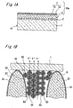
- the electron source 10 includes an electron source element 10a formed on the side of one surface of an insulative substrate 1 (e.g. a glass substrate having an insulation performance or a ceramic substrate having an insulation performance).
- the electron source element 10a includes a lower electrode 2 formed on the side of the above surface of the insulative substrate 1, a composite nanocrystal layer 6 formed on the lower electrode 2, and a surface electrode 7 formed on the composite nanocrystal layer 6.
- the composite nanocrystal layer 6 includes a polycrystalline silicon, and a number of nanocrystalline silicons residing around the grain boundary of the polycrystalline silicon.
- the surface electrode 7 is opposed to the lower electrode 2, and the composite nanocrystal layer is sandwiched between the surface electrode 7 and the lower electrode 2.
- the thickness of the lower electrode 2 is set at about 300 nm (e.g. 330 nm), and the thickness of the surface electrode 7 is set at about 10 nm.
- the lower electrode 2 is formed of a single-layer or multilayer metal thin film made of metal material (e.g. elemental metal such as Cr, W, Ti, Ta, Ni, Al, Cu, Au, Pt or Mo; alloy thereof; or intermetallic compound such as silicide).
- the composite nanocrystal layer 6 is formed by subjecting a polycrystalline silicon to a nanocrystallization process and an oxidation process.
- the composite nanocrystal layer 6 includes a plurality of polycrystalline silicon grains 51, a thin silicon oxide film 52 formed over the surface of each of the grains 51, the number of nanocrystalline silicons 63 residing between the adjacent grains 51, and a silicon oxide film 64 formed over the surface of each of the nanocrystalline silicons 63.
- the silicon oxide film 64 is an insulating film having a thickness less than the crystal grain size of the nanocrystalline silicon 63. It is believed that the remaining region of the composite nanocrystal layer 6 other than the grains 51, the nanocrystalline silicons 63 and the silicon oxide films 52, 64 is an amorphous region 65 of amorphous silicon or partially oxidized amorphous silicon.
- the composite nanocrystal layer 6 includes the polycrystalline silicon, and the number of nanocrystalline silicons 63 residing around the grain boundary of the polycrystalline silicon.
- Each of the grains 51 extends in the thickness direction of the lower electrode 2.
- a plurality of composite nanocrystal layers 6 serve as a drift layer (strong electric field drift layer).
- the surface electrode 7 is formed of a carbon thin film 7a deposited (laminated) on the composite nanocrystal layer 6, and a metal thin film 7b deposited on the carbon thin film 7a.
- the carbon thin film 7a is in contact with the nanocrystalline silicons 63 through the respective silicon oxide films 64 formed over the surface of the nanocrystalline silicons 63.
- the state where the carbon thin film 7a is in indirect contact with the nanocrystalline silicons 63 through the silicon oxide films 64 is also described herein by using the expression "the carbon thin film 7a is in contact with the nanocrystalline silicons 63".
- the thickness of the carbon thin film 7a in the surface electrode 7 is set in the range of 1 nm to 5 nm. Further, the total thickness of the carbon thin film 7a and the metal thin film 7b is arranged at about 10 nm.
- the carbon thin film 7a is made of carbon belonging to Group IV elements as with silicon which is a primary component of the composite nanocrystal layer 6 serving as a base thereof, it has excellent compatibility with the composite nanocrystal layer 6, and high water-repellency.
- the carbon thin film 7a can also provide excellent coverage while facilitating reduction in film thickness, and prevent impurities such as oxygen or water from being mixed into the composite nanocrystal layer 6.
- the carbon thin film 7a has excellent adhesion with the composite nanocrystal layer 6 as well as excellent heat resistance and oxidation resistance.
- the carbon thin film 7a may be formed of various types of carbon material such as amorphous carbon, graphite, graphite-like carbon, diamond or diamond-like carbon. If graphite or graphite-like carbon is used, the electrical resistance of the carbon thin film 7a will be reduced as compared to the carbon thin film made of amorphous carbon, diamond or diamond-like carbon. Thus, a required driving voltage and power consumption can be reduced while suppressing undesirable affects from heat generation or voltage drop in the carbon thin film 7a. Further, if an impurity is doped into the carbon thin film 7a to provide a conducting property therein, the electrical resistance of the carbon thin film 7a will be reduced as compared to a non-doped carbon thin film. Thus, a required driving voltage and power consumption can be reduced while suppressing undesirable affects from heat generation or voltage drop in the carbon thin film 7a.
- the metal thin film 7b is made of a material having relatively high conductivity, relatively low work function, excellent oxidation resistance and chemical stability.
- a material includes gold, platinum, silver, copper, hafnium, zirconium, titanium, tantalum, iridium, niobium, chromium, aluminum, and tungsten. Carbide or nitride of these metals may also be used.
- the metal thin film 7a made of these materials can have enhanced adhesion with the carbon thin film 7a to provide an improved yield ratio in the production process of the electron source.
- a collector electrode 9 is disposed in opposed relation to the surface electrode 7. Then, the space between the surface electrode 7 and the collector electrode 9 is maintained in vacuum, and a DC voltage Vps is applied between the surface 'electrode 7 and the lower electrode 2 in such a manner that the surface electrode 7 has a higher potential than that of the lower electrode 2. Further, a DC voltage Vc is applied between the collector electrode 9 and the surface electrode 7 in such a manner that the collector electrode 9 has a higher potential than that of the surface electrode 7.
- the DC voltages Vps, Vc can be adequately set to allow electrons injected into the lower electrode 2 to be emitted through the surface electrode 7 after drifting in the composite nanocrystal layer 6 (one-dot chain lines in FIG. 2 indicate the flow of electrons e - emitted through the surface electrode 7). It is believed that the electrons reaching the surface of the composite nanocrystal layer 6 are hot electrons, and such electrons are emitted to the vacuum space after readily tunneling through the surface electrode 7. In short, an electric field acting on the composite nanocrystal layer 6 when the surface electrode 7 has a higher potential than that of the lower electrode 2 allows electrons to drift from the lower electrode 2 toward the surface electrode 7.
- a current flowing between the surface electrode 7 and the lower electrode 2 is referred to as "diode current Ips", and a current flowing between the collector electrode 9 and the surface electrode 7 is referred to as “emission current (emission electron current) Ie” (see FIG. 2).
- the DC voltage Vps to be applied between the surface electrode 7 and the lower electrode 2 is in a low range of about 10 to 20 V, the electron source 10 according to the present invention can emit electrons.
- the vacuum dependence of electron emission characteristics can be reduced so as to allow electrons to be stably emitted without occurrence of a so-called popping phenomenon.
- the DC voltage Vc is applied between the collector electrode 9 and the surface electrode 7 in such a manner that the collector electrode 9 has a higher potential than that of the surface electrode 7 while applying the DC voltage Vps between the surface electrode 7 and the lower electrode 2 in such a manner that the surface electrode 7 has a higher potential than that of the lower electrode 2.
- Electrons e - are thermally excited, and injected from the lower electrode 2 into the composite nanocrystal layer 6.
- the DC voltage Vps When the DC voltage Vps is applied to the composite nanocrystal layer 6, most of the generated electric field acts on the silicon oxide films 64.
- the electrons e - injected into the composite nanocrystal layer 6 is accelerated by the strong electric field acting on the silicon oxide films 64 to drift in the region of the composite nanocrystal layer 6 between the grains toward the surface electrode 7 in the direction of the arrows at the center of FIG. 1B.
- the DC voltage Vps goes up to a predetermined value (e.g.
- the electrons e - tunneling through the surface electrode 7 are emitted to the vacuum space.
- the electrons e - accelerated by the strong electric field acting on the thin silicon oxide films 64 formed over the respective nanocrystalline silicons are emitted through the surface electrode 7 after drifting in the composite nanocrystal layer 6 without scattering.
- the electrons can be stably emitted from the composite nanocrystal layer 6 without occurrence of the popping phenomenon during the electron emission operation.
- the electrons reaching the surface of the composite nanocrystal layer 6 are emitted to the vacuum space after readily tunneling through the surface electrode 7 because they would be hot electrons as mentioned above.
- the electron source element 10a operable based on the above principle is generally referred to as "Ballistic electron Surface-emitting Device”.
- the surface electrode 7 is formed of the carbon thin film 7a having excellent compatibility with the composite nanocrystal layer 6 serving as a base thereof and high water-repellency, and the metal thin film 7b.
- the carbon thin film 7a can provide excellent coverage while facilitating reduction in film thickness, and prevent impurities such as oxygen or water from being mixed into the composite nanocrystal layer 6.
- the carbon thin film 7a has excellent adhesion with the composite nanocrystal layer 6 as well as excellent heat resistance and oxidation resistance.
- the electron source 10 can prevent or suppress the conventional problems such as the peeling of the surface electrode 7 from the composite nanocrystal layer 6, the aggregation of the components of the surface electrode 7 and the oxidation of the surface electrode 7. Therefore, as compared to the conventional electron source having the surface electrode formed of only the metal electrode, the electron source 10 according to the first embodiment can have enhanced durability while suppressing deterioration in electron emission efficiency.
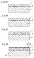
- a production method of the electron source 10 will be described below.
- a lower electrode 2 in the form of a laminate film formed by depositing (laminating) first and second metal layers deposited to have a given thickness for example, a laminate film formed by depositing first and second metal layers to have a thickness of 330 nm, wherein the first metal layer is made of titanium to have a thickness of 80 nm, and the second metal layer is made of tungsten to have a thickness of 250 nm
- a non-doped polycrystalline silicon layer 3 having a given thickness (e.g.
- the lower electrode 2 may be formed, for example, through a sputtering method or a vapor deposition method.
- the polycrystalline silicon layer 3 may be formed, for example, through a CVD method (LPCVD method, plasma CVD method, catalytic-CVD method etc.), a sputtering method, a CGS (Continuous Grain Silicon) method, or a method of depositing amorphous silicon and then laser-annealing the amorphous silicon.
- a composite nanocrystal layer 4 including polycrystalline silicon grains 51, nanocrystalline silicons 63 and amorphous silicon is formed through a nanocrystallization process to provide a structure as shown in FIG. 3B.
- the nanocrystallization process is performed by using a processing bath containing an electrolytic solution which is a mixture prepared by mixing a water solution containing 55 wt% of hydrogen fluoride with ethanol at a ratio of about 1 : 1.
- an electrolytic solution which is a mixture prepared by mixing a water solution containing 55 wt% of hydrogen fluoride with ethanol at a ratio of about 1 : 1.
- a given voltage is applied between a platinum electrode (not shown) and the lower electrode 2.
- the composite nanocrystal layer 4 is formed by supplying a given constant current to the polycrystalline silicon layer 3 while irradiating it with light.
- a composite nanocrystal layer 6 having the structure as shown in FIG. 1B is obtained through an oxidation process to provide a structure as shown in FIG. 3C.
- the oxidation process is performed by using an oxidation-processing bath containing an electrolytic solution (e.g. 1 mol/l of H 2 SO 4 , 1 mol/l of HNO 3 , aqua regia etc.).
- an electrolytic solution e.g. 1 mol/l of H 2 SO 4 , 1 mol/l of HNO 3 , aqua regia etc.
- a given voltage is applied between a platinum electrode (not shown) and the lower electrode 2 to electrochemically oxidize the composite nanocrystal layer 4.
- the composite nanocrystal layer 6 including the grains 51, the nanocrystalline silicons 63, and the silicon oxide films 52, 62 is formed.
- the oxidation process is not limited to the electrochemical oxidation process, but any other suitable oxidation process such as a rapid-heating oxidation process may be used
- a carbon thin film 7a and a metal thin film 7b are formed in turn, and a surface electrode 7 in the form of a laminate film formed by depositing (laminating) the carbon thin film 7a and the metal thin film 7b is formed on the composite nanocrystal layer 6 to provide an electron source 10 having a structure as shown in FIG. 3D.
- the carbon thin film 7a may be formed through various thin-film forming methods, such as a vapor deposition method, a sputtering method, an ion plating method, a thermal CVD method or a PECVD method, it is understood that a thin-film forming method capable of forming a thin film having even film thickness and excellent coverage should be used.
- the metal thin film may be formed through various thin-film forming methods, such as a vapor deposition method, a sputtering method, an ion plating method or a CVD method.
- the above electron-source production method allows an electron source 10 to be produced at a high yield rate while suppressing deterioration in electron emission efficiency and improving durability.
- the composite nanocrystal layer 6 includes the silicon oxide films 52, 64 in addition to the polycrystalline silicon grains 51 and the nanocrystalline silicons 63.
- a silicon nitride film or silicon oxynitride film may be included as a substitute for the silicon oxide films 52, 64.
- a nitriding process or an oxynitriding process may be used instead of the oxidation process.
- the electron source 10 according the first embodiment is used as an electron source for displays, a number of electron source elements 10a may be prepared by appropriately patterning the lower electrode 2, the surface electrode 7 and the composite nanocrystal layer 6, and then arranged on the side of one surface of the insulative substrate 1 in a matrix pattern.
- the surface electrode 7 is composed of the laminate film consisting of the carbon thin film 7a and the metal thin film 7b.
- the surface electrode 7 may be formed of only the carbon thin film 7a.
- An electron source 10 as a first example was produced in accordance with the production method according to the first embodiment, and respective aging characteristic of diode current Ips and emission current Ie in the electron source 10 were measured.
- the measurement result is shown in FIG. 4.
- an insulative substrate 1 is a glass substrate.
- a lower electrode 2 is a laminate film consisting of a titanium layer having a thickness of 80 nm and a tungsten layer having a thickness of 250 nm, which were formed through a sputtering method.
- a non-doped polycrystalline silicon layer 3 (see FIG. 3A) was formed through a plasma CVD method to have a thickness of 1. 5 ⁇ m.
- the nanocrystallization process was performed by using an electrolytic solution prepared by mixing a water solution containing 55 wt% of hydrogen fluoride with ethanol at a ratio of about 1 : 1.
- a constant current of 25 mA/cm 2 from a power supply was supplied between the lower electrode 2 serving as an anode and a platinum electrode serving as a cathode for 8 seconds while irradiating the principal surface of the polycrystalline silicon layer 3 with light by using a 500 W tungsten lump as a light source.
- An electrochemical oxidation process was used as the oxidation process.
- a voltage of 27 V was applied between a platinum electrode (not shown) and the lower electrode 2.
- a surface electrode 7 is a laminate film consisting of a carbon thin film 7a having a thickness of 2 nm and a gold thin film having a thickness of 10 nm which were formed through a sputtering method.
- the electron source 10 was first introduced in a vacuum chamber (not shown), and a collector electrode 9 was disposed in opposed relation to the surface electrode 7 (see FIG. 2). Then, a DC voltage Vc was applied in such a manner that the collector electrode 9 has a higher potential than that of the surface electrode 7 while applying a DC voltage Vps in such a manner that the surface electrode 7 has a higher potential than that of the lower electrode 2.
- FIG. 4 shows the measurement result of electron emission characteristics on the condition that a vacuum in the vacuum chamber is 1 ⁇ 10 -3 Pa, and the DC current Vps is 19 V.
- the horizontal axis represents a lapsed time
- the vertical axis represents a current density.
- ⁇ indicates an aging characteristic of the current density of diode current Ips
- ⁇ indicates an aging characteristic of the current density of emission current Ie.
- the electron source 10 of the first example exhibited an excellent aging characteristic in both the diode current Ips and the emission current Ie.
- FIG. 5 shows respective aging characteristics of diode current Ips and emission current Ie in an emission source 10 of a second example and an electron source of a comparative example.
- the horizontal axis represents a lapsed time
- the vertical axis on the left side representing a current density of diode current Ips
- the vertical axis on the right side representing a current density of emission current Ie.
- ⁇ indicates an aging characteristic of the current density of diode current Ips in the electron source 10 of the second example
- ⁇ indicates an aging characteristic of the current density of emission current Ie in the electron source 10 of the second example
- y indicating an aging characteristic of the current density of diode current Ips in the electron source of the comparative example
- ⁇ indicating an aging characteristic of the current density of emission current Ie in the electron source of the comparative example.
- a voltage of 32 V was applied in the oxidation process.
- the electron source of comparative example has a surface electrode formed of a gold thin film.
- the electron source 10 of the second example using the surface electrode 7 formed of the laminate film consisting of the carbon thin film 7a and the metal thin film 7b exhibited an excellent aging characteristic of the emission current Ie, as compared to the comparative example having the surface electrode formed of only the metal thin film. That is, it is proved that the electron source 10 of the second example provides enhanced aging characteristics in the emission current Ie and the electron emission efficiency, as compared to the comparative example.
- FIG. 6 shows respective aging characteristics of diode current Ips and emission current Ie in an electron source 10 which is different from the electron source concerning FIG. 4 in terms of the conditions of the nanocrystallization process and the oxidation process.
- a cycle consisting of a low current period for supplying a current of 2.5 mA/cm 2 for 2 seconds and a high current period for supplying a current of 25 mA/cm 2 for 4 seconds was repeated three times. Further, a rapid-heating oxidation process was used as the oxidation process.
- the electron source 10 concerning FIG. 6 exhibited an excellent stability against aging as with the electron source of the first example in FIG. 4.
- the thickness of the carbon thin film 7a is set at 1 nm or more, and thus the carbon thin film can be stably introduced.
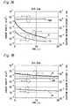
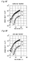
- FIGS. 7A and 7B show the stability of electron emission characteristics or the stability of diode current Ips, emission current Ie and electron emission efficiency of the electron source 10, wherein FIG. 7A shows the characteristics in an electron sources including a carbon thin film 7a having a thickness of 0.5 nm, and FIG. 7B shows the characteristics in an electron sources including a carbon thin film 7a having a thickness of 1.0 nm. As seen in FIG. 7A and 7B, while the carbon thin film 7a having a thickness of 1 nm provides a stable electron emission characteristic, the electron emission characteristic is significantly deteriorated in the carbon thin film 7a having a thickness of 0.5 nm.
- the electron source element can have enhanced characteristics or stability.
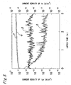
- FIG. 8 shows the relationship between desorbed water content and temperature when the temperature of a silicon layer is increased to desorb water in the silicon layer (through Thermal Desorption Spectrometroy).
- the amount of desorbed water is represented by the value of ion current in proportion thereto.
- some peaks of desorbed water amount can be found in the temperature range of 250°C or less. At these peaks, water absorbed in the silicon layer is desorbed.
- the composite nanocrystal layer 6 (silicon layer) can be heated at 250°C in vacuum before the formation of the carbon thin film 7a, to remove water absorbed in the composite nanocrystal layer 6 so as to provide enhanced characteristics or stability of the electron source element.
- the carbon thin film 7a can be formed in succession to the completion of the removal of the water in the composite nanocrystal layer 6 by heating or warming, to keep the composite nanocrystal layer 6 from water while preventing water from being re-absorbed therein when the quantum device is taken out into atmosphere after the formation of the carbon thin film 7a (capping effect), so as to provide more enhanced characteristics or stability of the electron source element 10a. While the above effect may also be obtained by removing the water through a heat treatment in a process precedent to the formation of the carbon thin film, the composite nanocrystal layer (silicon layer) including the number of nanocrystalline silicons would easily re-absorb water when an electron-source intermediate product is taken out into atmosphere after the heat treatment, due to its high ability of absorbing water therein.
- the formation of the carbon thin film 7a under a temperature of 250°C or more allows the carbon thin film to be formed on the composite nanocrystal layer after removing water therefrom, so as to perform an effective water-removing operation.
- This operation is not limited to the electron source 10, but can also be applied to other quantum device such as a light-emitting device.
- the carbon thin film may be formed after heating the composite nanocrystal layer 6 (silicon layer) at 250°C or more to remove water therefrom, and then cooling the substrate down to room temperature.
- the electron source 10 may be subjected to a heat treatment after the carbon thin film 7a and the metal thin film 7b are formed therein and before the electric field is applied to the electron source 10, to provide enhanced stability and heat resistance of the electron source element 10a or the electron source 10.
- FIGS. 9A to 9D show difference in heat resistance between heat-treated and non-heat-treated electron sources.
- FIG. 9A shows electron emission characteristics measured under the condition that an electric field is applied to the electron source 10 after the formation of the electron source element 10a.
- FIG. 9B shows electron emission characteristics re-measured after the electron source 10 which has been applied with the electric field is subjected to a heat treatment under N 2 atmosphere at 400°C just for 1 hour. As seen in FIGS. 9A and 9B, the deterioration of the emission current Ie shows that the electron source is damaged.
- FIG. 9C shows electron emission characteristics measured under the condition that the electron source 10 is subjected to a heat treatment under N 2 atmosphere at 400°C just for 1 hour after the electron source element 10a is formed and before an electric field is applied to the electron source 10, and then an electric field is applied to the electron source 10.
- the characteristics in FIG. 9C are approximately the same as those in FIG. 9A.
- FIG. 9D shows electron emission characteristics measured under the condition that the electron source 10 subjected to the heat treatment in FIG. 9C is re-subjected to a heat treatment under N 2 atmosphere at 400°C just for 1 hour, and then an electric field is applied to the electron source 10.
- the characteristics in FIG. 9D are approximately the same as those in FIG. 9C, which shows that the electron source is not damaged. That is, the electron source 10 has a heat resistance against 400°C.
- the electron source 10 should be subjected to heat treatment before applying an electric field to the electron source 10, to provide enhanced film quality of the carbon thin film 7a and improved heat resistance of the electron source 10.
- the electron source 10 may be subjected to a heat treatment after the carbon thin film 7a is formed therein and before the electric field is applied to the electron source 10. In this way, the electron source element 10a or the electron source 10 can have enhanced stability and heat resistance as with the above case. This operation is not limited to the electron source 10, but can also be applied to other quantum device such as a light-emitting device.
- the heat resistance against 400°C is one of critical characteristics for the electron device 10 because it is requited, for example, for a vacuum-sealing process using frit glass.
- the heat treatment should be performed at a temperature close to 400°C. If the temperature is excessively lower than 400°C, the film quality will not be sufficiently improved. If the temperature is excessively higher than 400°C, the carbon thin film 7a or the metal thin film 7b will be damaged. Thus, it is desirable to perform the heat treatment at a temperature of 380 to 420°C.
- the above heat treatment or the formation of the surface electro rode 7 can be performed, for example, by the following process. It is understood that this process is not limited to production of the electron source 10, but can also be applied to production of other quantum device such as a light-emitting device.
- a lower electrode 2 made of metal is first formed on an insulative substrate 1 formed of a glass substrate. Then, a polycrystalline silicon layer 3 is formed on the lower electrode 2, for example, through a plasma CVD. The polycrystalline silicon layer 3 is subjected to a nanocrystallization process based on anodic oxidation, and a composite nanocrystal layer 6 is formed by creating oxide films therein through an electrochemical oxidation process.
- a carbon thin film 7a is formed through a sputtering process.
- an electron-source intermediate product is heated up to 250°C under a vacuum of 1 ⁇ 10 -5 Pa or less to form a carbon thin film 7a having a thickness of 1 nm.
- the vacuum is once reduced due to desorption of water from the composite nanocrystal layer 6 which is heated or warmed. After substantially the entire water in the composite nanocrystal layer 6 is desorbed therefrom, the vacuum returns to the original value before heating. Then, the carbon thin film 7a is formed to have a thickness of 1 nm.
- the temperature is reduced while maintaining the vacuum to form a Cr layer having a thickness of 2 nm and an Au layer having a thickness of 8 nm.
- the electron source 10 is subjected to a heat treatment under N 2 atmosphere at 400°C just 1 hour before an electric field is applied to the electron source 10.
- a quantum device is a light-emitting device adapted to emit light based on electric field applied thereto, as one of electronic devices utilizing nanocrystalline silicons.
- the light-emitting device 20 comprises an n-type silicon substrate 21, and an ohmic electrode 22 formed on the back surface of the n-type silicon substrate 21.
- a luminescent layer 26 having a number of nanocrystalline silicons 63 is formed on the front surface of the silicon substrate 21, and an upper electrode 27 is formed on the luminescent layer 26.
- a lower electrode 25 is comprised of the silicon substrate 21 and the ohmic electrode 22.
- the luminescent layer 26 is sandwiched between the lower electrode 25 and the upper electrode 27.
- the lower electrode 25 is disposed on one side in the thickness direction of the luminescent layer 26, and the upper electrode 27 is disposed on the other side, so that the lower electrode 25 and the upper electrode 27 act as a pair of electrodes.
- light generated in the luminescent layer 26 is output outside through the upper electrode 27.
- the thickness of the upper electrode 27 is set at about 10 nm.
- the luminescent layer 26 is formed by subjecting a polycrystalline silicon layer or a silicon layer to a nanocrystallization process and an oxidation process.
- the luminescent layer 26 includes a plurality of polycrystalline silicon grains 51, a thin silicon oxide film 52 formed over the surface of each of the grains 51, the number of nanocrystalline silicons 63 residing between the adjacent grains 51, and a silicon oxide film 64 formed over the surface of each of the nanocrystalline silicons 63.
- the silicon oxide film 64 is an insulating film having a thickness less than the crystal grain size of the nanocrystalline silicon 63. It is believed that the remaining region of the luminescent layer 26 other than the grains 51, the nanocrystalline silicons 63 and the silicon oxide films 52, 64 is formed.of amorphous silicon or partially oxidized amorphous silicon. That is, the luminescent layer 26 includes the polycrystalline silicon, and the number of nanocrystalline silicons 63 residing around the grain boundary of the polycrystalline silicon. Each of the grains 51 extends in the thickness direction of the silicon substrate 21.
- the upper electrode 27 is formed of a carbon thin film 27a laminated on the luminescent layer 26, and a metal thin film 27b laminated on the carbon thin film 27a.
- the carbon thin film 27a is in contact with the nanocrystalline silicons 63 through the respective silicon oxide films 64 formed over the surface of the nanocrystalline silicons 63.
- the thickness of the carbon thin film 27a in the upper electrode 27 is set in the range of 1 nm to 5 nm. Further, the total thickness of the carbon thin film 27a and the metal thin film 27b is arranged at about 10 nm.
- the carbon thin film 27a has excellent compatibility with the luminescent layer 26, and high water-repellency.
- the carbon thin film 27a can also provide excellent coverage while facilitating reduction in film thickness, and prevent impurities such as oxygen or water from being mixed into the luminescent layer 26.
- the carbon thin film 27a has excellent adhesion with the luminescent layer 26 as well as excellent heat resistance and oxidation resistance.
- the material of the carbon thin film 27a may be selected on the same basis as that of the carbon thin film 7a in the first embodiment. In this case, it is understood that the same effects as those in the first embodiment can be obtained. Further, if an impurity is doped into the carbon thin film 27a to provide a conducting property therein, the electrical resistance of the carbon thin film 27a will be reduced. Thus, a required driving voltage and power consumption can be reduced while suppressing undesirable affects from heat generation or voltage drop in the carbon thin film 27a, as with the carbon thin film 7a in the first embodiment.
- the material of the metal thin film 27b may be selected on the same basis as that of the metal thin film 7b in the first embodiment. In this case, it is understood that the same effects as those in the first embodiment can be obtained.
- a voltage may be applied between the upper electrode 27 and the lower electrode 25.
- the luminescent layer 26 generates light in response to an electric field acting thereon when the voltage is applied between the upper electrode 27 and the lower electrode 25. The light generated in the luminescent layer 26 is emitted outside after transmitting through the upper electrode 27.
- the upper electrode 27 is formed of the carbon thin film 27a having excellent compatibility with the luminescent layer 26 serving as a base thereof and high water-repellency, and the metal thin film 27b.
- the carbon thin film 27a can provide excellent coverage while facilitating reduction in film thickness, and prevent impurities such as oxygen or water from being mixed into the luminescent layer 26.
- the carbon thin film 27a has excellent adhesion with the luminescent layer 26 as well as excellent heat resistance and oxidation resistance.
- the light-emitting device 20 can prevent or suppress the conventional problems such as the peeling of the upper electrode 27 from the luminescent layer 26, the aggregation of the components of the upper electrode 27 and the oxidation of the upper electrode 27. Therefore, as compared to the conventional light-emitting device having the upper electrode formed of only the metal electrode, the light-emitting device 20 according to the second embodiment can have enhanced durability while suppressing deterioration in optical output.
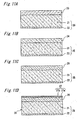
- an ohmic electrode 22 is first formed on the back surface of a silicon substrate 21. Then, a non-doped polycrystalline silicon layer 23 having a given thickness (e.g. 1.5 ⁇ m) is formed on the principal surface of the silicon substrate 21 to provide a structure as shown in FIG. 11A.
- the non-doped polycrystalline silicon layer 23 may be formed through the same method as that of the polycrystal silicon layer 3 in the first embodiment.
- a nanocrystal layer 24 including a polycrystalline silicon, nanocrystalline silicons and amorphous silicons is formed through a nanocrystallization process to provide a structure as shown in FIG. 11B.
- the nanocrystallization process may be the same as that in the first embodiment.
- a luminescent layer 26 having the structure as shown in FIG. 10B is obtained through an oxidation process to provide a structure as shown in FIG. 11C.
- the oxidation process may be the same as that in the first embodiment.
- a carbon thin film 27a and a metal thin film 27b are formed in turn.
- an upper electrode 27 in the form of a laminate film formed of the carbon thin film 27a and the metal thin film 27b is formed on the luminescent layer 26 to provide a light-emitting device 20 having a structure as shown in FIG. 11D.
- the respective methods of forming the carbon thin film 27a and the metal thin film 27b may be the same as those of forming the carbon thin film 7a and the metal thin film 7b in the first embodiment, respectively.
- the above production method allows a light-emitting device 20 to be produced at a high yield rate while suppressing deterioration in optical output and improving durability.
- the luminescent layer 26 includes the silicon oxide films 52, 64 in addition to the polycrystalline silicon grains 51 and the nanocrystalline silicons 63.
- a silicon nitride film or silicon oxynitride film may be included as a substitute for the silicon oxide films 52, 64.
- a nitriding process or an oxynitriding process may be used instead of the oxidation process.
- the upper electrode 27 is composed of the laminate film consisting of the carbon thin film 27a and the metal thin film 27b.
- the supper electrode 27 may be formed of only the carbon thin film 27a.
- the lower electrode 25 is composed of the silicon substrate 21 and the ohmic electrode 22.
- the lower electrode may be a single-layer or multilayer metal thin film made of metal and formed on the insulative substrate, as in the first embodiment.
- the grains 51 are not essentially included therein.
- a part of the principle surface of the silicon substrate 21 may be subjected to the nanocrystallization process and the oxidation process without forming the polycrystalline silicon layer 23 on the principal surface of the silicon substrate 21.
- the silicon oxide films 52, 62 may be not essentially included. In this case, the oxidation process may be omitted, or the silicon oxide films 52, 62 may be removed after the formation of the silicon oxide films 52, 62.
- the non-doped polycrystalline silicon layer 23 is formed on the n-type silicon substrate 21.
- an n-type polycrystalline silicon layer may be used as the polycrystalline silicon layer 23.
- a p-type silicon substrate and a p-type polycrystalline silicon layer may be used as the silicon substrate 21 and the polycrystalline silicon layer 23, respectively.
- a light-emitting device 20 as one example was actually produced in accordance with the production method according to the second embodiment, and a voltage-current characteristic and electroluminescence intensity (EL intensity) were measured.
- the measurement result is shown in FIG. 12.
- an n-type silicon substrate having a resistivity of 0.1 ⁇ cm was used as the silicon substrate 21.
- a non-doped polycrystalline silicon layer 23 (see FIG. 11A) was formed through a plasma CVD method to have a thickness of 1. 5 ⁇ m.
- the nanocrystallization process was performed by using an electrolytic solution prepared by mixing a water solution containing 55 wt% of hydrogen fluoride with ethanol at a ratio of about 1 : 1.
- a constant current of 25 mA/cm 2 from a power supply was supplied between the lower electrode 25 serving as an anode and a platinum electrode serving as a cathode for 8 seconds while irradiating the principal surface of the polycrystalline silicon layer 23 with light by using a 500 W tungsten lump as a light source.
- An electrochemical oxidation process was used as the oxidation process.
- a voltage of 27 V was applied between a platinum electrode (not shown) and the lower electrode 25.
- An upper electrode 27 is a laminate film consisting of a carbon thin film 27a having a thickness of 2 nm and a gold thin film having a thickness of 10 nm which were formed through a sputtering method.
- the horizontal axis represents a voltage applied between the upper electrode 27 and the lower electrode 25, and the vertical axis on the left side representing a current density of a current flowing between the upper electrode 27 and the lower electrode 25, and the vertical axis on the right side representing an electroluminescence intensity.
- a indicates a dependence of the current density of the current flowing between the electrodes 27, 25 to the applied voltage
- ⁇ indicates a dependence of the electroluminescence intensity to the applied voltage.
- the light-emitting device 20 of this example provided excellent optical output, irrespective of the polarity of the voltage applied between the upper electrode 27 and the lower electrode 25.
- FIG. 13 shows a graph showing respective aging characteristics of the current density of the current flowing between the electrodes 27, 25, and the electroluminescence intensity.
- the horizontal axis represents a lapsed time
- the vertical axis on the left side representing the current density of the current flowing between the upper electrode 27 and the lower electrode 25, and the vertical axis on the right side representing the electroluminescence intensity.
- ⁇ indicates an aging characteristic of the current density of the current flowing between the upper electrode 27 and the lower electrode 25, and ⁇ indicates an aging characteristic of the electroluminescence intensity.
- the light-emitting device 20 of this example provided excellent aging characteristics. While not shown in FIG. 13, the light-emitting device 20 of this example also has excellent aging characteristics in both the current density and the electroluminescence intensity, as compared to the conventional light-emitting device having the upper electrode 27 formed of only the metal thin film.
- the quantum device according to the present invention is useful for providing improved adhesion of the surface electrode with the silicon layer, heat resistance and oxidation resistance as well as enhanced durability, and suitable as electron sources or light-emitting devices.
Landscapes
- Engineering & Computer Science (AREA)
- Chemical & Material Sciences (AREA)
- Nanotechnology (AREA)
- Physics & Mathematics (AREA)
- Crystallography & Structural Chemistry (AREA)
- Biophysics (AREA)
- Manufacturing & Machinery (AREA)
- Life Sciences & Earth Sciences (AREA)
- Organic Chemistry (AREA)
- Optics & Photonics (AREA)
- Materials Engineering (AREA)
- Inorganic Chemistry (AREA)
- Mathematical Physics (AREA)
- Theoretical Computer Science (AREA)
- Cold Cathode And The Manufacture (AREA)
- Cathode-Ray Tubes And Fluorescent Screens For Display (AREA)
- Physical Deposition Of Substances That Are Components Of Semiconductor Devices (AREA)
Abstract
Description
Claims (15)
- A quantum device comprising:a lower electrode;a silicon layer formed on said lower electrode, said silicon layer including a number of nanocrystalline silicons to induce a quantum effect in response to an electric field applied thereto; anda carbon thin film formed on said silicon layer to be in contact with the nanocrystalline silicons.
- The quantum device according to claim 1, further comprising a metal thin film formed on said carbon thin film.
- The quantum device according to claim 2, wherein said metal thin film is composed of a material selected from the group consisting of gold, platinum, silver, copper, hafnium, zirconium, titanium, tantalum, iridium, niobium, chromium, aluminum, and carbide or nitride thereof.
- The quantum device according to claim 1, wherein said carbon thin film is composed of graphite or graphite-like carbon.
- The quantum device according to claim 1, wherein said carbon thin film has a conducting property yielded by doping an impurity therein.
- The quantum device according to claim 1, wherein said carbon thin film has a thickness of 5 nm or less.
- The quantum device according to claim 6, wherein the thickness of said carbon thin film is 1 nm or more.
- The quantum device according to claim 1, wherein said carbon thin film is a film formed under a temperature of 250°C or more.
- The quantum device according to claim 1, which is subjected to a heat treatment after said carbon thin film is formed therein and before the electric field is applied thereto.
- The quantum device according to claim 2, which is subjected to a heat treatment after said carbon thin film and said metal thin film are formed therein and before the electric field is applied thereto.
- The quantum device according to claim 9, wherein said heat treatment is performed at a temperature of 380 to 420°C.
- The quantum device according to claim 10, wherein said heat treatment is performed at a temperature of 380 to 420°C.
- The quantum device according to any one of claims 1 to 12, wherein said silicon layer is a strong electric field drift layer capable of accelerating electrons based on a strong electric field effect, wherein said quantum device serves as an electron source.
- The quantum device according to claim 13, wherein said silicon layer is a composite nanocrystal layer which includes a polycrystalline silicon, and a number of nanocrystalline silicons residing around the grain boundary of said polycrystalline silicon.
- The quantum device according to any one of claims 1 to 12, wherein said silicon layer is a luminescent layer capable of generating light in response to an electric field applied thereto, wherein said quantum device serves as a light-emitting device.
Applications Claiming Priority (3)
| Application Number | Priority Date | Filing Date | Title |
|---|---|---|---|
| JP2002064287 | 2002-03-08 | ||
| JP2002064287 | 2002-03-08 | ||
| PCT/JP2003/002688 WO2003077320A1 (en) | 2002-03-08 | 2003-03-07 | Quantum device |
Publications (2)
| Publication Number | Publication Date |
|---|---|
| EP1484800A1 true EP1484800A1 (en) | 2004-12-08 |
| EP1484800A4 EP1484800A4 (en) | 2008-10-29 |
Family
ID=27800212
Family Applications (1)
| Application Number | Title | Priority Date | Filing Date |
|---|---|---|---|
| EP03744009A Ceased EP1484800A4 (en) | 2002-03-08 | 2003-03-07 | QUANTUM DEVICE |
Country Status (7)
| Country | Link |
|---|---|
| US (1) | US6940087B2 (en) |
| EP (1) | EP1484800A4 (en) |
| JP (1) | JP4285684B2 (en) |
| KR (1) | KR100625836B1 (en) |
| CN (1) | CN100376040C (en) |
| TW (1) | TW588389B (en) |
| WO (1) | WO2003077320A1 (en) |
Families Citing this family (24)
| Publication number | Priority date | Publication date | Assignee | Title |
|---|---|---|---|---|
| US20040129223A1 (en) * | 2002-12-24 | 2004-07-08 | Park Jong Hyurk | Apparatus and method for manufacturing silicon nanodot film for light emission |
| JP2005285380A (en) * | 2004-03-26 | 2005-10-13 | Quantum 14:Kk | Diode element and device using the same |
| WO2006011237A1 (en) * | 2004-07-27 | 2006-02-02 | Quantum 14 Kk | Light-emitting element, light-emitting device and information display |
| CN101213638B (en) | 2005-06-30 | 2011-07-06 | L·皮尔·德罗什蒙 | Electronic component and manufacturing method |
| KR100637245B1 (en) * | 2005-08-29 | 2006-10-23 | 삼성에스디아이 주식회사 | DC plasma display panel and manufacturing method thereof |
| US8835941B2 (en) * | 2006-02-09 | 2014-09-16 | Qd Vision, Inc. | Displays including semiconductor nanocrystals and methods of making same |
| WO2007143197A2 (en) | 2006-06-02 | 2007-12-13 | Qd Vision, Inc. | Light-emitting devices and displays with improved performance |
| JP5344205B2 (en) * | 2006-03-22 | 2013-11-20 | Nltテクノロジー株式会社 | Multilayer wiring, semiconductor device using the multilayer wiring, and manufacturing method thereof |
| US7410852B2 (en) | 2006-04-21 | 2008-08-12 | International Business Machines Corporation | Opto-thermal annealing methods for forming metal gate and fully silicided gate field effect transistors |
| JP4757740B2 (en) * | 2006-08-21 | 2011-08-24 | 富士通株式会社 | Semiconductor device |
| WO2008085210A2 (en) | 2006-09-12 | 2008-07-17 | Qd Vision, Inc. | Electroluminescent display useful for displaying a predetermined pattern |
| JP4122043B1 (en) * | 2007-04-25 | 2008-07-23 | 株式会社クレステック | Surface emission type electron source and drawing apparatus |
| US9525148B2 (en) | 2008-04-03 | 2016-12-20 | Qd Vision, Inc. | Device including quantum dots |
| CN102047098B (en) | 2008-04-03 | 2016-05-04 | Qd视光有限公司 | Light emitting device including quantum dots |
| JP5374432B2 (en) | 2010-03-31 | 2013-12-25 | パナソニック株式会社 | Electronic device and manufacturing method thereof |
| JP5783798B2 (en) * | 2010-10-07 | 2015-09-24 | シャープ株式会社 | ELECTRON EMITTING ELEMENT AND DEVICE EQUIPPED WITH THE SAME |
| CN103415925A (en) | 2010-11-03 | 2013-11-27 | L·皮尔·德罗什蒙 | Semiconductor chip carrier with monolithically integrated quantum dot devices and method of manufacturing the same |
| JP5238795B2 (en) | 2010-11-19 | 2013-07-17 | シャープ株式会社 | Electron emitting device and driving method thereof |
| US9490414B2 (en) | 2011-08-31 | 2016-11-08 | L. Pierre de Rochemont | Fully integrated thermoelectric devices and their application to aerospace de-icing systems |
| JP2014056677A (en) * | 2012-09-11 | 2014-03-27 | Panasonic Corp | Manufacturing method of electron source |
| JP6247846B2 (en) * | 2013-07-09 | 2017-12-13 | シャープ株式会社 | Electron emitter |
| JP6221914B2 (en) * | 2014-04-11 | 2017-11-01 | 日本電気硝子株式会社 | Method for manufacturing light emitting device |
| JP6889629B2 (en) * | 2017-07-31 | 2021-06-18 | シャープ株式会社 | Manufacturing method of electron emitting element and electron emitting element |
| CN113130809B (en) * | 2019-12-30 | 2022-06-07 | Tcl科技集团股份有限公司 | Composite electrode and preparation method thereof, and quantum dot light-emitting diode |
Family Cites Families (26)
| Publication number | Priority date | Publication date | Assignee | Title |
|---|---|---|---|---|
| US90211A (en) * | 1869-05-18 | Improved carpet-sweeper | ||
| US13215A (en) * | 1855-07-10 | Straw-cutter | ||
| US17369A (en) * | 1857-05-26 | Wagon-coupling | ||
| US197457A (en) * | 1877-11-27 | Improvement in windmills | ||
| US102793A (en) * | 1870-05-10 | Improvement in bolts for safes | ||
| DE3687529T2 (en) * | 1985-03-20 | 1993-05-13 | Sharp Kk | PRODUCTION OF GRAPHITE STORAGE COMPOUND AND DOPED CARBON FILMS. |
| JPH0690019A (en) | 1992-09-07 | 1994-03-29 | Res Dev Corp Of Japan | Silicon light emitting display device |
| JPH08236799A (en) * | 1995-02-24 | 1996-09-13 | Fuji Electric Co Ltd | Semiconductor radiation detecting element and rectifying element |
| US5990605A (en) | 1997-03-25 | 1999-11-23 | Pioneer Electronic Corporation | Electron emission device and display device using the same |
| TW391022B (en) | 1997-10-29 | 2000-05-21 | Mitsubishi Rayon Co | Field emission electron source, method of producing the same, and use of the same |
| JP2966842B1 (en) * | 1998-09-25 | 1999-10-25 | 松下電工株式会社 | Field emission electron source |
| KR100338140B1 (en) | 1998-09-25 | 2002-05-24 | 이마이 기요스케 | Electric field emission type electron source |
| TW436837B (en) | 1998-11-16 | 2001-05-28 | Matsushita Electric Works Ltd | Field emission-type electron source and manufacturing method thereof and display using the electron source |
| TW472273B (en) | 1999-04-23 | 2002-01-11 | Matsushita Electric Works Ltd | Field emission-type electron source and manufacturing method thereof |
| KR100374782B1 (en) | 1999-10-18 | 2003-03-04 | 마츠시다 덴코 가부시키가이샤 | Field emision-type electron source and manufacturing method thereof |
| US6765342B1 (en) * | 1999-10-18 | 2004-07-20 | Matsushita Electric Work, Ltd. | Field emission-type electron source and manufacturing method thereof |
| JP3789064B2 (en) | 1999-10-27 | 2006-06-21 | パイオニア株式会社 | Electron emitter |
| JP2001143607A (en) | 1999-11-18 | 2001-05-25 | Canon Inc | Electron emitting element, electron source and image forming apparatus |
| JP3874396B2 (en) | 2000-01-13 | 2007-01-31 | パイオニア株式会社 | ELECTRON EMITTING ELEMENT, MANUFACTURING METHOD THEREOF, AND DISPLAY DEVICE USING ELECTRON EMITTING ELEMENT |
| JP4438156B2 (en) | 2000-02-07 | 2010-03-24 | パナソニック電工株式会社 | Memory device and manufacturing method thereof |
| TWI286773B (en) | 2000-10-26 | 2007-09-11 | Matsushita Electric Works Ltd | Field emission type electron source |
| WO2002089166A1 (en) | 2001-04-24 | 2002-11-07 | Matsushita Electric Works, Ltd. | Field emission electron source and production method thereof |
| US6753196B2 (en) | 2001-06-26 | 2004-06-22 | Matsushita Electric Works, Ltd. | Method of and apparatus for manufacturing field emission-type electron source |
| JP2003100201A (en) | 2001-09-25 | 2003-04-04 | Matsushita Electric Works Ltd | Field emission electron source and manufacturing method thereof |
| CN1216394C (en) | 2001-09-25 | 2005-08-24 | 松下电工株式会社 | Field emission type electron source |
| EP1306870B1 (en) | 2001-10-29 | 2010-06-30 | Panasonic Electric Works Co., Ltd. | Field emission-type electron source and method of biasing the same |
-
2003
- 2003-03-07 TW TW092105138A patent/TW588389B/en not_active IP Right Cessation
- 2003-03-07 WO PCT/JP2003/002688 patent/WO2003077320A1/en not_active Ceased
- 2003-03-07 EP EP03744009A patent/EP1484800A4/en not_active Ceased
- 2003-03-07 JP JP2003062141A patent/JP4285684B2/en not_active Expired - Fee Related
- 2003-03-07 CN CNB038006863A patent/CN100376040C/en not_active Expired - Fee Related
- 2003-03-07 KR KR1020047000749A patent/KR100625836B1/en not_active Expired - Fee Related
- 2003-03-07 US US10/480,262 patent/US6940087B2/en not_active Expired - Fee Related
Also Published As
| Publication number | Publication date |
|---|---|
| WO2003077320A1 (en) | 2003-09-18 |
| US20040195575A1 (en) | 2004-10-07 |
| TW200305178A (en) | 2003-10-16 |
| TW588389B (en) | 2004-05-21 |
| KR100625836B1 (en) | 2006-09-20 |
| JP2003338619A (en) | 2003-11-28 |
| CN100376040C (en) | 2008-03-19 |
| US6940087B2 (en) | 2005-09-06 |
| JP4285684B2 (en) | 2009-06-24 |
| EP1484800A4 (en) | 2008-10-29 |
| KR20040020971A (en) | 2004-03-09 |
| CN1533608A (en) | 2004-09-29 |
Similar Documents
| Publication | Publication Date | Title |
|---|---|---|
| US6940087B2 (en) | Quantum device | |
| US20030076023A1 (en) | Field emission-type electron source | |
| US6765342B1 (en) | Field emission-type electron source and manufacturing method thereof | |
| TWI286773B (en) | Field emission type electron source | |
| JP3789064B2 (en) | Electron emitter | |
| HK1069919A (en) | Quantum device | |
| US7268476B2 (en) | Field emission-type electron source and method of producing the same | |
| US8653519B2 (en) | Electronic device and method for manufacturing same | |
| JP4415922B2 (en) | Method for forming silicon oxide film | |
| JP2003187688A (en) | Field emission type electron source and manufacturing method of the same | |
| JP3963121B2 (en) | Anodic oxidation method, electrochemical oxidation method, field emission electron source and method for producing the same | |
| JP4616538B2 (en) | Manufacturing method of field emission electron source | |
| JP2003281992A (en) | Electron source and manufacturing method therefor | |
| JP2003100201A (en) | Field emission electron source and manufacturing method thereof | |
| JP3709842B2 (en) | Field emission electron source and manufacturing method thereof | |
| JP2003281993A (en) | Electron source and manufacturing method therefor | |
| EP1328003B1 (en) | Field emission-type electron source | |
| EP1523025B1 (en) | Field emission-type electron source | |
| JP4433857B2 (en) | Field emission electron source | |
| JP3478206B2 (en) | Method for manufacturing field emission electron source | |
| JP2002134002A (en) | Field emission type electron source and its manufacturing method | |
| JP2003331718A (en) | Manufacturing method of field emission electron source | |
| HK1036685A (en) | Field emission-type electron source and manufacturing method thereof | |
| JP2003331719A (en) | Manufacturing method of field emission electron source | |
| JPH06112154A (en) | Formation of electrode of semiconductor device |
Legal Events
| Date | Code | Title | Description |
|---|---|---|---|
| PUAI | Public reference made under article 153(3) epc to a published international application that has entered the european phase |
Free format text: ORIGINAL CODE: 0009012 |
|
| 17P | Request for examination filed |
Effective date: 20031213 |
|
| AK | Designated contracting states |
Kind code of ref document: A1 Designated state(s): AT BE BG CH CY CZ DE DK EE ES FI FR GB GR HU IE IT LI LU MC NL PT RO SE SI SK TR |
|
| REG | Reference to a national code |
Ref country code: HK Ref legal event code: DE Ref document number: 1069919 Country of ref document: HK |
|
| A4 | Supplementary search report drawn up and despatched |
Effective date: 20080929 |
|
| RAP1 | Party data changed (applicant data changed or rights of an application transferred) |
Owner name: KOSHIDA, NOBUYOSHI Owner name: PANASONIC ELECTRIC WORKS CO., LTD. |
|
| 17Q | First examination report despatched |
Effective date: 20090406 |
|
| APBK | Appeal reference recorded |
Free format text: ORIGINAL CODE: EPIDOSNREFNE |
|
| APBN | Date of receipt of notice of appeal recorded |
Free format text: ORIGINAL CODE: EPIDOSNNOA2E |
|
| APBR | Date of receipt of statement of grounds of appeal recorded |
Free format text: ORIGINAL CODE: EPIDOSNNOA3E |
|
| APAF | Appeal reference modified |
Free format text: ORIGINAL CODE: EPIDOSCREFNE |
|
| RAP1 | Party data changed (applicant data changed or rights of an application transferred) |
Owner name: KOSHIDA, NOBUYOSHI Owner name: PANASONIC CORPORATION |
|
| REG | Reference to a national code |
Ref country code: HK Ref legal event code: WD Ref document number: 1069919 Country of ref document: HK |
|
| APBT | Appeal procedure closed |
Free format text: ORIGINAL CODE: EPIDOSNNOA9E |
|
| REG | Reference to a national code |
Ref country code: DE Ref legal event code: R003 |
|
| STAA | Information on the status of an ep patent application or granted ep patent |
Free format text: STATUS: THE APPLICATION HAS BEEN REFUSED |
|
| 18R | Application refused |
Effective date: 20161011 |