EP1482653A1 - Variable communication system - Google Patents
Variable communication system Download PDFInfo
- Publication number
- EP1482653A1 EP1482653A1 EP03744722A EP03744722A EP1482653A1 EP 1482653 A1 EP1482653 A1 EP 1482653A1 EP 03744722 A EP03744722 A EP 03744722A EP 03744722 A EP03744722 A EP 03744722A EP 1482653 A1 EP1482653 A1 EP 1482653A1
- Authority
- EP
- European Patent Office
- Prior art keywords
- information
- clock
- amount
- spreading
- communication
- Prior art date
- Legal status (The legal status is an assumption and is not a legal conclusion. Google has not performed a legal analysis and makes no representation as to the accuracy of the status listed.)
- Withdrawn
Links
Images


Classifications
-
- H—ELECTRICITY
- H04—ELECTRIC COMMUNICATION TECHNIQUE
- H04B—TRANSMISSION
- H04B1/00—Details of transmission systems, not covered by a single one of groups H04B3/00 - H04B13/00; Details of transmission systems not characterised by the medium used for transmission
- H04B1/69—Spread spectrum techniques
- H04B1/707—Spread spectrum techniques using direct sequence modulation
-
- H—ELECTRICITY
- H04—ELECTRIC COMMUNICATION TECHNIQUE
- H04L—TRANSMISSION OF DIGITAL INFORMATION, e.g. TELEGRAPHIC COMMUNICATION
- H04L25/00—Baseband systems
- H04L25/02—Details ; arrangements for supplying electrical power along data transmission lines
- H04L25/0262—Arrangements for detecting the data rate of an incoming signal
-
- H—ELECTRICITY
- H04—ELECTRIC COMMUNICATION TECHNIQUE
- H04L—TRANSMISSION OF DIGITAL INFORMATION, e.g. TELEGRAPHIC COMMUNICATION
- H04L27/00—Modulated-carrier systems
- H04L27/0008—Modulated-carrier systems arrangements for allowing a transmitter or receiver to use more than one type of modulation
-
- H—ELECTRICITY
- H04—ELECTRIC COMMUNICATION TECHNIQUE
- H04L—TRANSMISSION OF DIGITAL INFORMATION, e.g. TELEGRAPHIC COMMUNICATION
- H04L1/00—Arrangements for detecting or preventing errors in the information received
- H04L1/12—Arrangements for detecting or preventing errors in the information received by using return channel
- H04L1/16—Arrangements for detecting or preventing errors in the information received by using return channel in which the return channel carries supervisory signals, e.g. repetition request signals
- H04L1/18—Automatic repetition systems, e.g. Van Duuren systems
Definitions
- the present invention relates to a digital communication system and, more particularly, to a variable communication system which switches communication schemes in accordance with the communication amount.
- the traffic of communication is detected from an m-sequence signal input to a rate conversion multiplexer (not shown), and the rate conversion multiplexer multiplexes data at a rate corresponding to the traffic.
- a variable rate modulator (not shown) then modulates the multiplexed signal and transmits it to a transmission path at a transmission rate corresponding to the magnitude of the traffic. That is, the modulation clock rate is time-modulated.
- a variable rate demodulator (not shown) performs demodulation, and a rate conversion demultiplexer (not shown) demultiplexes and rate-converts the demodulated signal to reproduce the data.
- Claim 2 in Japanese Patent Laid-Open No. 2000-316035 proposes a technique of efficiently assigning bands by dynamically changing the transmission rate in accordance with the transmission amount as in the above prior art.
- the transmission rate of information to be transmitted is set low to set a line with a low modulation clock rate, whereas as the communication amount increases, a line with a high modulation clock rate and high transmission rate is set.
- a router which has selected a general voice line connects to a predetermined content server on the Internet at a given time point to transfer large-volume data.
- the communication amount increases at this time point. In a case opposite to the above case, the communication amount decreases at a predetermined time point.
- demodulation synchronization when the transmission rates are switched in accordance with the communication amount, demodulation synchronization must be established with respect to the transmission rate after switching at the time of this switching operation. Demodulated data is temporarily interrupted until demodulation synchronization is established. Compare a case wherein the transmission rate after switching is high with a case wherein the transmission rare after switching is low. In the latter case, for example, in a carrier wave reproducing circuit, the frequency error of a reception carrier wave with respect to the modulation clock rate becomes relatively large. For this reason, in a PLL circuit for carrier wave reproduction, it takes a longer time to establish demodulation synchronization than in the case wherein the transmission rate after switching is high.
- a buffer memory In order to prevent omission of information due to the interruption of demodulated data, a buffer memory has been conventionally used. There has been a communication sequence in which when transmission or reception is to be performed, communication data is temporarily stored in the buffer memory, and transmission is stopped at a predetermined timing which poses no problem in the reproduction of information. In this sequence, when the receiving side detects omission of communication data, a re-transmission request is generated to read out the corresponding portion from the buffer memory on the transmitting side and re-transmit it.
- a variable communication system characterized by comprising (I) a transmission device including information amount magnitude discrimination means for discriminating whether an amount of information to be transmitted per unit time is relatively large or small, first communication data sending means for, when the information amount magnitude discrimination means discriminates that the amount of information to be transmitted is relatively large, digitally modulating first information as the information into information in a signal form having a predetermined bandwidth with a predetermined center frequency, and sending out the information as communication data, and second communication data sending means for, when the information amount magnitude discrimination means discriminates that the amount of information to be transmitted is relatively small, digitally modulating second information as the information upon performing spread spectrum to obtain the same bandwidth as the predetermined bandwidth with the center frequency, and sending out the information as the communication data, and (II) a reception device including demodulation means for demodulating the communication data sent from the transmission device, de-spreading appropriateness discrimination means for checking whether or not a signal after demodulation can be normally de-spread,
- the transmission device includes the information amount magnitude discrimination means and discriminates whether the amount of information to be transmitted per unit time is relatively large or small. If it is discriminated from this discrimination result that the information is relatively large, the first communication data sending means digitally modulates the first information into information in a signal form having a predetermined bandwidth with a predetermined center frequency, and sends out the resultant data as communication data. In this regard, there is no specific difference from the prior art. If the information amount magnitude discrimination means discriminates that the information to be transmitted is relatively small, the second information as this information is subjected to spread spectrum and digital modulation to be sent out as communication data. In this case, the necessary bandwidth is spread to the bandwidth associated with the first signal by spread spectrum.
- the center frequency of the second information is also made equal to that of the first information, and the second information is sent out as communication data. This makes it unnecessary for the demodulation means of the reception device to switch frequencies for the first information and the second information. The time required for this operation is also made unnecessary.
- the de-spreading appropriateness discrimination means checks whether or not a signal after demodulation can be normally de-spread. If it is determined that de-spreading can be done, this signal is regarded as the second information and de-spread to be reproduced. If it is determined that de-spreading cannot be done, this signal is regarded as the first information and reproduced without performing any spread spectrum.
- the transmission device may further comprise a transmission buffer which sequentially receives information to be transmitted and outputs the information in synchronism with a predetermined read clock, and the information amount magnitude discrimination means may discriminate from an amount of information left in the transmission buffer whether the amount of information per unit time is relatively large or small.
- the first and second communication data sending means of the transmission device may include chip clock generating means for outputting a chip clock having a predetermined frequency, transmitting-side frequency dividing means for frequency-dividing the chip clock output from the chip clock generating means at a predetermined frequency division ratio, read clock selection means for, when the information amount magnitude discrimination means discriminates that information to be transmitted is relatively large, setting the chip clock as the read clock, and when the information amount magnitude discrimination means discriminates that information to be transmitted is relatively small, setting, as the read clock, a clock obtained by frequency-dividing the chip clock by the transmitting-side frequency dividing means, spreading code generating means for receiving the chip clock and generating a spreading code, transmitting-side switch means which receives an output from the spreading code generating means and is turned on only when the information amount magnitude discrimination means discriminates that information to be transmitted is relatively small, transmitting-side exclusive addition means for calculating exclusive-OR between information output from the transmission buffer in synchronism with the read clock and an output from the transmitting-side switch means, and modulation
- the de-spreading means and the first and second information reproduction means of the reception device may include reception clock generating means for outputting a reception clock identical to the chip clock, de-spreading code generating means for generating a de-spreading code on the basis of the reception clock output from the reception clock generating means, receiving-side switch means which receives an output from the de-spreading code generating means and is turned on only when the de-spreading appropriateness discrimination means discriminates that de-spreading can be performed, receiving-side exclusive addition means for calculating exclusive-OR between an output from the receiving-side switch means and a signal after demodulation by the demodulation means, receiving-side frequency dividing means for frequency-dividing the reception clock at the predetermined frequency division ratio, write clock selection means for, when the de-spreading appropriateness discrimination means discriminates that de-spreading cannot be performed, selecting the reception clock, and when de-spreading appropriateness discrimination means discriminates that de-spreading can be performed, selecting and outputting a clock obtained by frequency
- the transmission device includes the transmission buffer, and the information amount magnitude discrimination means discriminates from the amount of information left in the transmission buffer whether the amount of information input to the device per unit time is relatively large or small.
- the period of a read clock for reading out data from the transmission buffer can be changed in two levels. More specifically, if the information amount magnitude discrimination means discriminates that the information to be transmitted is relatively large, a chip clock is used as a read clock. If the information amount magnitude discrimination means discriminates that the amount of information is relatively small, a slow clock is obtained by frequency-dividing this chip clock using the transmitting-side frequency dividing means. The data read out from the transmission buffer in this manner becomes one input to the transmitting-side exclusive addition means.
- the transmitting-side switch means is a switch which is turned on only when the information amount magnitude discrimination means discriminates that the information to be transmitted is relatively small.
- the modulation means outputs a signal, as communication data, which has a bandwidth corresponding to the information amount. If the information amount magnitude discrimination means determines that the amount of information is relatively small, spread spectrum is performed to spread the bandwidth, and the resultant data is output as communication data, which has the same center frequency as that in the case wherein it is determined that the amount of information is relatively large.
- the demodulation means on the reception device side need not perform demodulation synchronization again. If it is checked on the basis of demodulated data after demodulation by the demodulation means whether spread spectrum can be normally performed, and it is determined that spread spectrum can be performed, the sent signal is regarded as a signal sent by spread spectrum. This signal is then de-spread and written in the reception buffer. Otherwise, the demodulated data after demodulation is written in this reception buffer. In this case, the write clock selection means selects a write clock in accordance with the rate read out from the transmission buffer on the transmission device side. In this manner, the information after demodulation which is to be transmitted is obtained from the reception buffer.
- the first and second communication data sending means of the transmission device may include chip clock generating means for outputting a chip clock having a predetermined frequency, transmitting-side frequency dividing means for frequency-dividing the chip clock output from the chip clock generating means at a predetermined frequency division ratio, read clock selection means for, when the information amount magnitude discrimination means discriminates that information to be transmitted is relatively large, setting the chip clock as the read clock, and when the information amount magnitude discrimination means discriminates that information to be transmitted is relatively small, setting, as the read clock, a clock obtained by frequency-dividing the chip clock by the transmitting-side frequency dividing means, modulation means for digitally modulating information output from the transmission buffer in synchronism with a read clock, spreading code generating means for receiving the chip clock and generating a spreading code, transmitting-side switch means which receives an output from the spreading code generating means and is turned on only when the information amount magnitude discrimination means discriminates that information to be transmitted is relatively small, transmitting-side exclusive addition means for calculating exclusive-OR between an output from the modulation
- reception clock generating means of the reception device may comprise reception clock reproduction means for reproducing a reception clock from communication data input to the demodulation means.
- the information amount magnitude discrimination means of the transmission device may set a predetermined difference between a threshold by which it is discriminated that an information amount is relatively large and a threshold by which it is discriminated that an information amount is relatively small. More specifically, the information amount magnitude discrimination means may set a threshold by which it is discriminated that an information amount is relatively large to a value larger than a threshold by which it is discriminated that an information amount is relatively small.
- the information amount magnitude discrimination means of the transmission device may discriminate, depending on whether or not a path through which information to be transmitted is acquired is a pre-specified path, whether the amount of information to be transmitted per unit time is relatively large or small.
- the information amount magnitude discrimination means may discriminate, depending on whether or not a device which processes information to be transmitted is set in a pre-specified mode, whether the amount of information to be transmitted per unit time is relatively large or small.
- the transmission device and the reception device may comprise a radio device.
- the transmission device may output transmission power in proportion to a transmission rate.
- the transmission rate is low, since the transmission power is decreased, the transmission power density decreases by an amount corresponding to an increase in occupied bandwidth due to spread spectrum.
- Fig. 1 shows the overall arrangement of a variable communication system according to the first embodiment of the present invention.
- This variable communication system is formed as a communication system in which two LANs (Local Area Networks) including a first LAN 101 and a second LAN 102 are connected to each other.
- a host computer (HOST) 103 and first router (Router) 104 are connected to the first LAN 101.
- a first communication device 106 for performing communication with a radio communication channel 105 is connected to the first router 104.
- a terminal 107 controlled by a host computer (not shown) and a second router 108 are connected to the second LAN 102.
- a second communication device 109 for performing communication with the radio communication channel 105 is connected to the second router 108.
- the first and second communication devices 106 and 109 are designed to monitor communication amounts when they perform communication using the radio communication channel 105.
- Each communication device performs communication upon switching information rates depending on whether the communication amount is relatively large or small. Note, however, that the transfer rate of communication data communicated through the radio communication channel 105 is always kept constant, and when the communication amount is relatively large, a general PSK (Phase Shift Keying) modulation scheme is used to transmit information.
- PSK Phase Shift Keying
- spread-spectrum communication is performed. Since the transfer rate of communication data remains unchanged, even if the communication amount varies, transmission rate resynchronization is not required at the time of switching transmission rates. This eliminates any communication interruption time.
- Fig. 2 shows the arrangement of the transmission unit of the first communication device according to this embodiment.
- the transmission unit of the second communication device 109 shown in Fig. 1 basically has the same arrangement as that of the transmission unit of the first communication device 106. Therefore, a description of the transmission unit of the second communication device 109 will be omitted.
- a transmission unit 121 of the first communication device includes a transmission buffer 123 which receives communication data 122 sent from the first router 104 shown in Fig. 1.
- the transmission buffer 123 is a memory with a relatively small capacity.
- a communication amount monitoring circuit 124 monitors the communication amount by checking a change in the consumption of the buffer. The communication amount monitoring circuit 124 then outputs a communication amount magnitude discrimination signal 125 indicating whether the amount of communication data 122 sent from the first router 104 is relatively large or small.
- the communication amount magnitude discrimination signal 125 is input to a read clock selector 126 and the control terminal of a spreading code selection switch 127.
- the read clock selector 126 selects either a chip clock 129 having a predetermined frequency output from a chip clock oscillator 128 or a frequency division output 132 from a 1/N frequency divider 131 which frequency-divides the chip clock 129 to 1/N, and supplies it as a read clock 133 to the transmission buffer 123.
- the numerical value N is an integer equal to or more than two.
- the spreading code selection switch 127 is a switch for turning on/off the supply of a spreading code 135 output from the spreading code generating circuit 134 to one input terminal of an exclusive adder 136. When the contact of the spreading code selection switch 127 is open, a fixed value of signal "0" or signal "1" is supplied to this input terminal of the exclusive adder 136.
- the chip clock 129 is supplied to the spreading code generating circuit 134.
- Communication data 137 read out from the transmission buffer 123 in accordance with the read clock 133 is input to the other input terminal of the exclusive adder 136.
- the exclusive adder 136 calculates the exclusive-OR (EOR) of the input spreading code 135 and the communication data 137, and inputs an addition output 138 to a modulator 139.
- the modulator 139 modulates this and sends out a modulated output 141 to the radio communication channel 105 shown in Fig. 1. In this case, the modulator 139 performs spread-spectrum modulation when the communication amount is relatively small, and performs general PSK modulation when the communication amount is relatively large.
- Fig. 3 shows the arrangement of the reception unit of the second communication device according to this embodiment.
- the reception unit of the first communication device 106 shown in Fig. 1 basically has the same arrangement as that of the reception unit of the second communication device 109. Therefore, a description of the reception unit of the first communication device 106 will be omitted.
- a reception unit 151 of the second communication device includes a demodulator 153 which receives a reception signal 152 received from the radio communication channel 105 shown in Fig. 1 and demodulates the signal.
- the demodulator 153 outputs demodulated data 154.
- the demodulated data 154 becomes one input to an exclusive adder 155 and also becomes an input to a de-spreading synchronization circuit 156.
- the demodulated data 154 is also input to a reception clock reproducing circuit 158 to reproduce a reception clock 159. Note that the reception clock reproducing circuit 158 may generate a reception clock 159 having a uniquely determined frequency without receiving the demodulated data 154.
- the reception clock 159 is input to a de-spreading code generating circuit 161, one input terminal of a write clock selector 162, and a 1/N frequency divider 164 which inputs a frequency division output 163 to the other input terminal of the write clock selector 162.
- the de-spreading code generating circuit 161 generates a de-spreading code 165 on the basis of the reception clock 159, and supplies it to a de-spreading code selection switch 166.
- the de-spreading synchronization circuit 156 checks whether or not de-spreading operation can be normally performed on the basis of the demodulated data 154. If de-spreading operation can be normally performed, it is discriminated that the demodulated data 154 is based on spread-spectrum communication, i.e., communication in a case wherein the communication amount is relatively small. Otherwise, it is discriminated that the demodulated data is based on communication using the general PSK modulation scheme, i.e., communication in a case wherein the communication amount is relatively large. The discrimination result is then output as a communication amount magnitude discrimination signal 167. The communication amount magnitude discrimination signal 167 is supplied to the write clock selector 162 and de-spreading code selection switch 166. If de-spreading operation can be normally done, the de-spreading synchronization circuit 156 outputs a synchronization timing signal 168 and supplies it to the 1/N frequency divider 164.
- the contact of the de-spreading code selection switch 166 is closed by the communication amount magnitude discrimination signal 167, and the de-spreading code 165 is input to the exclusive adder 155.
- the exclusive adder 155 de-spreads the demodulated data 154 by using the de-spreading code 165, and supplies communication data 169 to a reception buffer 171.
- the synchronization timing signal 168 is supplied to the 1/N frequency divider 164, and the frequency division output 163 obtained by frequency-dividing the reception clock 159 to 1/N is supplied to the write clock selector 162, together with the reception clock 159.
- the write clock selector 162 has received the communication amount magnitude discrimination signal 167 indicating that the communication amount is relatively small.
- the write clock selector 162 therefore selects the frequency division output 163 obtained by frequency-dividing the reception clock 159 to 1/N and supplies it as a write clock 172 to the reception buffer 171.
- the communication data 169 is sampled by the frequency division output 163 obtained by frequency-dividing the reception clock 159 to 1/N and written in the reception buffer 171.
- the contact of the de-spreading code selection switch 166 is opened by the communication amount magnitude discrimination signal 167.
- the demodulated data 154 output from the demodulator 153 therefore passes through the exclusive adder 155 and is supplied to the reception buffer 171.
- the write clock selector 162 selects the reception clock 159 and supplies it as the write clock 172 to the reception buffer 171.
- the communication data 169 is sampled by the write clock 172 with a high frequency and written in the reception buffer 171.
- the communication data 169 stored in the reception buffer 171 is sequentially read out as communication data 173.
- Figs. 4A and 4B show comparison between spectra when communication schemes are switched in accordance with the communication amount in this embodiment.
- Fig. 4A shows a case wherein the communication amount is relatively small.
- Fig. 4B shows a case wherein the communication amount is relatively large.
- the spreading code 135 output from the spreading code generating circuit 134 shown in Fig. 2 is exclusively added to the communication data 137 to perform spread spectrum.
- the chip clock 129 at this time is N times the communication data 137 read out from the transmission buffer 123 in accordance with the read clock 133. Therefore, the data to be transmitted is spread to increase the occupied bandwidth, and is then transmitted.
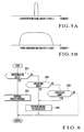
- Figs. 5A and 5B show comparison between spectra when communication schemes are switched in accordance with the communication amount in the prior for the sake of comparison with this embodiment.
- Fig. 5A shows a case wherein the communication amount is relatively small.
- Fig. 5B shows a case wherein the communication amount is relatively large.
- the general communication scheme is used even when the communication amount is relatively small, the occupied bandwidth is small in accordance with the data amount.
- the QPSK scheme is a modulation scheme of making the bit information (00, 01, 10, 11) of a baseband correspond to the phase (0°, 90°, 180°, 270°) of a carrier wave.
- Fig. 5A shows this.
- the transmission power required to maintain transmission quality i.e., the transmission power required to obtain Eb/No (the power density to noise power density ratio per bit in a digital modulated signal) required on the receiving side, is reduced to 1/128, as compared with the conventional case wherein 2,048 kbps information is transmitted at the same rate with an error correction rate of 1/2 by QPSK, because energy is spread. This corresponds to a power difference of about 21 dB.
- the transmission symbol rate is set to be the same as the rate of the chip clock 129. This is because when the communication amount is relatively large, the frequency of the read clock 133 for reading out the communication data 137 from the transmission buffer 123 shown in Fig. 2 is inevitably high.
- the center frequency of a carrier wave is set be the same as that obtained by performing spread spectrum as shown in Fig. 4B. That is, when the communication amount is relatively small, the information rate is 16 kbps, whereas the information rate is increased to 2,048 kbps to cope with a case wherein the communication amount is relatively large.
- Fig. 5B shows a case wherein the communication amount is relatively large in the prior art on the assumption that communication is performed by the same communication scheme as that used when the communication amount is relatively large in this embodiment.
- the communication interruption time required for the demodulator to perform resynchronization for a changed transmission rate at the time of switching transmission rates can be eliminated.
- This can eliminate the necessity of a buffer area for temporarily storing data associated with transmission/reception which is required to cope with a communication interruption. In this embodiment, therefore, only a minimum buffer memory for the discrimination of a communication amount is required, allowing a great reduction in buffer capacity. This makes it possible to simplify the device and reduce the cost of the device.
- the communication amount monitoring circuit 124 connected to the transmission buffer 123 determines that the communication amount is relatively large, and general PSK modulation is performed. Otherwise, when the communication amount monitoring circuit 124 determines that the communication amount is relatively small, communication is performed by the spread spectrum technique. Assume that the communication amount monitoring circuit 124 discriminates, on the basis of the same threshold, whether or not the communication amount is large. In this case, if the communication amount is an almost intermediate value of these values, information rates may be frequently switched.
- a predetermined difference may be set between a threshold by which the information rate is switched from the high rate to the low rate and a threshold by which the information rate is switched from the low rate to the high rate. More specifically, the threshold by which the information rate is switched from the high rate to the low rate is set to be smaller than the threshold by which the information rate is switched from the low rate to the high rate.
- Fig. 6 shows an example of switching control, as the third embodiment, which is performed when communication methods are switched in a cell phone in accordance with the amount of communication data.
- a CPU Central Processing Unit
- the CPU determines whether or not the general voice communication mode is set (step S201). If the general voice communication mode is set (Y), since the amount of communication data is smaller than that in another mode (to be described next), transmission is performed by using the spread spectrum technique (step S202).
- step S203 if the videophone mode is set (step S203: Y), or the Web access mode of, for example, downloading contents upon connection to the Internet (step S204: Y), the CPU determines that the amount of communication data is relatively large, and performs transmission by general PSK modulation (step S205).
- the transmission symbol rate in spread spectrum in step S202 is equal to that in PSK modulation in step S205.
- This can therefore eliminate the communication interruption time required for the demodulator to perform resynchronization for a changed transmission rate at the time of switching information rates.
- the capacity of the buffer can be further reduced.
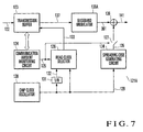
- Fig. 7 shows the arrangement of the transmission unit of a first communication device in the fourth embodiment of the present invention, and , corresponds to Fig. 2 in the first embodiment.
- the same reference numerals as in Fig. 2 denote the same parts in Fig. 7, and a description thereof will be omitted as needed.
- a transmission unit 121A of the first communication device In a transmission unit 121A of the first communication device according to the fourth embodiment, communication data 137 output from a transmission buffer 123 is directly input to a baseband modulator 139A, which in turn performs baseband modulation. Communication data 301 after modulation is input to one input terminal of an exclusive adder 136.
- the exclusive adder 136 calculates the exclusive-OR (EOR) of a spreading code 135 input to the other input terminal and the communication data 301, and inputs the addition output as a modulated output 141 to the radio communication channel 105 shown in Fig. 1.
- EOR exclusive-OR
- the transmitting side selects one of the two types of signal forms in accordance with the amount of information and transmits the information, the receiving side need not perform resynchronization of the demodulator when the signal forms are switched, because the transmission rate is not changed. This prevents any communication interruption and eliminates the necessity of a buffer area for handling such a problem.
- this eliminates the necessity of other circuits to cope with a communication interruption, and hence can achieve simplification of the circuit of the transmission/reception device and a reduction in cost. Furthermore, when the amount of information to be transmitted per unit time is relatively small, since the bandwidth is increased as compared with the prior art, stable communication can be maintained.
- the information amount magnitude discrimination means uses two different thresholds, even if the information amount takes an intermediate value, stable circuit operation can be ensured.
- the magnitude of the information amount may be discriminated in accordance with the path through which information to be transmitted is acquired or the mode used by the device instead of making the information amount magnitude discrimination means discriminate the magnitude of the information amount from the amount of information actually processed. For example, when a homepage is browsed, relatively large volume data is downloaded. When such a path is selected, therefore, communication processing is performed upon determination that the information amount is relatively large. When the device shifts to the videophone mode of performing videophone operation, relatively large volume image data is communicated. When, therefore, such a path is selected, communication processing is performed upon determination that the information amount is relatively large. This allows the execution of standardized processing, and hence saves the circuit the burden of determination. In addition, a reduction in the capacity of the buffer memory can be achieved.
Landscapes
- Engineering & Computer Science (AREA)
- Signal Processing (AREA)
- Computer Networks & Wireless Communication (AREA)
- Power Engineering (AREA)
- Communication Control (AREA)
- Digital Transmission Methods That Use Modulated Carrier Waves (AREA)
Abstract
A communication amount monitoring circuit
(124) monitors a transmission buffer (123) to which
communication data (122) is input, and discriminates the
magnitude of the amount of communication data. If the
amount of information per unit time is relatively large,
information is read out from the transmission buffer in
accordance with a chip clock. This information is
modulated as communication data (137) by a modulator
(139) and transmitted. If the amount of information is
relatively small, information is read out from the
transmission buffer (123) in accordance with a clock
obtained by frequency-dividing the chip clock. This
information is exclusive-ORed with a spreading code
generated by using the chip clock and is then modulated
by a modulator (139). The resultant data is transmitted
as communication data (137). Since there is no change
in the frequency of the communication data (137), there
is no need to provide any resynchronization on the
reception device side at the time of switching between
the large and small amounts of information. There is
therefore no need to provide any buffer area for
resynchronization.
Description
The present invention relates to a digital
communication system and, more particularly, to a
variable communication system which switches
communication schemes in accordance with the
communication amount.
In digital communication systems, there have
been various proposals to efficiently transmit data.
For example, in the digital communication system
disclosed in Japanese Patent Laid-Open No. 7-123039, the
traffic of communication is detected from an m-sequence
signal input to a rate conversion multiplexer (not
shown), and the rate conversion multiplexer multiplexes
data at a rate corresponding to the traffic. A variable
rate modulator (not shown) then modulates the
multiplexed signal and transmits it to a transmission
path at a transmission rate corresponding to the
magnitude of the traffic. That is, the modulation clock
rate is time-modulated. On the receiving side, a
variable rate demodulator (not shown) performs
demodulation, and a rate conversion demultiplexer (not
shown) demultiplexes and rate-converts the demodulated
signal to reproduce the data. Claim 2 in Japanese
Patent Laid-Open No. 2000-316035 proposes a technique of
efficiently assigning bands by dynamically changing the
transmission rate in accordance with the transmission
amount as in the above prior art.
In this manner, in the field of digital
communication systems, when the communication amount is
small, the transmission rate of information to be
transmitted is set low to set a line with a low
modulation clock rate, whereas as the communication
amount increases, a line with a high modulation clock
rate and high transmission rate is set. For example, a
router which has selected a general voice line connects
to a predetermined content server on the Internet at a
given time point to transfer large-volume data.
Likewise, when a cell phone switches to the videophone
mode during voice communication, the communication
amount increases at this time point. In a case opposite
to the above case, the communication amount decreases at
a predetermined time point.
Properly switching the transmission rates of
information in accordance with the communication amount
in this manner makes it possible to perform efficient
communication. In general, however, when the modulation
scheme to be used remains the same, if the transmission
rate is low and the modulation clock rate is low, a line
tends to relatively deteriorate because it is
susceptible to the influences of phase noise in a local
oscillator in an up converter which performs frequency
conversion to obtain carrier waves or a down converter
in a reception unit. This makes it impossible to obtain
a stable transmission path. In general, therefore, it
is preferable to use a line with a high transmission
rate and high modulation clock rate.
In contrast, it is conceivable to use a
technique of performing multilevel modulation in the
same band by different modulation schemes while the
modulation clock rate is kept constant. 16-QAM
(Quadrature Amplitude Modulation) which can obtain 16
signal states is capable of obtaining a quadruple
transmission rate at the same modulation clock rate as
compared with BPSK (Bi-Phase Shift Keying) which is a
modulation scheme of making bit information of a
baseband correspond to two phases. When, however,
multilevel modulation is to be performed, in order to
keep transmission path quality (i.e., a bit error rate)
equivalent to a modulation scheme with a low
transmission rate, it is necessary to increase the
output level by an amount equal to or more than a band
improvement in terms of transmission rate. In the above
case, although 16-QAM realizes a band improvement of 6
dB in terms of transmission rate as compared with BPSK,
the transmission carrier power must be increased by 10
dB or more to obtain the same bit error rate at 10E-6 as
that in BPSK.
In addition, when the transmission rates are
switched in accordance with the communication amount,
demodulation synchronization must be established with
respect to the transmission rate after switching at the
time of this switching operation. Demodulated data is
temporarily interrupted until demodulation
synchronization is established. Compare a case wherein
the transmission rate after switching is high with a
case wherein the transmission rare after switching is
low. In the latter case, for example, in a carrier wave
reproducing circuit, the frequency error of a reception
carrier wave with respect to the modulation clock rate
becomes relatively large. For this reason, in a PLL
circuit for carrier wave reproduction, it takes a longer
time to establish demodulation synchronization than in
the case wherein the transmission rate after switching
is high. Omission of communication data due to the
interruption of demodulated data leads to a crucial
result on the reproduction of information. In order to
prevent omission of information due to the interruption
of demodulated data, a buffer memory has been
conventionally used. There has been a communication
sequence in which when transmission or reception is to
be performed, communication data is temporarily stored
in the buffer memory, and transmission is stopped at a
predetermined timing which poses no problem in the
reproduction of information. In this sequence, when the
receiving side detects omission of communication data, a
re-transmission request is generated to read out the
corresponding portion from the buffer memory on the
transmitting side and re-transmit it.
In order to prevent omission of communication
data and guarantee the perfection of reproduction of
information by using such a technique, a considerably
large buffer memory must be prepared. If information
rates are set in two levels, i.e., a low rate and a high
rate, as in the above case, in particular, the
interruption of communication data becomes large in the
case wherein the information rate is low. In this case,
therefore, a buffer memory large enough to cover this
must be prepared.
It is an object of the present invention to
provide a variable communication system which reduces
the capacity of a buffer memory ascribed to switching of
transmission rates while switching communication schemes
in accordance with the magnitude of the communication
amount per unit time.
In order to achieve the above object,
according to the present invention, there is provided a
variable communication system characterized by
comprising (I) a transmission device including
information amount magnitude discrimination means for
discriminating whether an amount of information to be
transmitted per unit time is relatively large or small,
first communication data sending means for, when the
information amount magnitude discrimination means
discriminates that the amount of information to be
transmitted is relatively large, digitally modulating
first information as the information into information in
a signal form having a predetermined bandwidth with a
predetermined center frequency, and sending out the
information as communication data, and second
communication data sending means for, when the
information amount magnitude discrimination means
discriminates that the amount of information to be
transmitted is relatively small, digitally modulating
second information as the information upon performing
spread spectrum to obtain the same bandwidth as the
predetermined bandwidth with the center frequency, and
sending out the information as the communication data,
and (II) a reception device including demodulation means
for demodulating the communication data sent from the
transmission device, de-spreading appropriateness
discrimination means for checking whether or not a
signal after demodulation can be normally de-spread,
first information reproduction means for, when the
de-spreading appropriateness discrimination means
discriminates that de-spreading cannot be normally
performed, reproducing the first information from the
signal after demodulation by the demodulation means,
de-spreading means for, when the de-spreading
appropriateness discrimination means discriminates that
de-spreading can be normally performed, de-spreading the
signal after demodulation by the demodulation means, and
second information reproduction means for reproducing
the second information from the signal after
de-spreading by the de-spreading means.
That is, the transmission device includes the
information amount magnitude discrimination means and
discriminates whether the amount of information to be
transmitted per unit time is relatively large or small.
If it is discriminated from this discrimination result
that the information is relatively large, the first
communication data sending means digitally modulates the
first information into information in a signal form
having a predetermined bandwidth with a predetermined
center frequency, and sends out the resultant data as
communication data. In this regard, there is no
specific difference from the prior art. If the
information amount magnitude discrimination means
discriminates that the information to be transmitted is
relatively small, the second information as this
information is subjected to spread spectrum and digital
modulation to be sent out as communication data. In
this case, the necessary bandwidth is spread to the
bandwidth associated with the first signal by spread
spectrum. The center frequency of the second
information is also made equal to that of the first
information, and the second information is sent out as
communication data. This makes it unnecessary for the
demodulation means of the reception device to switch
frequencies for the first information and the second
information. The time required for this operation is
also made unnecessary. In the reception device, the
de-spreading appropriateness discrimination means checks
whether or not a signal after demodulation can be
normally de-spread. If it is determined that
de-spreading can be done, this signal is regarded as the
second information and de-spread to be reproduced. If
it is determined that de-spreading cannot be done, this
signal is regarded as the first information and
reproduced without performing any spread spectrum.
In the above variable communication system,
the transmission device may further comprise a
transmission buffer which sequentially receives
information to be transmitted and outputs the
information in synchronism with a predetermined read
clock, and the information amount magnitude
discrimination means may discriminate from an amount of
information left in the transmission buffer whether the
amount of information per unit time is relatively large
or small. In addition, the first and second
communication data sending means of the transmission
device may include chip clock generating means for
outputting a chip clock having a predetermined
frequency, transmitting-side frequency dividing means
for frequency-dividing the chip clock output from the
chip clock generating means at a predetermined frequency
division ratio, read clock selection means for, when the
information amount magnitude discrimination means
discriminates that information to be transmitted is
relatively large, setting the chip clock as the read
clock, and when the information amount magnitude
discrimination means discriminates that information to
be transmitted is relatively small, setting, as the read
clock, a clock obtained by frequency-dividing the chip
clock by the transmitting-side frequency dividing means,
spreading code generating means for receiving the chip
clock and generating a spreading code, transmitting-side
switch means which receives an output from the spreading
code generating means and is turned on only when the
information amount magnitude discrimination means
discriminates that information to be transmitted is
relatively small, transmitting-side exclusive addition
means for calculating exclusive-OR between information
output from the transmission buffer in synchronism with
the read clock and an output from the transmitting-side
switch means, and modulation means for digitally
modulating an output from the transmitting-side
exclusive addition means and transmitting the output as
the communication data. Furthermore, the de-spreading
means and the first and second information reproduction
means of the reception device may include reception
clock generating means for outputting a reception clock
identical to the chip clock, de-spreading code
generating means for generating a de-spreading code on
the basis of the reception clock output from the
reception clock generating means, receiving-side switch
means which receives an output from the de-spreading
code generating means and is turned on only when the
de-spreading appropriateness discrimination means
discriminates that de-spreading can be performed,
receiving-side exclusive addition means for calculating
exclusive-OR between an output from the receiving-side
switch means and a signal after demodulation by the
demodulation means, receiving-side frequency dividing
means for frequency-dividing the reception clock at the
predetermined frequency division ratio, write clock
selection means for, when the de-spreading
appropriateness discrimination means discriminates that
de-spreading cannot be performed, selecting the
reception clock, and when de-spreading appropriateness
discrimination means discriminates that de-spreading can
be performed, selecting and outputting a clock obtained
by frequency-dividing the reception clock by using the
receiving-side frequency dividing means, and a reception
buffer in which an output from the receiving-side
exclusive addition means is written as an input in
accordance with the write clock selected by the write
clock selection means, and data stored in the reception
buffer is set as the information to be transmitted.
That is, the transmission device includes the
transmission buffer, and the information amount
magnitude discrimination means discriminates from the
amount of information left in the transmission buffer
whether the amount of information input to the device
per unit time is relatively large or small. In
accordance with this discrimination result, the period
of a read clock for reading out data from the
transmission buffer can be changed in two levels. More
specifically, if the information amount magnitude
discrimination means discriminates that the information
to be transmitted is relatively large, a chip clock is
used as a read clock. If the information amount
magnitude discrimination means discriminates that the
amount of information is relatively small, a slow clock
is obtained by frequency-dividing this chip clock using
the transmitting-side frequency dividing means. The
data read out from the transmission buffer in this
manner becomes one input to the transmitting-side
exclusive addition means. As the other input, the
spreading code generated on the basis of the chip clock
is input through the transmitting-side switch means. In
this case, the transmitting-side switch means is a
switch which is turned on only when the information
amount magnitude discrimination means discriminates that
the information to be transmitted is relatively small.
With this arrangement, if the information amount
magnitude discrimination means determines that the
information to be transmitted is relatively large, the
modulation means outputs a signal, as communication
data, which has a bandwidth corresponding to the
information amount. If the information amount magnitude
discrimination means determines that the amount of
information is relatively small, spread spectrum is
performed to spread the bandwidth, and the resultant
data is output as communication data, which has the same
center frequency as that in the case wherein it is
determined that the amount of information is relatively
large. For this reason, the transmission rate remains
the same regardless of the form of communication data
received, the demodulation means on the reception device
side need not perform demodulation synchronization
again. If it is checked on the basis of demodulated
data after demodulation by the demodulation means
whether spread spectrum can be normally performed, and
it is determined that spread spectrum can be performed,
the sent signal is regarded as a signal sent by spread
spectrum. This signal is then de-spread and written in
the reception buffer. Otherwise, the demodulated data
after demodulation is written in this reception buffer.
In this case, the write clock selection means selects a
write clock in accordance with the rate read out from
the transmission buffer on the transmission device side.
In this manner, the information after demodulation which
is to be transmitted is obtained from the reception
buffer.
Note that the first and second communication
data sending means of the transmission device may
include chip clock generating means for outputting a
chip clock having a predetermined frequency,
transmitting-side frequency dividing means for
frequency-dividing the chip clock output from the chip
clock generating means at a predetermined frequency
division ratio, read clock selection means for, when the
information amount magnitude discrimination means
discriminates that information to be transmitted is
relatively large, setting the chip clock as the read
clock, and when the information amount magnitude
discrimination means discriminates that information to
be transmitted is relatively small, setting, as the read
clock, a clock obtained by frequency-dividing the chip
clock by the transmitting-side frequency dividing means,
modulation means for digitally modulating information
output from the transmission buffer in synchronism with
a read clock, spreading code generating means for
receiving the chip clock and generating a spreading
code, transmitting-side switch means which receives an
output from the spreading code generating means and is
turned on only when the information amount magnitude
discrimination means discriminates that information to
be transmitted is relatively small, transmitting-side
exclusive addition means for calculating exclusive-OR
between an output from the modulation means and an
output from the transmitting-side switch means and
transmitting the data as the communication data.
In addition, the reception clock generating
means of the reception device may comprise reception
clock reproduction means for reproducing a reception
clock from communication data input to the demodulation
means.
Furthermore, the information amount magnitude
discrimination means of the transmission device may set
a predetermined difference between a threshold by which
it is discriminated that an information amount is
relatively large and a threshold by which it is
discriminated that an information amount is relatively
small. More specifically, the information amount
magnitude discrimination means may set a threshold by
which it is discriminated that an information amount is
relatively large to a value larger than a threshold by
which it is discriminated that an information amount is
relatively small.
In addition, the information amount magnitude
discrimination means of the transmission device may
discriminate, depending on whether or not a path through
which information to be transmitted is acquired is a
pre-specified path, whether the amount of information to
be transmitted per unit time is relatively large or
small. Alternatively, the information amount magnitude
discrimination means may discriminate, depending on
whether or not a device which processes information to
be transmitted is set in a pre-specified mode, whether
the amount of information to be transmitted per unit
time is relatively large or small.
Furthermore, the transmission device and the
reception device may comprise a radio device.
Moreover, the transmission device may output
transmission power in proportion to a transmission rate.
When the transmission rate is low, since the
transmission power is decreased, the transmission power
density decreases by an amount corresponding to an
increase in occupied bandwidth due to spread spectrum.
The embodiments of the present invention will
be described in detail below with reference to the
accompanying drawings.
Fig. 1 shows the overall arrangement of a
variable communication system according to the first
embodiment of the present invention. This variable
communication system is formed as a communication system
in which two LANs (Local Area Networks) including a
first LAN 101 and a second LAN 102 are connected to each
other. A host computer (HOST) 103 and first router
(Router) 104 are connected to the first LAN 101. A
first communication device 106 for performing
communication with a radio communication channel 105 is
connected to the first router 104. A terminal 107
controlled by a host computer (not shown) and a second
router 108 are connected to the second LAN 102. A
second communication device 109 for performing
communication with the radio communication channel 105
is connected to the second router 108.
In this variable communication system, the
first and second communication devices 106 and 109 are
designed to monitor communication amounts when they
perform communication using the radio communication
channel 105. Each communication device performs
communication upon switching information rates depending
on whether the communication amount is relatively large
or small. Note, however, that the transfer rate of
communication data communicated through the radio
communication channel 105 is always kept constant, and
when the communication amount is relatively large, a
general PSK (Phase Shift Keying) modulation scheme is
used to transmit information. When the communication
amount is relatively small, spread-spectrum
communication is performed. Since the transfer rate of
communication data remains unchanged, even if the
communication amount varies, transmission rate
resynchronization is not required at the time of
switching transmission rates. This eliminates any
communication interruption time.
Fig. 2 shows the arrangement of the
transmission unit of the first communication device
according to this embodiment. The transmission unit of
the second communication device 109 shown in Fig. 1
basically has the same arrangement as that of the
transmission unit of the first communication device 106.
Therefore, a description of the transmission unit of the
second communication device 109 will be omitted.
A transmission unit 121 of the first
communication device includes a transmission buffer 123
which receives communication data 122 sent from the
first router 104 shown in Fig. 1. The transmission
buffer 123 is a memory with a relatively small capacity.
A communication amount monitoring circuit 124 monitors
the communication amount by checking a change in the
consumption of the buffer. The communication amount
monitoring circuit 124 then outputs a communication
amount magnitude discrimination signal 125 indicating
whether the amount of communication data 122 sent from
the first router 104 is relatively large or small. The
communication amount magnitude discrimination signal 125
is input to a read clock selector 126 and the control
terminal of a spreading code selection switch 127.
In this case, the read clock selector 126
selects either a chip clock 129 having a predetermined
frequency output from a chip clock oscillator 128 or a
frequency division output 132 from a 1/N frequency
divider 131 which frequency-divides the chip clock 129
to 1/N, and supplies it as a read clock 133 to the
transmission buffer 123. In this case, the numerical
value N is an integer equal to or more than two. The
spreading code selection switch 127 is a switch for
turning on/off the supply of a spreading code 135 output
from the spreading code generating circuit 134 to one
input terminal of an exclusive adder 136. When the
contact of the spreading code selection switch 127 is
open, a fixed value of signal "0" or signal "1" is
supplied to this input terminal of the exclusive adder
136.
The chip clock 129 is supplied to the
spreading code generating circuit 134. Communication
data 137 read out from the transmission buffer 123 in
accordance with the read clock 133 is input to the other
input terminal of the exclusive adder 136. The
exclusive adder 136 calculates the exclusive-OR (EOR) of
the input spreading code 135 and the communication data
137, and inputs an addition output 138 to a modulator
139. The modulator 139 modulates this and sends out a
modulated output 141 to the radio communication channel
105 shown in Fig. 1. In this case, the modulator 139
performs spread-spectrum modulation when the
communication amount is relatively small, and performs
general PSK modulation when the communication amount is
relatively large.
Fig. 3 shows the arrangement of the reception
unit of the second communication device according to
this embodiment. The reception unit of the first
communication device 106 shown in Fig. 1 basically has
the same arrangement as that of the reception unit of
the second communication device 109. Therefore, a
description of the reception unit of the first
communication device 106 will be omitted.
A reception unit 151 of the second
communication device includes a demodulator 153 which
receives a reception signal 152 received from the radio
communication channel 105 shown in Fig. 1 and
demodulates the signal. The demodulator 153 outputs
demodulated data 154. The demodulated data 154 becomes
one input to an exclusive adder 155 and also becomes an
input to a de-spreading synchronization circuit 156.
The demodulated data 154 is also input to a reception
clock reproducing circuit 158 to reproduce a reception
clock 159. Note that the reception clock reproducing
circuit 158 may generate a reception clock 159 having a
uniquely determined frequency without receiving the
demodulated data 154. The reception clock 159 is input
to a de-spreading code generating circuit 161, one input
terminal of a write clock selector 162, and a 1/N
frequency divider 164 which inputs a frequency division
output 163 to the other input terminal of the write
clock selector 162. The de-spreading code generating
circuit 161 generates a de-spreading code 165 on the
basis of the reception clock 159, and supplies it to a
de-spreading code selection switch 166.
The de-spreading synchronization circuit 156
checks whether or not de-spreading operation can be
normally performed on the basis of the demodulated data
154. If de-spreading operation can be normally
performed, it is discriminated that the demodulated data
154 is based on spread-spectrum communication, i.e.,
communication in a case wherein the communication amount
is relatively small. Otherwise, it is discriminated
that the demodulated data is based on communication
using the general PSK modulation scheme, i.e.,
communication in a case wherein the communication amount
is relatively large. The discrimination result is then
output as a communication amount magnitude
discrimination signal 167. The communication amount
magnitude discrimination signal 167 is supplied to the
write clock selector 162 and de-spreading code selection
switch 166. If de-spreading operation can be normally
done, the de-spreading synchronization circuit 156
outputs a synchronization timing signal 168 and supplies
it to the 1/N frequency divider 164.
When, therefore, the communication amount is
relatively small and spread spectrum is to be performed,
the contact of the de-spreading code selection switch
166 is closed by the communication amount magnitude
discrimination signal 167, and the de-spreading code 165
is input to the exclusive adder 155. The exclusive
adder 155 de-spreads the demodulated data 154 by using
the de-spreading code 165, and supplies communication
data 169 to a reception buffer 171. In this case
wherein spread spectrum is performed, the
synchronization timing signal 168 is supplied to the 1/N
frequency divider 164, and the frequency division output
163 obtained by frequency-dividing the reception clock
159 to 1/N is supplied to the write clock selector 162,
together with the reception clock 159. The write clock
selector 162 has received the communication amount
magnitude discrimination signal 167 indicating that the
communication amount is relatively small. The write
clock selector 162 therefore selects the frequency
division output 163 obtained by frequency-dividing the
reception clock 159 to 1/N and supplies it as a write
clock 172 to the reception buffer 171. When the
communication amount is relatively small and spread
spectrum is performed, therefore, the communication data
169 is sampled by the frequency division output 163
obtained by frequency-dividing the reception clock 159
to 1/N and written in the reception buffer 171.
In contrast to this, when the communication
amount is relatively large and communication is to be
performed by the general PSK modulation scheme, the
contact of the de-spreading code selection switch 166 is
opened by the communication amount magnitude
discrimination signal 167. The demodulated data 154
output from the demodulator 153 therefore passes through
the exclusive adder 155 and is supplied to the reception
buffer 171. At this time, the write clock selector 162
selects the reception clock 159 and supplies it as the
write clock 172 to the reception buffer 171. When the
communication amount is large, the communication data
169 is sampled by the write clock 172 with a high
frequency and written in the reception buffer 171. The
communication data 169 stored in the reception buffer
171 is sequentially read out as communication data 173.
Figs. 4A and 4B show comparison between
spectra when communication schemes are switched in
accordance with the communication amount in this
embodiment. Fig. 4A shows a case wherein the
communication amount is relatively small. Fig. 4B shows
a case wherein the communication amount is relatively
large. In this embodiment, when the communication
amount is relatively small, the spreading code 135
output from the spreading code generating circuit 134
shown in Fig. 2 is exclusively added to the
communication data 137 to perform spread spectrum. The
chip clock 129 at this time is N times the communication
data 137 read out from the transmission buffer 123 in
accordance with the read clock 133. Therefore, the data
to be transmitted is spread to increase the occupied
bandwidth, and is then transmitted.
Figs. 5A and 5B show comparison between
spectra when communication schemes are switched in
accordance with the communication amount in the prior
for the sake of comparison with this embodiment.
Fig. 5A shows a case wherein the communication amount is
relatively small. Fig. 5B shows a case wherein the
communication amount is relatively large. In the prior
art, since the general communication scheme is used even
when the communication amount is relatively small, the
occupied bandwidth is small in accordance with the data
amount.
Assume a case wherein 16 kbps (Kbits per
second) information exists as a case wherein the
communication amount is relatively small. When this
information is modulated by the QPSK (Quadrature Phase
Shift Keying, Quadri-Phase Shift keying) scheme and
transmitted, the transmission symbol rate becomes 16
kHz. In this case, the QPSK scheme is a modulation
scheme of making the bit information (00, 01, 10, 11) of
a baseband correspond to the phase (0°, 90°, 180°, 270°)
of a carrier wave. Fig. 5A shows this.
Assume that spread spectrum is performed as in
this embodiment. When the spreading ratio is "128", the
product of this ratio and the transmission symbol rate
becomes the frequency of the chip clock 129, which is
2,048 kHz. In the case of spread spectrum, as shown in
Fig. 4A corresponding to Fig. 5A, the necessary
bandwidth increases by 128 times. However, the
transmission power required to maintain transmission
quality, i.e., the transmission power required to obtain
Eb/No (the power density to noise power density ratio
per bit in a digital modulated signal) required on the
receiving side, is reduced to 1/128, as compared with
the conventional case wherein 2,048 kbps information is
transmitted at the same rate with an error correction
rate of 1/2 by QPSK, because energy is spread. This
corresponds to a power difference of about 21 dB.
A case wherein the communication amount is
relatively large will be described next. In this case,
according to this embodiment, general PSK modulation is
performed instead of the spread spectrum technique. The
transmission symbol rate is set to be the same as the
rate of the chip clock 129. This is because when the
communication amount is relatively large, the frequency
of the read clock 133 for reading out the communication
data 137 from the transmission buffer 123 shown in
Fig. 2 is inevitably high. In addition, in this
embodiment, the center frequency of a carrier wave is
set be the same as that obtained by performing spread
spectrum as shown in Fig. 4B. That is, when the
communication amount is relatively small, the
information rate is 16 kbps, whereas the information
rate is increased to 2,048 kbps to cope with a case
wherein the communication amount is relatively large.
In this case, assuming that the same transmission
quality as that in the case of 16 kbps is to be
maintained, the transmission output power must be
increased by 21 dB. Note that Fig. 5B shows a case
wherein the communication amount is relatively large in
the prior art on the assumption that communication is
performed by the same communication scheme as that used
when the communication amount is relatively large in
this embodiment.
As described above, in this embodiment, when
the magnitude of the transmission rate is changed in
accordance with the communication amount, i.e., the
magnitude of the traffic, since the transmission symbol
rate itself remains unchanged, the communication
interruption time required for the demodulator to
perform resynchronization for a changed transmission
rate at the time of switching transmission rates can be
eliminated. This can eliminate the necessity of a
buffer area for temporarily storing data associated with
transmission/reception which is required to cope with a
communication interruption. In this embodiment,
therefore, only a minimum buffer memory for the
discrimination of a communication amount is required,
allowing a great reduction in buffer capacity. This
makes it possible to simplify the device and reduce the
cost of the device.
In the first embodiment described above, when
the amount of communication data stored in the
transmission buffer 123, which temporarily stores the
communication data 122, becomes large, the communication
amount monitoring circuit 124 connected to the
transmission buffer 123 determines that the
communication amount is relatively large, and general
PSK modulation is performed. Otherwise, when the
communication amount monitoring circuit 124 determines
that the communication amount is relatively small,
communication is performed by the spread spectrum
technique. Assume that the communication amount
monitoring circuit 124 discriminates, on the basis of
the same threshold, whether or not the communication
amount is large. In this case, if the communication
amount is an almost intermediate value of these values,
information rates may be frequently switched. In order
to prevent such frequency switching, a predetermined
difference may be set between a threshold by which the
information rate is switched from the high rate to the
low rate and a threshold by which the information rate
is switched from the low rate to the high rate. More
specifically, the threshold by which the information
rate is switched from the high rate to the low rate is
set to be smaller than the threshold by which the
information rate is switched from the low rate to the
high rate.
Fig. 6 shows an example of switching control,
as the third embodiment, which is performed when
communication methods are switched in a cell phone in
accordance with the amount of communication data. In
this embodiment, a CPU (Central Processing Unit) (not
shown) is incorporated in the cell phone (not shown),
and the CPU executes a predetermined control program to
switch the communication methods. The CPU determines
whether or not the general voice communication mode is
set (step S201). If the general voice communication
mode is set (Y), since the amount of communication data
is smaller than that in another mode (to be described
next), transmission is performed by using the spread
spectrum technique (step S202).
In contrast to this, if the videophone mode is
set (step S203: Y), or the Web access mode of, for
example, downloading contents upon connection to the
Internet (step S204: Y), the CPU determines that the
amount of communication data is relatively large, and
performs transmission by general PSK modulation (step
S205). As in the first embodiment, the transmission
symbol rate in spread spectrum in step S202 is equal to
that in PSK modulation in step S205. This can therefore
eliminate the communication interruption time required
for the demodulator to perform resynchronization for a
changed transmission rate at the time of switching
information rates. In addition, in the third
embodiment, since whether the communication amount is
large or small is determined without using the
transmission buffer 123, unlike the first embodiment,
the capacity of the buffer can be further reduced.
Fig. 7 shows the arrangement of the
transmission unit of a first communication device in the
fourth embodiment of the present invention, and ,
corresponds to Fig. 2 in the first embodiment. The same
reference numerals as in Fig. 2 denote the same parts in
Fig. 7, and a description thereof will be omitted as
needed.
In a transmission unit 121A of the first
communication device according to the fourth embodiment,
communication data 137 output from a transmission buffer
123 is directly input to a baseband modulator 139A,
which in turn performs baseband modulation.
Communication data 301 after modulation is input to one
input terminal of an exclusive adder 136. The exclusive
adder 136 calculates the exclusive-OR (EOR) of a
spreading code 135 input to the other input terminal and
the communication data 301, and inputs the addition
output as a modulated output 141 to the radio
communication channel 105 shown in Fig. 1. Other points
are the same as those in the first embodiment.
In the above embodiment, when the amount of
communication data is relatively large, general PSK
modulation is performed. Obviously, however, if the
clock frequency is the same as the frequency of a chip
clock used for spread spectrum, information may be
modulated by another modulation scheme.
As has been described above, according to the
above embodiment, when it is discriminated that the
amount of information to be transmitted per unit time is
relatively small, spread spectrum is performed to
increase the bandwidth to allow transmission with the
same bandwidth and the same center frequency as in the
case wherein the amount of information to be transmitted
is large. For this reason, in spite of the fact that
the transmitting side selects one of the two types of
signal forms in accordance with the amount of
information and transmits the information, the receiving
side need not perform resynchronization of the
demodulator when the signal forms are switched, because
the transmission rate is not changed. This prevents any
communication interruption and eliminates the necessity
of a buffer area for handling such a problem. In
addition, this eliminates the necessity of other
circuits to cope with a communication interruption, and
hence can achieve simplification of the circuit of the
transmission/reception device and a reduction in cost.
Furthermore, when the amount of information to be
transmitted per unit time is relatively small, since the
bandwidth is increased as compared with the prior art,
stable communication can be maintained.
In addition, since the information amount
magnitude discrimination means uses two different
thresholds, even if the information amount takes an
intermediate value, stable circuit operation can be
ensured.
Furthermore, the magnitude of the information
amount may be discriminated in accordance with the path
through which information to be transmitted is acquired
or the mode used by the device instead of making the
information amount magnitude discrimination means
discriminate the magnitude of the information amount
from the amount of information actually processed. For
example, when a homepage is browsed, relatively large
volume data is downloaded. When such a path is
selected, therefore, communication processing is
performed upon determination that the information amount
is relatively large. When the device shifts to the
videophone mode of performing videophone operation,
relatively large volume image data is communicated.
When, therefore, such a path is selected, communication
processing is performed upon determination that the
information amount is relatively large. This allows the
execution of standardized processing, and hence saves
the circuit the burden of determination. In addition, a
reduction in the capacity of the buffer memory can be
achieved.
Claims (12)
- A variable communication system characterized by comprising:a transmission device including information amount magnitude discrimination means for discriminating whether an amount of information to be transmitted per unit time is relatively large or small, first communication data sending means for, when said information amount magnitude discrimination means discriminates that the amount of information to be transmitted is relatively large, digitally modulating first information as the information into information in a signal form having a predetermined bandwidth with a predetermined center frequency, and sending out the information as communication data, and second communication data sending means for, when said information amount magnitude discrimination means discriminates that the amount of information to be transmitted is relatively small, digitally modulating second information as the information upon performing spread spectrum to obtain the same bandwidth as the predetermined bandwidth with the center frequency, and sending out the information as the communication data, anda reception device including demodulation means for demodulating the communication data sent from said transmission device, de-spreading appropriateness discrimination means for checking whether or not a signal after demodulation can be normally de-spread, first information reproduction means for, when said de-spreading appropriateness discrimination means discriminates that de-spreading cannot be normally performed, reproducing the first information from the signal after demodulation by said demodulation means, de-spreading means for, when said de-spreading appropriateness discrimination means discriminates that de-spreading can be normally performed, de-spreading the signal after demodulation by said demodulation means, and second information reproduction means for reproducing the second information from the signal after de-spreading by said de-spreading means.
- A variable communication system according to claim 1, characterized in that
said transmission device further comprises a transmission buffer which sequentially receives information to be transmitted and outputs the information in synchronism with a predetermined read clock, and
said information amount magnitude discrimination means discriminates from an amount of information left in said transmission buffer whether the amount of information per unit time is relatively large or small. - A variable communication system according to claim 2, characterized in that said first and second communication data sending means include chip clock generating means for outputting a chip clock having a predetermined frequency, transmitting-side frequency dividing means for frequency-dividing the chip clock output from said chip clock generating means at a predetermined frequency division ratio, read clock selection means for, when said information amount magnitude discrimination means discriminates that information to be transmitted is relatively large, setting the chip clock as the read clock, and when said information amount magnitude discrimination means discriminates that information to be transmitted is relatively small, setting, as the read clock, a clock obtained by frequency-dividing the chip clock by said transmitting-side frequency dividing means, spreading code generating means for receiving the chip clock and generating a spreading code, transmitting-side switch means which receives an output from said spreading code generating means and is turned on only when said information amount magnitude discrimination means discriminates that information to be transmitted is relatively small, transmitting-side exclusive addition means for calculating exclusive-OR between information output from said transmission buffer in synchronism with the read clock and an output from said transmitting-side switch means, and modulation means for digitally modulating an output from said transmitting-side exclusive addition means and transmitting the output as the communication data.
- A variable communication system according to claim 2, characterized in that said first and second communication data sending means include chip clock generating means for outputting a chip clock having a predetermined frequency, transmitting-side frequency dividing means for frequency-dividing the chip clock output from said chip clock generating means at a predetermined frequency division ratio, read clock selection means for, when said information amount magnitude discrimination means discriminates that information to be transmitted is relatively large, setting the chip clock as the read clock, and when said information amount magnitude discrimination means discriminates that information to be transmitted is relatively small, setting, as the read clock, a clock obtained by frequency-dividing the chip clock by said transmitting-side frequency dividing means, modulation means for digitally modulating information output from said transmission buffer in synchronism with a read clock, spreading code generating means for receiving the chip clock and generating a spreading code, transmitting-side switch means which receives an output from said spreading code generating means and is turned on only when said information amount magnitude discrimination means discriminates that information to be transmitted is relatively small, transmitting-side exclusive addition means for calculating exclusive-OR between an output from said modulation means and an output from said transmitting-side switch means and transmitting the data as the communication data.
- A variable communication system according to claim 3, characterized in that said de-spreading means and said first and second information reproduction means include reception clock generating means for outputting a reception clock identical to the chip clock, de-spreading code generating means for generating a de-spreading code on the basis of the reception clock output from said reception clock generating means, receiving-side switch means which receives an output from said de-spreading code generating means and is turned on only when said de-spreading appropriateness discrimination means discriminates that de-spreading can be performed, receiving-side exclusive addition means for calculating exclusive-OR between an output from said receiving-side switch means and a signal after demodulation by said demodulation means, receiving-side frequency dividing means for frequency-dividing the reception clock at the predetermined frequency division ratio, write clock selection means for, when said de-spreading appropriateness discrimination means discriminates that de-spreading cannot be performed, selecting the reception clock, and when de-spreading appropriateness discrimination means discriminates that de-spreading can be performed, selecting and outputting a clock obtained by frequency-dividing the reception clock by using said receiving-side frequency dividing means, and a reception buffer in which an output from said receiving-side exclusive addition means is written as an input in accordance with the write clock selected by said write clock selection means, and data stored in said reception buffer is set as the information to be transmitted.
- A variable communication system according to claim 5, characterized in that said reception clock generating means comprises reception clock reproduction means for reproducing a reception clock from communication data input to said demodulation means.
- A variable communication system according to claim 2, characterized in that said information amount magnitude discrimination means sets a predetermined difference between a threshold by which it is discriminated that an information amount is relatively large and a threshold by which it is discriminated that an information amount is relatively small.
- A variable communication system according to claim 7, characterized in that said information amount magnitude discrimination means sets a threshold by which it is discriminated that an information amount is relatively large to a value larger than a threshold by which it is discriminated that an information amount is relatively small.
- A variable communication system according to claim 1, characterized in that said information amount magnitude discrimination means discriminates, depending on whether or not a path through which information to be transmitted is acquired is a pre-specified path, whether the amount of information to be transmitted per unit time is relatively large or small.
- A variable communication system according to claim 1, characterized in that said information amount magnitude discrimination means discriminates, depending on whether or not a device which processes information to be transmitted is set in a pre-specified mode, whether the amount of information to be transmitted per unit time is relatively large or small.
- A variable communication system according to claim 1, characterized in that said transmission device and said reception device comprise a radio device.
- A variable communication system according to claim 1, characterized in that said transmission device outputs transmission power in proportion to a transmission rate.
Applications Claiming Priority (3)
| Application Number | Priority Date | Filing Date | Title |
|---|---|---|---|
| JP2002062039A JP3896873B2 (en) | 2002-03-07 | 2002-03-07 | Variable communication system |
| JP2002062039 | 2002-03-07 | ||
| PCT/JP2003/002739 WO2003081799A1 (en) | 2002-03-07 | 2003-03-07 | Variable communication system |
Publications (2)
| Publication Number | Publication Date |
|---|---|
| EP1482653A1 true EP1482653A1 (en) | 2004-12-01 |
| EP1482653A4 EP1482653A4 (en) | 2008-04-23 |
Family
ID=28449049
Family Applications (1)
| Application Number | Title | Priority Date | Filing Date |
|---|---|---|---|
| EP03744722A Withdrawn EP1482653A4 (en) | 2002-03-07 | 2003-03-07 | Variable communication system |
Country Status (5)
| Country | Link |
|---|---|
| US (1) | US7123888B2 (en) |
| EP (1) | EP1482653A4 (en) |
| JP (1) | JP3896873B2 (en) |
| AU (1) | AU2003211842A1 (en) |
| WO (1) | WO2003081799A1 (en) |
Families Citing this family (6)
| Publication number | Priority date | Publication date | Assignee | Title |
|---|---|---|---|---|
| EP1521412B1 (en) | 2003-09-30 | 2007-03-07 | Siemens Aktiengesellschaft | Switching between communication systems with circuit and packet switching |
| JP4641714B2 (en) * | 2003-11-12 | 2011-03-02 | ソニー株式会社 | Remote monitoring system |
| US7472306B2 (en) * | 2004-05-18 | 2008-12-30 | Intel Corporation | Processor timing apparatus, systems, and methods |
| US8312267B2 (en) | 2004-07-20 | 2012-11-13 | Time Warner Cable Inc. | Technique for securely communicating programming content |
| JP2007281549A (en) * | 2006-04-03 | 2007-10-25 | Sumitomo Electric Ind Ltd | Management device, management method, and local area network |
| KR101564913B1 (en) * | 2008-09-17 | 2015-11-03 | 삼성전자 주식회사 | Communication method for air conditioner |
Family Cites Families (11)
| Publication number | Priority date | Publication date | Assignee | Title |
|---|---|---|---|---|
| JPH0786981A (en) * | 1993-09-10 | 1995-03-31 | Nippon Hoso Kyokai <Nhk> | Digital signal transmission method |
| JP2626509B2 (en) | 1993-10-25 | 1997-07-02 | 日本電気株式会社 | Digital satellite communication system |
| JPH07245574A (en) | 1994-03-07 | 1995-09-19 | Nippon Hoso Kyokai <Nhk> | Digital signal transmission method |
| US6496543B1 (en) * | 1996-10-29 | 2002-12-17 | Qualcomm Incorporated | Method and apparatus for providing high speed data communications in a cellular environment |
| JPH11215175A (en) * | 1998-01-22 | 1999-08-06 | Brother Ind Ltd | Document information transmission system and document information transmission device |
| JP2000092009A (en) * | 1998-07-13 | 2000-03-31 | Sony Corp | Communication method, transmitter and receiver |
| JP3380515B2 (en) * | 1999-04-02 | 2003-02-24 | 松下電器産業株式会社 | Communication terminal device and signal determination method in communication terminal device |
| US6754189B1 (en) | 1999-04-08 | 2004-06-22 | Lucent Technologies Inc. | Method of queue length based burst management in wireless communication systems |
| KR100594042B1 (en) * | 1999-09-22 | 2006-06-28 | 삼성전자주식회사 | Apparatus and method for generating multi scrambling code in asynchronous mobile communication system |
| DE10004873A1 (en) * | 2000-02-04 | 2001-08-23 | Infineon Technologies Ag | Method and device for generating OVSF code words |
| US20030086503A1 (en) * | 2001-11-08 | 2003-05-08 | Koninklijke Philips Electronics N.V. | Apparatus and method for passing large bitwidth data over a low bitwidth datapath |
-
2002
- 2002-03-07 JP JP2002062039A patent/JP3896873B2/en not_active Expired - Fee Related
-
2003
- 2003-03-07 WO PCT/JP2003/002739 patent/WO2003081799A1/en not_active Ceased
- 2003-03-07 AU AU2003211842A patent/AU2003211842A1/en not_active Abandoned
- 2003-03-07 EP EP03744722A patent/EP1482653A4/en not_active Withdrawn
- 2003-03-07 US US10/506,623 patent/US7123888B2/en not_active Expired - Fee Related
Also Published As
| Publication number | Publication date |
|---|---|
| WO2003081799A1 (en) | 2003-10-02 |
| JP2003264479A (en) | 2003-09-19 |
| US20050107050A1 (en) | 2005-05-19 |
| AU2003211842A1 (en) | 2003-10-08 |
| EP1482653A4 (en) | 2008-04-23 |
| JP3896873B2 (en) | 2007-03-22 |
| US7123888B2 (en) | 2006-10-17 |
Similar Documents
| Publication | Publication Date | Title |
|---|---|---|
| US7486634B2 (en) | Adaptive modulation based on signal quality | |
| US10270631B2 (en) | Transmission apparatus, reception apparatus and digital radio communication method | |
| CN100490367C (en) | base station device and terminal device | |
| EP1274208A1 (en) | Communication device and transmission mode selecting method | |
| JPH11178050A (en) | Control information transmission method, transmission device, and transmission / reception device | |
| US7366543B2 (en) | Method for allocating channels, and base station apparatus and communication system utilizing the channel allocating method | |
| EP1480364B1 (en) | Communication device used in cdma | |
| US8255558B2 (en) | Method and system for distributed infrastructure for streaming data via multiple access points | |
| US7123888B2 (en) | Variable communication system | |
| US7180962B2 (en) | Apparatus and method for demodulation using detection of channel adaptive modulation scheme | |
| JP5532055B2 (en) | Wireless communication apparatus, wireless communication system, and wireless communication method | |
| US7333550B2 (en) | Bit processing method for adaptive multirate modulation | |
| JPH09172391A (en) | Spread spectrum communication system | |
| JP2005130296A (en) | Receiving device and call signal receiving method | |
| JPH11177641A (en) | Control information allocation method, control method, transmission method, reception method, transmission device, and reception device | |
| EP1535440A1 (en) | Embedded keying | |
| JP2793985B2 (en) | Variable-capacity spread spectrum transmitter | |
| JP2000183988A (en) | Demodulation circuit | |
| JP5200002B2 (en) | Modulation pattern compression technique for adaptive bit loading. |
Legal Events
| Date | Code | Title | Description |
|---|---|---|---|
| PUAI | Public reference made under article 153(3) epc to a published international application that has entered the european phase |
Free format text: ORIGINAL CODE: 0009012 |
|
| 17P | Request for examination filed |
Effective date: 20040902 |
|
| AK | Designated contracting states |
Kind code of ref document: A1 Designated state(s): AT BE BG CH CY CZ DE DK EE ES FI FR GB GR HU IE IT LI LU MC NL PT RO SE SI SK TR |
|
| A4 | Supplementary search report drawn up and despatched |
Effective date: 20080325 |
|
| 17Q | First examination report despatched |
Effective date: 20090420 |
|
| STAA | Information on the status of an ep patent application or granted ep patent |
Free format text: STATUS: THE APPLICATION HAS BEEN WITHDRAWN |
|
| 18W | Application withdrawn |
Effective date: 20100708 |