EP1475848A1 - Process for defining a chalcogenide material layer, in particular in a process for manufacturing phase change memory cells - Google Patents
Process for defining a chalcogenide material layer, in particular in a process for manufacturing phase change memory cells Download PDFInfo
- Publication number
- EP1475848A1 EP1475848A1 EP03425293A EP03425293A EP1475848A1 EP 1475848 A1 EP1475848 A1 EP 1475848A1 EP 03425293 A EP03425293 A EP 03425293A EP 03425293 A EP03425293 A EP 03425293A EP 1475848 A1 EP1475848 A1 EP 1475848A1
- Authority
- EP
- European Patent Office
- Prior art keywords
- layer
- process according
- etching
- chalcogenide material
- material layer
- Prior art date
- Legal status (The legal status is an assumption and is not a legal conclusion. Google has not performed a legal analysis and makes no representation as to the accuracy of the status listed.)
- Granted
Links
- 239000000463 material Substances 0.000 title claims abstract description 30
- 238000000034 method Methods 0.000 title claims abstract description 30
- 230000008569 process Effects 0.000 title claims abstract description 28
- 150000004770 chalcogenides Chemical class 0.000 title claims abstract description 19
- 238000004519 manufacturing process Methods 0.000 title claims description 4
- 230000008859 change Effects 0.000 title abstract description 10
- 229910016570 AlCu Inorganic materials 0.000 claims abstract description 23
- ZAMOUSCENKQFHK-UHFFFAOYSA-N Chlorine atom Chemical compound [Cl] ZAMOUSCENKQFHK-UHFFFAOYSA-N 0.000 claims abstract description 11
- 239000000460 chlorine Substances 0.000 claims abstract description 11
- 229910052801 chlorine Inorganic materials 0.000 claims abstract description 11
- 238000005530 etching Methods 0.000 claims description 39
- 229910052751 metal Inorganic materials 0.000 claims description 14
- 239000002184 metal Substances 0.000 claims description 14
- 238000002161 passivation Methods 0.000 claims description 12
- KZBUYRJDOAKODT-UHFFFAOYSA-N Chlorine Chemical compound ClCl KZBUYRJDOAKODT-UHFFFAOYSA-N 0.000 claims description 11
- ATJFFYVFTNAWJD-UHFFFAOYSA-N Tin Chemical compound [Sn] ATJFFYVFTNAWJD-UHFFFAOYSA-N 0.000 claims description 9
- 229910015844 BCl3 Inorganic materials 0.000 claims description 7
- FAQYAMRNWDIXMY-UHFFFAOYSA-N trichloroborane Chemical compound ClB(Cl)Cl FAQYAMRNWDIXMY-UHFFFAOYSA-N 0.000 claims description 7
- 239000004065 semiconductor Substances 0.000 claims description 3
- XLYOFNOQVPJJNP-UHFFFAOYSA-N water Chemical compound O XLYOFNOQVPJJNP-UHFFFAOYSA-N 0.000 claims description 3
- 238000001312 dry etching Methods 0.000 claims 6
- 229920002120 photoresistant polymer Polymers 0.000 claims 1
- 239000010410 layer Substances 0.000 description 66
- 239000000758 substrate Substances 0.000 description 10
- VSCWAEJMTAWNJL-UHFFFAOYSA-K aluminium trichloride Chemical compound Cl[Al](Cl)Cl VSCWAEJMTAWNJL-UHFFFAOYSA-K 0.000 description 6
- 239000007789 gas Substances 0.000 description 6
- 239000000203 mixture Substances 0.000 description 5
- 230000007797 corrosion Effects 0.000 description 4
- 238000005260 corrosion Methods 0.000 description 4
- 238000004377 microelectronic Methods 0.000 description 4
- TWNQGVIAIRXVLR-UHFFFAOYSA-N oxo(oxoalumanyloxy)alumane Chemical compound O=[Al]O[Al]=O TWNQGVIAIRXVLR-UHFFFAOYSA-N 0.000 description 4
- 239000000126 substance Substances 0.000 description 4
- 238000012360 testing method Methods 0.000 description 4
- 230000004888 barrier function Effects 0.000 description 3
- 238000001020 plasma etching Methods 0.000 description 3
- QVGXLLKOCUKJST-UHFFFAOYSA-N atomic oxygen Chemical compound [O] QVGXLLKOCUKJST-UHFFFAOYSA-N 0.000 description 2
- 238000006243 chemical reaction Methods 0.000 description 2
- 230000006378 damage Effects 0.000 description 2
- 229910052760 oxygen Inorganic materials 0.000 description 2
- 239000001301 oxygen Substances 0.000 description 2
- 239000011241 protective layer Substances 0.000 description 2
- 230000036632 reaction speed Effects 0.000 description 2
- 229910052714 tellurium Inorganic materials 0.000 description 2
- VEXZGXHMUGYJMC-UHFFFAOYSA-M Chloride anion Chemical compound [Cl-] VEXZGXHMUGYJMC-UHFFFAOYSA-M 0.000 description 1
- PXGOKWXKJXAPGV-UHFFFAOYSA-N Fluorine Chemical compound FF PXGOKWXKJXAPGV-UHFFFAOYSA-N 0.000 description 1
- XPDWGBQVDMORPB-UHFFFAOYSA-N Fluoroform Chemical compound FC(F)F XPDWGBQVDMORPB-UHFFFAOYSA-N 0.000 description 1
- 229910000927 Ge alloy Inorganic materials 0.000 description 1
- UFHFLCQGNIYNRP-UHFFFAOYSA-N Hydrogen Chemical compound [H][H] UFHFLCQGNIYNRP-UHFFFAOYSA-N 0.000 description 1
- 206010034972 Photosensitivity reaction Diseases 0.000 description 1
- 229910001245 Sb alloy Inorganic materials 0.000 description 1
- 229910001215 Te alloy Inorganic materials 0.000 description 1
- 229910045601 alloy Inorganic materials 0.000 description 1
- 239000000956 alloy Substances 0.000 description 1
- WUKWITHWXAAZEY-UHFFFAOYSA-L calcium difluoride Chemical compound [F-].[F-].[Ca+2] WUKWITHWXAAZEY-UHFFFAOYSA-L 0.000 description 1
- 239000003795 chemical substances by application Substances 0.000 description 1
- 150000001805 chlorine compounds Chemical class 0.000 description 1
- AFYPFACVUDMOHA-UHFFFAOYSA-N chlorotrifluoromethane Chemical compound FC(F)(F)Cl AFYPFACVUDMOHA-UHFFFAOYSA-N 0.000 description 1
- 239000011247 coating layer Substances 0.000 description 1
- 150000001875 compounds Chemical class 0.000 description 1
- 238000000151 deposition Methods 0.000 description 1
- 238000011161 development Methods 0.000 description 1
- 238000007865 diluting Methods 0.000 description 1
- 238000010292 electrical insulation Methods 0.000 description 1
- 229910052731 fluorine Inorganic materials 0.000 description 1
- 239000011737 fluorine Substances 0.000 description 1
- 239000010436 fluorite Substances 0.000 description 1
- 239000008246 gaseous mixture Substances 0.000 description 1
- 238000010438 heat treatment Methods 0.000 description 1
- 239000001257 hydrogen Substances 0.000 description 1
- 229910052739 hydrogen Inorganic materials 0.000 description 1
- 230000006872 improvement Effects 0.000 description 1
- 230000000873 masking effect Effects 0.000 description 1
- 239000007769 metal material Substances 0.000 description 1
- 238000012986 modification Methods 0.000 description 1
- 230000004048 modification Effects 0.000 description 1
- 229920000620 organic polymer Polymers 0.000 description 1
- 230000003647 oxidation Effects 0.000 description 1
- 238000007254 oxidation reaction Methods 0.000 description 1
- 230000001590 oxidative effect Effects 0.000 description 1
- 230000000737 periodic effect Effects 0.000 description 1
- 230000036211 photosensitivity Effects 0.000 description 1
- 230000005855 radiation Effects 0.000 description 1
- 230000009467 reduction Effects 0.000 description 1
- 229910052711 selenium Inorganic materials 0.000 description 1
- 238000000926 separation method Methods 0.000 description 1
- 238000010561 standard procedure Methods 0.000 description 1
- 239000010409 thin film Substances 0.000 description 1
- 239000003039 volatile agent Substances 0.000 description 1
- 238000001039 wet etching Methods 0.000 description 1
Images
Classifications
-
- C—CHEMISTRY; METALLURGY
- C23—COATING METALLIC MATERIAL; COATING MATERIAL WITH METALLIC MATERIAL; CHEMICAL SURFACE TREATMENT; DIFFUSION TREATMENT OF METALLIC MATERIAL; COATING BY VACUUM EVAPORATION, BY SPUTTERING, BY ION IMPLANTATION OR BY CHEMICAL VAPOUR DEPOSITION, IN GENERAL; INHIBITING CORROSION OF METALLIC MATERIAL OR INCRUSTATION IN GENERAL
- C23F—NON-MECHANICAL REMOVAL OF METALLIC MATERIAL FROM SURFACE; INHIBITING CORROSION OF METALLIC MATERIAL OR INCRUSTATION IN GENERAL; MULTI-STEP PROCESSES FOR SURFACE TREATMENT OF METALLIC MATERIAL INVOLVING AT LEAST ONE PROCESS PROVIDED FOR IN CLASS C23 AND AT LEAST ONE PROCESS COVERED BY SUBCLASS C21D OR C22F OR CLASS C25
- C23F4/00—Processes for removing metallic material from surfaces, not provided for in group C23F1/00 or C23F3/00
-
- H—ELECTRICITY
- H10—SEMICONDUCTOR DEVICES; ELECTRIC SOLID-STATE DEVICES NOT OTHERWISE PROVIDED FOR
- H10N—ELECTRIC SOLID-STATE DEVICES NOT OTHERWISE PROVIDED FOR
- H10N70/00—Solid-state devices having no potential barriers, and specially adapted for rectifying, amplifying, oscillating or switching
- H10N70/011—Manufacture or treatment of multistable switching devices
- H10N70/061—Shaping switching materials
- H10N70/063—Shaping switching materials by etching of pre-deposited switching material layers, e.g. lithography
-
- H—ELECTRICITY
- H10—SEMICONDUCTOR DEVICES; ELECTRIC SOLID-STATE DEVICES NOT OTHERWISE PROVIDED FOR
- H10N—ELECTRIC SOLID-STATE DEVICES NOT OTHERWISE PROVIDED FOR
- H10N70/00—Solid-state devices having no potential barriers, and specially adapted for rectifying, amplifying, oscillating or switching
- H10N70/20—Multistable switching devices, e.g. memristors
- H10N70/231—Multistable switching devices, e.g. memristors based on solid-state phase change, e.g. between amorphous and crystalline phases, Ovshinsky effect
-
- H—ELECTRICITY
- H10—SEMICONDUCTOR DEVICES; ELECTRIC SOLID-STATE DEVICES NOT OTHERWISE PROVIDED FOR
- H10N—ELECTRIC SOLID-STATE DEVICES NOT OTHERWISE PROVIDED FOR
- H10N70/00—Solid-state devices having no potential barriers, and specially adapted for rectifying, amplifying, oscillating or switching
- H10N70/801—Constructional details of multistable switching devices
- H10N70/821—Device geometry
- H10N70/826—Device geometry adapted for essentially vertical current flow, e.g. sandwich or pillar type devices
-
- H—ELECTRICITY
- H10—SEMICONDUCTOR DEVICES; ELECTRIC SOLID-STATE DEVICES NOT OTHERWISE PROVIDED FOR
- H10N—ELECTRIC SOLID-STATE DEVICES NOT OTHERWISE PROVIDED FOR
- H10N70/00—Solid-state devices having no potential barriers, and specially adapted for rectifying, amplifying, oscillating or switching
- H10N70/801—Constructional details of multistable switching devices
- H10N70/881—Switching materials
- H10N70/882—Compounds of sulfur, selenium or tellurium, e.g. chalcogenides
- H10N70/8828—Tellurides, e.g. GeSbTe
Definitions
- the present invention relates to a process for defining a chalcogenide material layer, in particular in a process for manufacturing phase change memory cells.
- phase change memory cells utilize a class of materials that have the unique property of being reversibly switchable from one phase to another with measurable distinct electrical properties associated with each phase. For example, these materials may change between an amorphous disordered phase and a crystalline, or polycrystalline, ordered phase.
- a material property that may change and provide a signature for each phase is the material resistivity, which is considerably different in the two states.
- a thin film of chalcogenic material may be employed as a programmable resistor, switching between a high and a low resistance condition.
- the phase of a chalcogenide material may be modified by passing electrical currents of suitable values for preset times. Furthermore, the state of the chalcogenic material may be read by applying a sufficiently small voltage (or current) so as not to cause a sensible heating and measuring the current passing through it (or voltage across it). Since the current is proportional to the conductance (or voltage is proportional to the resistance) of the chalcogenic material, it is possible to discriminate between the two phases.
- alloys of elements of group VI of the periodic table such as Te or Se, referred to as chalcogenides or chalcogenic materials, can advantageously be used in phase change memory cells.
- the currently most promising chalcogenide is formed by a Ge, Sb and Te alloy (Ge 2 Sb 2 Te 5 ), also called GST, which is currently widely used for storing information in overwritable disks.
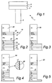
- a PCM element 1 The basic structure of a PCM element 1 is shown in Figure 1 and comprises a first electrode 2 of resistive type, forming a heater; a programmable element 3, in contact with the first electrode 2; and a second electrode 5 of a metal material, for example AlCu.
- a barrier layer 4, for example of Ti/TiN, is generally arranged between the programmable element 3 and the second electrode 5.
- barrier layer 4 and the second electrode 5 gives rise to some difficulties.
- chalcogenic materials are mainly used in microelectronic field to improve the definition of structures in the substrate.
- chalcogenide layers are used in addition to lithographic masks and act directly as masking layers since they have particular properties as regards photosensitivity and photolithographic development.
- the ability of the chalcogenic material is exploited to form compounds that are particularly reactive with the substrate to be defined, both as regards plasma etching and etching in aqueous e/o organic solution.
- the multilayer obtained by depositing the chalcogenic material on the substrate to be defined is exposed to a radiation through a standard lithographic mask, which defines only the areas where the substrate is to be exposed.
- the reaction between the remaining chalcogenic material and the substrate forms a third component that is more reactive to a wet or plasma etching.
- the chemicals used for plasma etching include fluorinated gases, such as CF 4 , CHF 3 , C 2 F 8 , CClF 3 or mixtures of O 2 , N 2 , and Ar.
- the chalcogenic layer is used to define the underlying substrate and not as the layer to be defined to form an active region.
- the used chemicals (as said, based on fluorinate gases or mixtures of O 2 , N 2 , and Ar) are not compatible with metal layers of AlCu, Ti and TiN.
- the fluorinate gases are able to etch the AlCu layer, the reaction speed is low.
- structures of AlCu exposed to a CF 4 plasma for some tens of seconds, present holes in the lower part, due to an overetching by fluorine.
- a CF 4 plasma etches heavily also TiN on the upper part of the structure.
- the object of the invention is thus to provide a process for defining GST layers.
- a process for defining a chalcogenide material layer in the manufacture of a semiconductor integrated device as defined in claim 1.
- a GST layer is dry etched using a gas mixture based on chlorine, typically a mixture of Cl 2 and BCl 3 . Etching tests made on GST layers showed very high etching speeds and very reproducible and reliable profiles.
- the same chemical mixture may be used to etch a stack including a metal layer overlying a GST layer, using an integrated etching technique and thus a same etching chamber for all the layers. Thereby, defectivity may be reduced.
- the AlCu layer is passivated before etching the underlying layers.
- the further etching of the GST layer is carried out at a lower temperature.
- a further improvement to obtain a greater control of the profile and avoid lateral overetching is obtained adding Ar, O 2 and N 2 to the etching plasma.
- Ar dilutes Cl 2 and helps in avoiding a lateral overetching of the GST layer.
- N 2 and O 2 form a protective layer of on GST lateral wall.
- a stack 10 is deposited on a substrate, according to standard techniques.
- the stack and the substrate are part of a wafer 30 ( Figure 6a).
- the stack 10 comprises, from below, an oxide layer 11, e.g. 200 nm; a first Ti layer 12, e.g. 20 nm; a GST layer 13, e.g. 60 nm; a second Ti layer 14, e.g. 5 nm; a first TiN layer 15, e.g. 20 nm; a third Ti layer 16, e.g. 10 nm; an AlCu layer 17, e.g. 220 nm; a second TiN layer 18, e.g. 15 nm; and a bottom anti-reflecting coating layer (also called BARC layer 19), e.g. 60 nm.
- BARC layer 19 bottom anti-reflecting coating layer
- the Ti layers 12, 14, 16 have the aim of improving the adhesion of the overlaying layer to the underlying layer; the first TiN layer 15 is intended to act as a barrier between AlCu layer 17 and the GST layer 13, the second TiN layer 18 has an anti-reflecting goal; the BARC layer 19 is for example an organic polymeric compound.
- a resist mask 20 is formed over the stack 10, according to the structure to be defined, in a per se known manner.
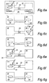
- the wafer 30 including the stack 10 is brought in an etching chamber 31 belonging to a cluster 35, as shown in Figure 6a, and a first etching step is carried out.
- the first etching uses a plasma fed by Cl 2 , BCl 3 and N 2 and is carried out at a temperature comprised between 45°C and 55°C, preferably 50°C.
- the BARC layer 19, the second TiN layer 18, the AlCu layer 17, the third Ti layer 16, the first TiN layer 15 and part of the second Ti layer 14 are selectively removed.
- the structure of Figure 3 is thus obtained.
- FIG. 6b the wafer 30 is moved in a passivation chamber 32 of the same cluster 35.
- the passivation chamber 32 is separated from etching chamber 31 but is connected thereto so as to avoid any contact with the atmosphere.
- the separation between etching chamber 31 and passivation chamber 32 is shown schematically in Figure 6a by a diaphragm 33 that is open and thus not shown in Figure 6b.
- the wafer 30 is submitted to a water vapor plasma, Figure 6c. Thereby a protective layer of aluminum oxide (Al 2 O 3 ) is formed on the lateral wall of the AlCu layer 17; furthermore, the adsorbed C1 (which reacts with hydrogen and forms HC1) and the remaining AlCl 3 are removed.
- Al 2 O 3 aluminum oxide
- a thin passivation layer 40 of aluminum oxide (Al 2 O 3 ) is formed on the lateral sides of the AlCu layer 17, as shown schematically in the enlarged detail of Figure 4.
- the wafer 30 is transferred back to the etching chamber 31, Figure 6d and subject to a second etching step, Figure 6e.
- the bottom portion of the second Ti layer 14, the GST layer 13 and an upper portion of the first Ti layer 12 are etched using a Cl 2 , BCl 3 , Ar, O 2 and N 2 plasma at a temperature comprised between 20°C and 35°C, preferably 20°C.
- the etching agents are Cl 2 , BCl 3 ; Ar, O 2 and N 2 are added to ensure the best obtainable verticality of the GST layer 13.
- Ar has the aim of diluting chlorine and avoid overetching of the GST layer 13 wall.
- Oxygen has the aim of oxidizing the exposed chalcogenic material as the etching proceeds. Oxidation of the chalcogenic material is thermodynamically favored and the reaction speed is very high.
- the oxide formed during the etching is inert to the overetching due to Cl 2 .
- stable and volatile chlorides of Ge, Sb and Te are formed; these chloride allow reaction to go on since they may easily be removed from the substrate.
- the AlCu layer 17 is protected by the thin passivation layer 40.
- the bottom portion of the first Ti layer 12 and a top portion of the oxide layer 11 are dry etched using Cl 2 , BCl 3 at a temperature comprised between 20°C and 35°C, preferably 20°C. Partial removal of the oxide layer 11 is necessary to ensure electrical insulation of the remained stack from other adjacent structures (not shown). The resulting structure is shown in Figure 5.
- the wafer 30 is transferred back to the passivation chamber 32 ( Figure 6g), where any chlorine residual that may trigger corrosion and destroy the defined structures is removed.
- the mask 20 is also removed using an oxygen plasma.
- the etching chemicals are compatible with other metal layers used in microelectronics. This is very advantageous, since on the one hand there is no risk of damage of other structures and layers in a same wafer and on the other hand it is possible to carry out integrated etching, using a same etching chamber, thus reducing the defectivity due to the use of different etch tools.
- a metal etching tool including a passivation chamber is very advantageous to protect any metal structure or layer against corrosion.
- the temperature reduction during etching of the chalcogenic layer with respect to the temperature used for etching the metal layer is very advantageous in preserving the integrity and the desired profile for the multilayer structure.
Landscapes
- Chemical & Material Sciences (AREA)
- Engineering & Computer Science (AREA)
- Materials Engineering (AREA)
- Mechanical Engineering (AREA)
- Metallurgy (AREA)
- Organic Chemistry (AREA)
- Manufacturing & Machinery (AREA)
- Drying Of Semiconductors (AREA)
- Semiconductor Memories (AREA)
Abstract
Description
- Figure 1 shows the basic structure of a known chalcogenic element;
- Figures 2-5 shows a stack including a GST layer in subsequent process steps; and
- Figures 6a-6g are schematical views of the plant used for carrying out the process according to the invention.
Claims (14)
- A process for defining a chalcogenide material layer (13) in the manufacture of a semiconductor integrated device (1), comprising the step of:characterized by dry etching said chalcogenide material layer (13) using a chlorine based plasma.providing a chalcogenide material layer (13);
- A process according to claim 1, wherein said step of dry etching comprises forming a mask (30) over said chalcogenide material layer (13) and etching portions of said chalcogenide material layer that are not covered by said mask.
- A process according to claim 1 or 2, wherein said mask (30) is a photoresist mask.
- A process according to any of claims 1-3, wherein said chlorine based plasma comprises Cl2, BCl3.
- A process according to any of claims 1-4, wherein said chlorine based plasma further comprises at least one gas selected between Ar, O2 and N2.
- A process according to any of claims 1 to 5, wherein said step of dry etching is carried out at a temperature comprised between 20°C and 35°C, preferably at 20°C.
- A process according to any of claims 1 to 6, wherein said chalcogenide material layer (13) is covered by a metal layer (14-18), the process comprising, before said step of dry etching, defining said metal layer (14-18) using a chlorine based plasma.
- A process according to claim 7, wherein said metal layer (14-18) comprises AlCu (17).
- A process according to claim 7, wherein said metal layer (14-18) is a multilayer of AlCu, Ti and TiN.
- A process according to any of claims 7-9, wherein said step of defining is carried out at a first temperature and said step of dry etching is carried out at a second temperature, lower than said first temperature.
- A process according to any of claims 7 to 10, wherein said first temperature is comprised between 45°C and 55°C and said second temperature is comprised between 20°C and 35°C.
- A process according to any of claims 7 to 11, comprising, after said step of defining and before said step of dry etching, passivating said metal layer (14-18).
- A process according to claim 12, wherein said step of passivating comprises forming an oxide layer (40) on lateral walls of said metal layer (17).
- A process according to claim 12 or 13, wherein said step of passivating comprises: moving a wafer (30) comprising said chalcogenide material layer (13) and said metal layer (14-18) from an etching chamber (31) to a passivation chamber (32) belonging to a same cluster 35; passivating said metal layer (14-18) using a water vapor plasma; moving back said wafer (30) from said passivation chamber (32) to said etching chamber (31) .
Priority Applications (3)
| Application Number | Priority Date | Filing Date | Title |
|---|---|---|---|
| EP03425293A EP1475848B1 (en) | 2003-05-07 | 2003-05-07 | Process for defining a chalcogenide material layer, in particular in a process for manufacturing phase change memory cells |
| DE60310528T DE60310528T2 (en) | 2003-05-07 | 2003-05-07 | A method for defining a chalcogenide material layer, in particular in a method for producing phase change memory cells |
| US10/837,491 US7256130B2 (en) | 2003-05-07 | 2004-04-30 | Process for defining a chalcogenide material layer, in particular in a process for manufacturing phase change memory cells |
Applications Claiming Priority (1)
| Application Number | Priority Date | Filing Date | Title |
|---|---|---|---|
| EP03425293A EP1475848B1 (en) | 2003-05-07 | 2003-05-07 | Process for defining a chalcogenide material layer, in particular in a process for manufacturing phase change memory cells |
Publications (2)
| Publication Number | Publication Date |
|---|---|
| EP1475848A1 true EP1475848A1 (en) | 2004-11-10 |
| EP1475848B1 EP1475848B1 (en) | 2006-12-20 |
Family
ID=32982047
Family Applications (1)
| Application Number | Title | Priority Date | Filing Date |
|---|---|---|---|
| EP03425293A Expired - Lifetime EP1475848B1 (en) | 2003-05-07 | 2003-05-07 | Process for defining a chalcogenide material layer, in particular in a process for manufacturing phase change memory cells |
Country Status (3)
| Country | Link |
|---|---|
| US (1) | US7256130B2 (en) |
| EP (1) | EP1475848B1 (en) |
| DE (1) | DE60310528T2 (en) |
Cited By (2)
| Publication number | Priority date | Publication date | Assignee | Title |
|---|---|---|---|---|
| WO2005011011A1 (en) * | 2003-07-21 | 2005-02-03 | Unaxis Usa Inc. | Etching method for making chalcogenide memory elements |
| EP4006203A1 (en) | 2020-11-27 | 2022-06-01 | Commissariat à l'Energie Atomique et aux Energies Alternatives | Method for increasing the surface roughness of a metal layer |
Families Citing this family (13)
| Publication number | Priority date | Publication date | Assignee | Title |
|---|---|---|---|---|
| US20060169968A1 (en) * | 2005-02-01 | 2006-08-03 | Thomas Happ | Pillar phase change memory cell |
| US20070045606A1 (en) * | 2005-08-30 | 2007-03-01 | Michele Magistretti | Shaping a phase change layer in a phase change memory cell |
| US20070166870A1 (en) * | 2006-01-17 | 2007-07-19 | Samsung Electronics Co., Ltd. | Method of forming a phase-changeable structure |
| KR100889970B1 (en) * | 2006-01-20 | 2009-03-24 | 삼성전자주식회사 | Method of forming a phase changeable structure |
| US7569430B2 (en) * | 2006-02-13 | 2009-08-04 | Samsung Electronics Co., Ltd. | Phase changeable structure and method of forming the same |
| US7682979B2 (en) * | 2006-06-29 | 2010-03-23 | Lam Research Corporation | Phase change alloy etch |
| US7967994B2 (en) * | 2007-10-25 | 2011-06-28 | Ovonyx, Inc. | Method and apparatus for chalcogenide device formation |
| US7799696B2 (en) * | 2007-12-20 | 2010-09-21 | Qimonda Ag | Method of manufacturing an integrated circuit |
| WO2009090589A1 (en) * | 2008-01-16 | 2009-07-23 | Nxp B.V. | Multilayer structure comprising a phase change material layer and a method of producing the same |
| KR100968888B1 (en) * | 2008-10-01 | 2010-07-09 | 한국전자통신연구원 | Nonvolatile Programmable Switch Device Using Phase Change Memory Device and Manufacturing Method Thereof |
| US8420947B2 (en) * | 2010-12-30 | 2013-04-16 | Globalfoundries Singapore Pte. Ltd. | Integrated circuit system with ultra-low k dielectric and method of manufacture thereof |
| US8822256B1 (en) | 2013-04-04 | 2014-09-02 | Bae Systems Information And Electronic Systems Integration Inc. | Method for fabricating infrared sensors |
| CN115938937B (en) * | 2023-03-09 | 2023-06-09 | 合肥晶合集成电路股份有限公司 | Semiconductor structure and preparation method thereof |
Citations (6)
| Publication number | Priority date | Publication date | Assignee | Title |
|---|---|---|---|---|
| EP0386518A1 (en) * | 1989-02-23 | 1990-09-12 | Seiko Epson Corporation | Etching method for compound semiconductors |
| EP0456479A2 (en) * | 1990-05-09 | 1991-11-13 | Canon Kabushiki Kaisha | Pattern forming process, apparatus for forming said pattern and process for preparing semiconductor device utilizing said pattern forming process |
| US5215929A (en) * | 1990-11-29 | 1993-06-01 | Matsushita Electric Industrial Co., Ltd. | Method of manufacturing pn-junction device II-VI compound semiconductor |
| EP0987745A1 (en) * | 1998-09-15 | 2000-03-22 | Siemens Aktiengesellschaft | Metallization etching method using a hard mask layer |
| US6077777A (en) * | 1996-12-31 | 2000-06-20 | Lg Semicon Co., Ltd. | Method for forming wires of semiconductor device |
| US20030047727A1 (en) * | 2001-09-07 | 2003-03-13 | Chien Chiang | Using selective deposition to form phase-change memory cells |
Family Cites Families (8)
| Publication number | Priority date | Publication date | Assignee | Title |
|---|---|---|---|---|
| JPS5565365A (en) * | 1978-11-07 | 1980-05-16 | Nippon Telegr & Teleph Corp <Ntt> | Pattern forming method |
| US4506005A (en) * | 1983-05-10 | 1985-03-19 | Gca Corporation | Method of catalytic etching |
| US6291356B1 (en) * | 1997-12-08 | 2001-09-18 | Applied Materials, Inc. | Method for etching silicon oxynitride and dielectric antireflection coatings |
| US6251568B1 (en) * | 1999-02-09 | 2001-06-26 | Conexant Systems Inc. | Methods and apparatus for stripping photoresist and polymer layers from a semiconductor stack in a non-corrosive environment |
| JP2001110663A (en) * | 1999-10-08 | 2001-04-20 | Hitachi Ltd | Sample processing method and processing apparatus, and magnetic head manufacturing method |
| JP4947849B2 (en) * | 2001-05-30 | 2012-06-06 | ルネサスエレクトロニクス株式会社 | Semiconductor device and manufacturing method thereof |
| US6448576B1 (en) * | 2001-08-30 | 2002-09-10 | Bae Systems Information And Electronic Systems Integration, Inc. | Programmable chalcogenide fuse within a semiconductor device |
| US6831019B1 (en) * | 2002-08-29 | 2004-12-14 | Micron Technology, Inc. | Plasma etching methods and methods of forming memory devices comprising a chalcogenide comprising layer received operably proximate conductive electrodes |
-
2003
- 2003-05-07 EP EP03425293A patent/EP1475848B1/en not_active Expired - Lifetime
- 2003-05-07 DE DE60310528T patent/DE60310528T2/en not_active Expired - Lifetime
-
2004
- 2004-04-30 US US10/837,491 patent/US7256130B2/en not_active Expired - Lifetime
Patent Citations (6)
| Publication number | Priority date | Publication date | Assignee | Title |
|---|---|---|---|---|
| EP0386518A1 (en) * | 1989-02-23 | 1990-09-12 | Seiko Epson Corporation | Etching method for compound semiconductors |
| EP0456479A2 (en) * | 1990-05-09 | 1991-11-13 | Canon Kabushiki Kaisha | Pattern forming process, apparatus for forming said pattern and process for preparing semiconductor device utilizing said pattern forming process |
| US5215929A (en) * | 1990-11-29 | 1993-06-01 | Matsushita Electric Industrial Co., Ltd. | Method of manufacturing pn-junction device II-VI compound semiconductor |
| US6077777A (en) * | 1996-12-31 | 2000-06-20 | Lg Semicon Co., Ltd. | Method for forming wires of semiconductor device |
| EP0987745A1 (en) * | 1998-09-15 | 2000-03-22 | Siemens Aktiengesellschaft | Metallization etching method using a hard mask layer |
| US20030047727A1 (en) * | 2001-09-07 | 2003-03-13 | Chien Chiang | Using selective deposition to form phase-change memory cells |
Non-Patent Citations (1)
| Title |
|---|
| BACHER G ET AL: "ZnSe-based DBR-laser diode", ELECTRONICS LETTERS, IEE STEVENAGE, GB, vol. 31, no. 25, 7 December 1995 (1995-12-07), pages 2184 - 2185, XP006003753, ISSN: 0013-5194 * |
Cited By (4)
| Publication number | Priority date | Publication date | Assignee | Title |
|---|---|---|---|---|
| WO2005011011A1 (en) * | 2003-07-21 | 2005-02-03 | Unaxis Usa Inc. | Etching method for making chalcogenide memory elements |
| EP4006203A1 (en) | 2020-11-27 | 2022-06-01 | Commissariat à l'Energie Atomique et aux Energies Alternatives | Method for increasing the surface roughness of a metal layer |
| FR3116836A1 (en) * | 2020-11-27 | 2022-06-03 | Commissariat A L'energie Atomique Et Aux Energies Alternatives | PROCESS FOR INCREASING THE SURFACE ROUGHNESS OF A METALLIC LAYER |
| US12215430B2 (en) | 2020-11-27 | 2025-02-04 | Commissariat à l'énergie atomique et aux énergies alternatives | Method for increasing the surface roughness of a metal layer |
Also Published As
| Publication number | Publication date |
|---|---|
| DE60310528D1 (en) | 2007-02-01 |
| EP1475848B1 (en) | 2006-12-20 |
| DE60310528T2 (en) | 2007-09-27 |
| US20050032374A1 (en) | 2005-02-10 |
| US7256130B2 (en) | 2007-08-14 |
Similar Documents
| Publication | Publication Date | Title |
|---|---|---|
| EP1475848B1 (en) | Process for defining a chalcogenide material layer, in particular in a process for manufacturing phase change memory cells | |
| US11011579B2 (en) | Cross-point memory and methods for fabrication of same | |
| US20070158632A1 (en) | Method for Fabricating a Pillar-Shaped Phase Change Memory Element | |
| US20210091140A1 (en) | Cross-point memory and methods for fabrication of same | |
| US7432206B2 (en) | Self-aligned manufacturing method, and manufacturing method for thin film fuse phase change ram | |
| US10056546B2 (en) | Metal nitride keyhole or spacer phase change memory cell structures | |
| US6955992B2 (en) | One mask PT/PCMO/PT stack etching process for RRAM applications | |
| US8062833B2 (en) | Chalcogenide layer etching method | |
| US20060286743A1 (en) | Method for Manufacturing a Narrow Structure on an Integrated Circuit | |
| TWI449170B (en) | Phase change memory devices and fabrication methods thereof | |
| US20080014676A1 (en) | Method for Making a Pillar-Type Phase Change Memory Element | |
| EP1557875A1 (en) | Process for forming tapered trenches in a dielectric material | |
| CN101971382B (en) | Multilayer structure including phase-change material layer and method of manufacturing the same | |
| JP7671117B2 (en) | In-situ drift mitigating liner for pillar cell PCM | |
| US10541365B1 (en) | Phase change memory and method of fabricating same | |
| US7569430B2 (en) | Phase changeable structure and method of forming the same | |
| US7459336B2 (en) | Method of forming a chalcogenide material containing device | |
| KR20060007634A (en) | Phase change memory device and its formation method | |
| US20090117748A1 (en) | Method for manufacturing a phase change memory device capable of improving thermal efficiency of phase change material |
Legal Events
| Date | Code | Title | Description |
|---|---|---|---|
| PUAI | Public reference made under article 153(3) epc to a published international application that has entered the european phase |
Free format text: ORIGINAL CODE: 0009012 |
|
| AK | Designated contracting states |
Kind code of ref document: A1 Designated state(s): AT BE BG CH CY CZ DE DK EE ES FI FR GB GR HU IE IT LI LU MC NL PT RO SE SI SK TR |
|
| AX | Request for extension of the european patent |
Extension state: AL LT LV MK |
|
| 17P | Request for examination filed |
Effective date: 20050509 |
|
| 17Q | First examination report despatched |
Effective date: 20050613 |
|
| AKX | Designation fees paid |
Designated state(s): DE FR GB IT |
|
| GRAP | Despatch of communication of intention to grant a patent |
Free format text: ORIGINAL CODE: EPIDOSNIGR1 |
|
| GRAS | Grant fee paid |
Free format text: ORIGINAL CODE: EPIDOSNIGR3 |
|
| GRAA | (expected) grant |
Free format text: ORIGINAL CODE: 0009210 |
|
| RAP1 | Party data changed (applicant data changed or rights of an application transferred) |
Owner name: OVONYX INC. Owner name: STMICROELECTRONICS S.R.L. |
|
| AK | Designated contracting states |
Kind code of ref document: B1 Designated state(s): DE FR GB IT |
|
| REG | Reference to a national code |
Ref country code: GB Ref legal event code: FG4D |
|
| REF | Corresponds to: |
Ref document number: 60310528 Country of ref document: DE Date of ref document: 20070201 Kind code of ref document: P |
|
| ET | Fr: translation filed | ||
| PLBE | No opposition filed within time limit |
Free format text: ORIGINAL CODE: 0009261 |
|
| STAA | Information on the status of an ep patent application or granted ep patent |
Free format text: STATUS: NO OPPOSITION FILED WITHIN TIME LIMIT |
|
| 26N | No opposition filed |
Effective date: 20070921 |
|
| PGFP | Annual fee paid to national office [announced via postgrant information from national office to epo] |
Ref country code: GB Payment date: 20120426 Year of fee payment: 10 Ref country code: FR Payment date: 20120625 Year of fee payment: 10 |
|
| PGFP | Annual fee paid to national office [announced via postgrant information from national office to epo] |
Ref country code: IT Payment date: 20120424 Year of fee payment: 10 |
|
| GBPC | Gb: european patent ceased through non-payment of renewal fee |
Effective date: 20130507 |
|
| PG25 | Lapsed in a contracting state [announced via postgrant information from national office to epo] |
Ref country code: IT Free format text: LAPSE BECAUSE OF NON-PAYMENT OF DUE FEES Effective date: 20130507 |
|
| REG | Reference to a national code |
Ref country code: FR Ref legal event code: ST Effective date: 20140131 |
|
| PG25 | Lapsed in a contracting state [announced via postgrant information from national office to epo] |
Ref country code: GB Free format text: LAPSE BECAUSE OF NON-PAYMENT OF DUE FEES Effective date: 20130507 |
|
| PG25 | Lapsed in a contracting state [announced via postgrant information from national office to epo] |
Ref country code: FR Free format text: LAPSE BECAUSE OF NON-PAYMENT OF DUE FEES Effective date: 20130531 |
|
| REG | Reference to a national code |
Ref country code: DE Ref legal event code: R119 Ref document number: 60310528 Country of ref document: DE |
|
| REG | Reference to a national code |
Ref country code: DE Ref legal event code: R119 Ref document number: 60310528 Country of ref document: DE Effective date: 20141202 |
|
| PG25 | Lapsed in a contracting state [announced via postgrant information from national office to epo] |
Ref country code: DE Free format text: LAPSE BECAUSE OF NON-PAYMENT OF DUE FEES Effective date: 20141202 |
|
| REG | Reference to a national code |
Ref country code: DE Ref legal event code: R073 Ref document number: 60310528 Country of ref document: DE |
|
| REG | Reference to a national code |
Ref country code: DE Ref legal event code: R074 Ref document number: 60310528 Country of ref document: DE |
|
| PGRI | Patent reinstated in contracting state [announced from national office to epo] |
Ref country code: DE Effective date: 20151001 |
|
| REG | Reference to a national code |
Ref country code: DE Ref legal event code: R082 Ref document number: 60310528 Country of ref document: DE Representative=s name: SCHMITT-NILSON SCHRAUD WAIBEL WOHLFROM PATENTA, DE |
|
| PGFP | Annual fee paid to national office [announced via postgrant information from national office to epo] |
Ref country code: DE Payment date: 20220420 Year of fee payment: 20 |
|
| REG | Reference to a national code |
Ref country code: DE Ref legal event code: R079 Ref document number: 60310528 Country of ref document: DE Free format text: PREVIOUS MAIN CLASS: H01L0045000000 Ipc: H10N0070000000 |
|
| REG | Reference to a national code |
Ref country code: DE Ref legal event code: R071 Ref document number: 60310528 Country of ref document: DE |