EP1473692A2 - Control of mems and light modulator arrays - Google Patents
Control of mems and light modulator arrays Download PDFInfo
- Publication number
- EP1473692A2 EP1473692A2 EP04252177A EP04252177A EP1473692A2 EP 1473692 A2 EP1473692 A2 EP 1473692A2 EP 04252177 A EP04252177 A EP 04252177A EP 04252177 A EP04252177 A EP 04252177A EP 1473692 A2 EP1473692 A2 EP 1473692A2
- Authority
- EP
- European Patent Office
- Prior art keywords
- voltage
- array
- pixel
- discrete
- analog
- Prior art date
- Legal status (The legal status is an assumption and is not a legal conclusion. Google has not performed a legal analysis and makes no representation as to the accuracy of the status listed.)
- Withdrawn
Links
Images


Classifications
-
- G—PHYSICS
- G09—EDUCATION; CRYPTOGRAPHY; DISPLAY; ADVERTISING; SEALS
- G09G—ARRANGEMENTS OR CIRCUITS FOR CONTROL OF INDICATING DEVICES USING STATIC MEANS TO PRESENT VARIABLE INFORMATION
- G09G5/00—Control arrangements or circuits for visual indicators common to cathode-ray tube indicators and other visual indicators
- G09G5/10—Intensity circuits
-
- G—PHYSICS
- G09—EDUCATION; CRYPTOGRAPHY; DISPLAY; ADVERTISING; SEALS
- G09G—ARRANGEMENTS OR CIRCUITS FOR CONTROL OF INDICATING DEVICES USING STATIC MEANS TO PRESENT VARIABLE INFORMATION
- G09G3/00—Control arrangements or circuits, of interest only in connection with visual indicators other than cathode-ray tubes
- G09G3/20—Control arrangements or circuits, of interest only in connection with visual indicators other than cathode-ray tubes for presentation of an assembly of a number of characters, e.g. a page, by composing the assembly by combination of individual elements arranged in a matrix no fixed position being assigned to or needed to be assigned to the individual characters or partial characters
- G09G3/34—Control arrangements or circuits, of interest only in connection with visual indicators other than cathode-ray tubes for presentation of an assembly of a number of characters, e.g. a page, by composing the assembly by combination of individual elements arranged in a matrix no fixed position being assigned to or needed to be assigned to the individual characters or partial characters by control of light from an independent source
- G09G3/3433—Control arrangements or circuits, of interest only in connection with visual indicators other than cathode-ray tubes for presentation of an assembly of a number of characters, e.g. a page, by composing the assembly by combination of individual elements arranged in a matrix no fixed position being assigned to or needed to be assigned to the individual characters or partial characters by control of light from an independent source using light modulating elements actuated by an electric field and being other than liquid crystal devices and electrochromic devices
-
- G—PHYSICS
- G09—EDUCATION; CRYPTOGRAPHY; DISPLAY; ADVERTISING; SEALS
- G09G—ARRANGEMENTS OR CIRCUITS FOR CONTROL OF INDICATING DEVICES USING STATIC MEANS TO PRESENT VARIABLE INFORMATION
- G09G2300/00—Aspects of the constitution of display devices
- G09G2300/08—Active matrix structure, i.e. with use of active elements, inclusive of non-linear two terminal elements, in the pixels together with light emitting or modulating elements
-
- G—PHYSICS
- G09—EDUCATION; CRYPTOGRAPHY; DISPLAY; ADVERTISING; SEALS
- G09G—ARRANGEMENTS OR CIRCUITS FOR CONTROL OF INDICATING DEVICES USING STATIC MEANS TO PRESENT VARIABLE INFORMATION
- G09G2310/00—Command of the display device
- G09G2310/02—Addressing, scanning or driving the display screen or processing steps related thereto
- G09G2310/0264—Details of driving circuits
- G09G2310/027—Details of drivers for data electrodes, the drivers handling digital grey scale data, e.g. use of D/A converters
-
- G—PHYSICS
- G09—EDUCATION; CRYPTOGRAPHY; DISPLAY; ADVERTISING; SEALS
- G09G—ARRANGEMENTS OR CIRCUITS FOR CONTROL OF INDICATING DEVICES USING STATIC MEANS TO PRESENT VARIABLE INFORMATION
- G09G3/00—Control arrangements or circuits, of interest only in connection with visual indicators other than cathode-ray tubes
- G09G3/20—Control arrangements or circuits, of interest only in connection with visual indicators other than cathode-ray tubes for presentation of an assembly of a number of characters, e.g. a page, by composing the assembly by combination of individual elements arranged in a matrix no fixed position being assigned to or needed to be assigned to the individual characters or partial characters
- G09G3/2007—Display of intermediate tones
- G09G3/2011—Display of intermediate tones by amplitude modulation
Definitions
- This invention relates to control of analog MEMS arrays and more particularly to analog voltage control of light modulator arrays.
- Light modulator arrays using binary digital control of each pixel cell have found applications in monochrome text displays and projectors.
- grayscale and color it is desirable to control each pixel cell with analog signals rather than simple binary control.
- two methods commonly considered are pulse-width modulation and direct analog control of modulator elements.
- pulse-width modulation requires separating a single frame cycle into multiple cycle segments and sending data for each modulator element during each cycle segment. For large arrays and high resolution, this can require very high data rates.
- significant effort has been expended towards the goal of finding a means to decrease these data rates while maintaining a desired color resolution.
- analog control of the voltage driving the modulator may also be desired to produce grayscale and color.
- analog control of the voltage driving the modulator may also be desired to produce grayscale and color.
- Putting full analog control under each cell of the array can negatively affect light modulation system performance and/or cost.
- Analog circuitry is area-expensive in integrated circuit processes, and analog control of individual cells may require an increase in cell size, resulting in a decrease in spatial resolution of the modulator array. In an effort to maintain cell size, a fabrication process with higher lithographic resolution and smaller feature sizes may be used, resulting in higher costs. Reliability may also be negatively affected by replication of analog control circuitry at every pixel cell of a light-modulator array.
- MEMS has its conventional meaning of a micro-electro-mechanical system.
- the invention may be applied to arrays comprising many kinds of MEMS devices.
- the embodiments described in detail are described in terms of light modulator arrays in which the MEMS devices are modulator pixel cells. These embodiments illustrate principles and practices in accordance with the invention that may also be applied to other analog-controllable MEMS devices.
- the present invention provides the benefits of individual addressability of cells at multiple driving voltages without the overhead of analog control circuitry replicated at each pixel cell.
- a light modulator array having column lines and row lines is controlled in response to an input signal by providing a number of discrete voltages, multiplexing from the discrete voltages a selected voltage to be applied to each pixel of the array, and enabling application of the selected discrete voltage to each pixel of the array.
- the embodiments described in detail below illustrate methods for voltage control of cells in an array of light modulation elements, such as a micro-mirror array, or diffraction-based modulators or interference-based modulation array.
- the analog control circuitry is put at a boundary of the array, eliminating the necessity for replication of analog control circuitry at the pixel-cell level.
- the addressing scheme allows for multiplexing of appropriate voltage levels to individual cells.
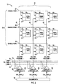
- FIG. 1 is a schematic diagram of a first embodiment of a light modulator array 10 controlled in accordance with the invention. While this example shows a simple light modulator array 10 having only nine pixel cells 20 in a 3 X 3 square array, it will be understood that a light modulator array will have many pixel cells arranged in a convenient configuration such as a rectangular array in which each pixel cell is addressed by a row 30 and a column 40.
- Row 1 is identified by reference numeral 31
- Row 2 by reference numeral 32 Row 3 by reference numeral 33
- Column 1 is identified by reference numeral 41, Column 2 by reference numeral 42, and Column 3 by reference numeral 43.
- Each pixel cell 20 has a V in input 21 and an ENABLE input 22.
- a number of voltage control devices 50 generate a range of analog voltages that are wired to each column voltage select block.
- voltage control devices 50 are digital-to-analog converters (DAC's) 51, 52, and 53.
- the column data 60 for the array controls the voltage select bus for each column.
- the number of bits of digital signal required at the inputs of the DAC's 51 - 53 is determined by the number of different analog voltages desired.
- the row data for the array is similar to that of a conventional binary-driven array. The row data acts as an ENABLE signal for driving the selected column voltage for the selected modulator pixel cell 20 .
- FIG. 2 is a schematic diagram of a second embodiment 15 of a light modulator array controlled in accordance with the invention.
- Rows 1-3 are again identified by reference numerals 31 - 33, and Columns 1-3 are again identified by reference numerals 41- 43 respectively.
- each pixel cell 20 has a voltage V in input 21 and an ENABLE input 22.
- a number of discrete analog reference voltages 70 are provided, such as Vref 1 71, Vref 2 72, and Vref 3 73.
- a set of analog multiplexers (MUX's) 80 select an analog reference voltage for each column, in accordance with column data 60.
- analog MUX 81 selects an analog voltage from among Vref 1 71, Vref 2 72, and Vref 3 73 to apply to the Column 1 bus 41.
- analog MUX 82 selects an analog voltage from the same set of analog reference voltages to apply to the Column 2 bus 42
- analog MUX 83 selects an analog voltage from the same set of analog reference voltages to apply to the Column 3 bus 43.
- the row data acts as an ENABLE signal for driving the selected column voltage V in for the selected modulator pixel cell 20.
- Programmable analog reference voltages 70 such as Vref 1 71, Vref 2 72, and Vref 3 73 may be generated by a single set of conventional DAC's (not shown) for the whole light modulator array 15, using a DAC for each of the discrete analog reference voltages 71- 73.
- DAC's not shown
- the number of discrete analog reference voltages is not limited to the three illustrated in FIG. 2 and that any desired number of discrete analog reference voltages may be employed.
- FIG. 3 shows, in a simple schematic block diagram, drive circuitry for a voltage-driven MEMS element such as a light-modulation pixel element, illustrating how voltage V in input 21 and ENABLE input 22 are implemented at each pixel cell 20.
- a single pass gate 90 gated by a row ENABLE signal 35 drives the selected V in voltage input 45 to be applied to the modulator pixel cell 20.
- a capacitor 25 may be used to hold the applied analog voltage V in if needed, or pixel cell 20 may have a built-in capacitance C, obviating the need for a separate capacitor 25 .
- both of the embodiments of FIGS. 1 and 2 utilize a number of voltage control elements 50 or 80 respectively to generate a desired range of discrete analog voltages.
- the discrete analog voltages are then multiplexed onto the column lines of the modulator array. Multiplexing any one of a given range of voltages to an individual pixel cell, as opposed to generating an analog voltage level at each cell, enables improved color resolution with a minimal increase in data rates.
- any one of a given range of voltages to an individual pixel cell can also eliminate the need for more expensive fabrication processes and allow analog control circuitry of a size that can fit under individual pixel elements of the modulator array.
- the methods described for controlling both light modulator arrays 10 and 15 include providing a number of discrete analog voltages.
- the methods described use row lines 30 and column lines 40 for each pixel cell 20 of the array by selecting from the discrete voltages a voltage to be applied to the pixel, applying the selected voltage to the column line, and enabling application of the selected voltage to the pixel by selecting the row line for the pixel.
- the discrete voltages provided are analog reference voltages that may be programmed using DAC's, either at each column as in FIG. 1, or for the whole array (or any desired portion of the array) as in FIG. 2.
- the voltage selection, voltage application, and enabling may be performed substantially simultaneously for all pixels of the light modulator array.
- the methods described herein are also applicable for controlling a light modulator array having pixel modulation elements 20 adapted to be responsive to analog voltage signals.
- One provides a number of row lines 30 and a number of column lines 40, each combination of a particular column line and a particular row line being adapted to select a pixel modulation element of the array, and a number of discrete analog voltages 70.
- a voltage to be applied to the pixel is selected from among the discrete analog voltages 70.
- the selected voltage is applied to the column line of the pixel, and application of the selected voltage to the pixel is enabled by selecting the row line for the pixel.
- the selected voltage is applied to the row line of the pixel, and application of the selected voltage to the pixel is enabled by selecting the column line for the pixel.
- the voltage selection, the voltage application, and the enabling may be performed for all pixels of the light modulator array substantially simultaneously.
- each discrete voltage may correspond to a gray level or to a unique combination of hue, saturation, and intensity of color, for example.
- the apparatus includes a number of discrete voltage sources, a multiplexer 80 responsive to the input signal for multiplexing from the discrete voltage sources a selected voltage to be applied to each pixel of the array, and one or more gates 90 for enabling application of the selected discrete voltage to each pixel cell 20 of the array.
- Each discrete voltage source may be a digital-to-analog converter (DAC). If necessary to hold a charge corresponding to the selected analog voltage, the apparatus may include a capacitor 25 coupled to gate 90. Gate 90 may be controlled by a row line 30 or alternatively by a column line 40.
- each voltage select block being coupled to a column line 40 if a row line 30 controls gate 90 , or alternatively to a row line 30 if a column line 30 controls gate 90 .
- the invention provides methods and apparatus for controlling a light-modulator array having a plurality of pixels.
- the controller apparatus provides a number of discrete analog voltages, selects from among the discrete analog voltages a particular analog voltage to be applied to each pixel, and applies the selected analog voltage to each selected pixel. Gating the application of the selected analog voltage to each pixel is also provided by the apparatus. Multiplexing of the analog voltages is integrated with row/column addressing of the light-modulator array.
- the methods and apparatus of the invention are useful for control of many kinds of analog-controllable MEMS device arrays, light modulator arrays and light projectors, such as micro-mirrors, diffraction-based modulators or interference-based modulators, and for control of liquid-crystal (LCD) modulators.
- analog-controllable MEMS device arrays such as micro-mirrors, diffraction-based modulators or interference-based modulators, and for control of liquid-crystal (LCD) modulators.
- LCD liquid-crystal
- the voltage control described may also be used in conjunction with conventional pulse-width modulation, enabling improved color resolution with a minimal increase in required data rate. For example, if two analog voltages are used (e.g., 1 V and 2 V), and two bits of pulse-width data are used (four possible duty cycles), then eight levels of intensity can be achieved.
Landscapes
- Engineering & Computer Science (AREA)
- Physics & Mathematics (AREA)
- Computer Hardware Design (AREA)
- General Physics & Mathematics (AREA)
- Theoretical Computer Science (AREA)
- Mechanical Light Control Or Optical Switches (AREA)
- Control Of Indicators Other Than Cathode Ray Tubes (AREA)
- Optical Communication System (AREA)
- Liquid Crystal (AREA)
- Liquid Crystal Display Device Control (AREA)
Abstract
Description
The methods described herein are also applicable for controlling a light modulator array having
Also, those skilled in the art will recognize that the voltage control described may also be used in conjunction with conventional pulse-width modulation, enabling improved color resolution with a minimal increase in required data rate. For example, if two analog voltages are used (e.g., 1 V and 2 V), and two bits of pulse-width data are used (four possible duty cycles), then eight levels of intensity can be achieved.
Claims (10)
- A method for controlling, in response to an input signal, an array of MEMS devices of the type having column lines and row lines for selecting a particular MEMS device of the array, the method comprising the steps of:a) providing a number of discrete voltages; andb) responsive to the input signal, multiplexing from the discrete voltages a selected discrete voltage to be applied to each MEMS device of the array; andc) enabling application of the selected discrete voltage to each MEMS device of the array.
- The method of claim 1, wherein the discrete voltages are analog reference voltages.
- The method of claim 1, wherein each MEMS device of the array comprises a pixel cell of a light modulator.
- A method for controlling, in response to an input signal, a light modulator array of the type having column lines and row lines for selecting a pixel of the array, the method comprising the steps of:a) providing a number of discrete analog voltages; andb) responsive to the input signal, multiplexing from the discrete analog voltages a selected discrete analog voltage to be applied to each pixel of the array; andc) enabling application of the selected discrete analog voltage to each pixel of the array.
- A method for controlling a light modulator array having pixel modulation elements adapted to be responsive to analog voltage signals, the method comprising the steps of:a) providing a number of column lines and a number of row lines, each combination of a column line and a row line being adapted to select a pixel;b) providing a number of discrete voltages; and for each pixel of the array,c) selecting from the discrete voltages a voltage to be applied to the pixel;d) applying the selected voltage to the column line of the pixel; ande) enabling application of the selected voltage to the pixel by selecting the row line for the pixel.
- Apparatus for controlling, in response to an input signal, a light modulator array of the type having column lines and row lines for selecting a pixel of the array, the apparatus comprising:a) a number of discrete voltage sources;b) a multiplexer responsive to the input signal for multiplexing from the discrete voltage sources a selected voltage to be applied to each pixel of the array, the multiplexer comprising a plurality of voltage select blocks, each voltage select block being coupled to a column line; andc) a plurality of gates for enabling application of the selected discrete voltage to each pixel of the array, each gate being coupled to a row line.
- Apparatus for controlling, in response to an input signal, a light modulator array of the type having column lines and row lines for selecting a pixel of the array, the apparatus comprising:a) a number of discrete voltage sources;b) a multiplexer responsive to the input signal for multiplexing from the discrete voltage sources a selected voltage to be applied to each pixel of the array, the multiplexer comprising a plurality of voltage select blocks, each voltage select block being coupled to a row line; andc) a plurality of gates for enabling application of the selected discrete voltage to each pixel of the array, each gate being coupled to a column line.
- A controller for a light-modulator array having a plurality of MEMS devices, the controller comprising:a) means for providing a number of discrete analog voltages;b) means for selecting from the discrete voltages an analog voltage to be applied to each MEMS device; andc) means for applying the selected analog voltage to each MEMS device.
- The controller of claim 8, further comprising:d) means for gating application of the selected analog voltage to each MEMS device.
- The controller of claim 8, wherein each MEMS device of the array comprises a pixel cell of a light modulator.
Applications Claiming Priority (2)
| Application Number | Priority Date | Filing Date | Title |
|---|---|---|---|
| US429144 | 2003-04-30 | ||
| US10/429,144 US6741384B1 (en) | 2003-04-30 | 2003-04-30 | Control of MEMS and light modulator arrays |
Publications (2)
| Publication Number | Publication Date |
|---|---|
| EP1473692A2 true EP1473692A2 (en) | 2004-11-03 |
| EP1473692A3 EP1473692A3 (en) | 2005-03-23 |
Family
ID=32313144
Family Applications (1)
| Application Number | Title | Priority Date | Filing Date |
|---|---|---|---|
| EP04252177A Withdrawn EP1473692A3 (en) | 2003-04-30 | 2004-04-14 | Control of mems and light modulator arrays |
Country Status (6)
| Country | Link |
|---|---|
| US (1) | US6741384B1 (en) |
| EP (1) | EP1473692A3 (en) |
| JP (1) | JP2004334208A (en) |
| KR (1) | KR20040094279A (en) |
| CN (1) | CN1542499A (en) |
| TW (1) | TW200422253A (en) |
Families Citing this family (222)
| Publication number | Priority date | Publication date | Assignee | Title |
|---|---|---|---|---|
| US6674562B1 (en) | 1994-05-05 | 2004-01-06 | Iridigm Display Corporation | Interferometric modulation of radiation |
| US8014059B2 (en) | 1994-05-05 | 2011-09-06 | Qualcomm Mems Technologies, Inc. | System and method for charge control in a MEMS device |
| US7297471B1 (en) | 2003-04-15 | 2007-11-20 | Idc, Llc | Method for manufacturing an array of interferometric modulators |
| US7550794B2 (en) | 2002-09-20 | 2009-06-23 | Idc, Llc | Micromechanical systems device comprising a displaceable electrode and a charge-trapping layer |
| US6680792B2 (en) | 1994-05-05 | 2004-01-20 | Iridigm Display Corporation | Interferometric modulation of radiation |
| US7138984B1 (en) | 2001-06-05 | 2006-11-21 | Idc, Llc | Directly laminated touch sensitive screen |
| US7460291B2 (en) | 1994-05-05 | 2008-12-02 | Idc, Llc | Separable modulator |
| US7123216B1 (en) | 1994-05-05 | 2006-10-17 | Idc, Llc | Photonic MEMS and structures |
| US7471444B2 (en) | 1996-12-19 | 2008-12-30 | Idc, Llc | Interferometric modulation of radiation |
| US7532377B2 (en) | 1998-04-08 | 2009-05-12 | Idc, Llc | Movable micro-electromechanical device |
| US8928967B2 (en) | 1998-04-08 | 2015-01-06 | Qualcomm Mems Technologies, Inc. | Method and device for modulating light |
| WO1999052006A2 (en) | 1998-04-08 | 1999-10-14 | Etalon, Inc. | Interferometric modulation of radiation |
| WO2003007049A1 (en) | 1999-10-05 | 2003-01-23 | Iridigm Display Corporation | Photonic mems and structures |
| US6962771B1 (en) * | 2000-10-13 | 2005-11-08 | Taiwan Semiconductor Manufacturing Company, Ltd. | Dual damascene process |
| US6794119B2 (en) | 2002-02-12 | 2004-09-21 | Iridigm Display Corporation | Method for fabricating a structure for a microelectromechanical systems (MEMS) device |
| US7781850B2 (en) | 2002-09-20 | 2010-08-24 | Qualcomm Mems Technologies, Inc. | Controlling electromechanical behavior of structures within a microelectromechanical systems device |
| US6972881B1 (en) * | 2002-11-21 | 2005-12-06 | Nuelight Corp. | Micro-electro-mechanical switch (MEMS) display panel with on-glass column multiplexers using MEMS as mux elements |
| TW200413810A (en) | 2003-01-29 | 2004-08-01 | Prime View Int Co Ltd | Light interference display panel and its manufacturing method |
| TW594360B (en) | 2003-04-21 | 2004-06-21 | Prime View Int Corp Ltd | A method for fabricating an interference display cell |
| TW570896B (en) | 2003-05-26 | 2004-01-11 | Prime View Int Co Ltd | A method for fabricating an interference display cell |
| US7221495B2 (en) | 2003-06-24 | 2007-05-22 | Idc Llc | Thin film precursor stack for MEMS manufacturing |
| US6856449B2 (en) * | 2003-07-10 | 2005-02-15 | Evans & Sutherland Computer Corporation | Ultra-high resolution light modulation control system and method |
| TWI231865B (en) | 2003-08-26 | 2005-05-01 | Prime View Int Co Ltd | An interference display cell and fabrication method thereof |
| TW593126B (en) | 2003-09-30 | 2004-06-21 | Prime View Int Co Ltd | A structure of a micro electro mechanical system and manufacturing the same |
| US7012726B1 (en) | 2003-11-03 | 2006-03-14 | Idc, Llc | MEMS devices with unreleased thin film components |
| US7161728B2 (en) * | 2003-12-09 | 2007-01-09 | Idc, Llc | Area array modulation and lead reduction in interferometric modulators |
| US7142346B2 (en) | 2003-12-09 | 2006-11-28 | Idc, Llc | System and method for addressing a MEMS display |
| US7532194B2 (en) | 2004-02-03 | 2009-05-12 | Idc, Llc | Driver voltage adjuster |
| US7330297B2 (en) * | 2005-03-04 | 2008-02-12 | Angstrom, Inc | Fine control of rotation and translation of discretely controlled micromirror |
| US7382516B2 (en) * | 2004-06-18 | 2008-06-03 | Angstrom, Inc. | Discretely controlled micromirror with multi-level positions |
| US7898144B2 (en) * | 2006-02-04 | 2011-03-01 | Angstrom, Inc. | Multi-step microactuator providing multi-step displacement to a controlled object |
| US7474454B2 (en) * | 2004-06-18 | 2009-01-06 | Angstrom, Inc. | Programmable micromirror motion control system |
| US7580178B2 (en) * | 2004-02-13 | 2009-08-25 | Angstrom, Inc. | Image-guided microsurgery system and method |
| US7350922B2 (en) * | 2004-02-13 | 2008-04-01 | Angstrom, Inc. | Three-dimensional display using variable focal length micromirror array lens |
| US8537204B2 (en) * | 2004-07-08 | 2013-09-17 | Gyoung Il Cho | 3D television broadcasting system |
| US7751694B2 (en) * | 2004-02-13 | 2010-07-06 | Angstrom, Inc. | Three-dimensional endoscope imaging and display system |
| US7119945B2 (en) | 2004-03-03 | 2006-10-10 | Idc, Llc | Altering temporal response of microelectromechanical elements |
| US7706050B2 (en) | 2004-03-05 | 2010-04-27 | Qualcomm Mems Technologies, Inc. | Integrated modulator illumination |
| US7339746B2 (en) * | 2004-03-22 | 2008-03-04 | Angstrom, Inc. | Small and fast zoom system using micromirror array lens |
| US7410266B2 (en) * | 2004-03-22 | 2008-08-12 | Angstrom, Inc. | Three-dimensional imaging system for robot vision |
| US7768571B2 (en) * | 2004-03-22 | 2010-08-03 | Angstrom, Inc. | Optical tracking system using variable focal length lens |
| US7742232B2 (en) * | 2004-04-12 | 2010-06-22 | Angstrom, Inc. | Three-dimensional imaging system |
| US8049776B2 (en) * | 2004-04-12 | 2011-11-01 | Angstrom, Inc. | Three-dimensional camcorder |
| US7619614B2 (en) * | 2004-04-12 | 2009-11-17 | Angstrom, Inc. | Three-dimensional optical mouse system |
| US20070040924A1 (en) * | 2005-08-19 | 2007-02-22 | Stereo Display, Inc. | Cellular phone camera with three-dimensional imaging function |
| US20070115261A1 (en) * | 2005-11-23 | 2007-05-24 | Stereo Display, Inc. | Virtual Keyboard input system using three-dimensional motion detection by variable focal length lens |
| US7476327B2 (en) | 2004-05-04 | 2009-01-13 | Idc, Llc | Method of manufacture for microelectromechanical devices |
| US7060895B2 (en) * | 2004-05-04 | 2006-06-13 | Idc, Llc | Modifying the electro-mechanical behavior of devices |
| US7164520B2 (en) | 2004-05-12 | 2007-01-16 | Idc, Llc | Packaging for an interferometric modulator |
| US7667896B2 (en) | 2004-05-27 | 2010-02-23 | Angstrom, Inc. | DVD recording and reproducing system |
| US7354167B2 (en) | 2004-05-27 | 2008-04-08 | Angstrom, Inc. | Beam focusing and scanning system using micromirror array lens |
| US7019886B2 (en) * | 2004-05-27 | 2006-03-28 | Hewlett-Packard Development Company, L.P. | Light modulator |
| US7777959B2 (en) * | 2004-05-27 | 2010-08-17 | Angstrom, Inc. | Micromirror array lens with fixed focal length |
| US6970031B1 (en) | 2004-05-28 | 2005-11-29 | Hewlett-Packard Development Company, L.P. | Method and apparatus for reducing charge injection in control of MEMS electrostatic actuator array |
| US7256922B2 (en) | 2004-07-02 | 2007-08-14 | Idc, Llc | Interferometric modulators with thin film transistors |
| WO2006014929A1 (en) | 2004-07-29 | 2006-02-09 | Idc, Llc | System and method for micro-electromechanical operating of an interferometric modulator |
| US7515147B2 (en) | 2004-08-27 | 2009-04-07 | Idc, Llc | Staggered column drive circuit systems and methods |
| US7499208B2 (en) | 2004-08-27 | 2009-03-03 | Udc, Llc | Current mode display driver circuit realization feature |
| US7551159B2 (en) | 2004-08-27 | 2009-06-23 | Idc, Llc | System and method of sensing actuation and release voltages of an interferometric modulator |
| US7889163B2 (en) * | 2004-08-27 | 2011-02-15 | Qualcomm Mems Technologies, Inc. | Drive method for MEMS devices |
| US7560299B2 (en) | 2004-08-27 | 2009-07-14 | Idc, Llc | Systems and methods of actuating MEMS display elements |
| US7602375B2 (en) * | 2004-09-27 | 2009-10-13 | Idc, Llc | Method and system for writing data to MEMS display elements |
| US7373026B2 (en) | 2004-09-27 | 2008-05-13 | Idc, Llc | MEMS device fabricated on a pre-patterned substrate |
| US7684104B2 (en) | 2004-09-27 | 2010-03-23 | Idc, Llc | MEMS using filler material and method |
| US7302157B2 (en) | 2004-09-27 | 2007-11-27 | Idc, Llc | System and method for multi-level brightness in interferometric modulation |
| US7405924B2 (en) | 2004-09-27 | 2008-07-29 | Idc, Llc | System and method for protecting microelectromechanical systems array using structurally reinforced back-plate |
| US7321456B2 (en) | 2004-09-27 | 2008-01-22 | Idc, Llc | Method and device for corner interferometric modulation |
| US7349136B2 (en) | 2004-09-27 | 2008-03-25 | Idc, Llc | Method and device for a display having transparent components integrated therein |
| US7429334B2 (en) | 2004-09-27 | 2008-09-30 | Idc, Llc | Methods of fabricating interferometric modulators by selectively removing a material |
| US7843410B2 (en) | 2004-09-27 | 2010-11-30 | Qualcomm Mems Technologies, Inc. | Method and device for electrically programmable display |
| US7355780B2 (en) | 2004-09-27 | 2008-04-08 | Idc, Llc | System and method of illuminating interferometric modulators using backlighting |
| US7130104B2 (en) | 2004-09-27 | 2006-10-31 | Idc, Llc | Methods and devices for inhibiting tilting of a mirror in an interferometric modulator |
| US7424198B2 (en) | 2004-09-27 | 2008-09-09 | Idc, Llc | Method and device for packaging a substrate |
| US20060076634A1 (en) | 2004-09-27 | 2006-04-13 | Lauren Palmateer | Method and system for packaging MEMS devices with incorporated getter |
| US7626581B2 (en) | 2004-09-27 | 2009-12-01 | Idc, Llc | Device and method for display memory using manipulation of mechanical response |
| US20060176487A1 (en) | 2004-09-27 | 2006-08-10 | William Cummings | Process control monitors for interferometric modulators |
| US7936497B2 (en) | 2004-09-27 | 2011-05-03 | Qualcomm Mems Technologies, Inc. | MEMS device having deformable membrane characterized by mechanical persistence |
| US7630119B2 (en) | 2004-09-27 | 2009-12-08 | Qualcomm Mems Technologies, Inc. | Apparatus and method for reducing slippage between structures in an interferometric modulator |
| US7553684B2 (en) | 2004-09-27 | 2009-06-30 | Idc, Llc | Method of fabricating interferometric devices using lift-off processing techniques |
| US7583429B2 (en) | 2004-09-27 | 2009-09-01 | Idc, Llc | Ornamental display device |
| US7304784B2 (en) | 2004-09-27 | 2007-12-04 | Idc, Llc | Reflective display device having viewable display on both sides |
| US8008736B2 (en) | 2004-09-27 | 2011-08-30 | Qualcomm Mems Technologies, Inc. | Analog interferometric modulator device |
| US7554714B2 (en) | 2004-09-27 | 2009-06-30 | Idc, Llc | Device and method for manipulation of thermal response in a modulator |
| US7289259B2 (en) | 2004-09-27 | 2007-10-30 | Idc, Llc | Conductive bus structure for interferometric modulator array |
| US7692839B2 (en) | 2004-09-27 | 2010-04-06 | Qualcomm Mems Technologies, Inc. | System and method of providing MEMS device with anti-stiction coating |
| US7417735B2 (en) | 2004-09-27 | 2008-08-26 | Idc, Llc | Systems and methods for measuring color and contrast in specular reflective devices |
| US7679627B2 (en) | 2004-09-27 | 2010-03-16 | Qualcomm Mems Technologies, Inc. | Controller and driver features for bi-stable display |
| US7527995B2 (en) | 2004-09-27 | 2009-05-05 | Qualcomm Mems Technologies, Inc. | Method of making prestructure for MEMS systems |
| CN100439967C (en) * | 2004-09-27 | 2008-12-03 | Idc公司 | Method and apparatus for multi-state interferometric light modulation |
| US7369296B2 (en) | 2004-09-27 | 2008-05-06 | Idc, Llc | Device and method for modifying actuation voltage thresholds of a deformable membrane in an interferometric modulator |
| US7343080B2 (en) | 2004-09-27 | 2008-03-11 | Idc, Llc | System and method of testing humidity in a sealed MEMS device |
| US7161730B2 (en) | 2004-09-27 | 2007-01-09 | Idc, Llc | System and method for providing thermal compensation for an interferometric modulator display |
| US7405861B2 (en) | 2004-09-27 | 2008-07-29 | Idc, Llc | Method and device for protecting interferometric modulators from electrostatic discharge |
| US7359066B2 (en) | 2004-09-27 | 2008-04-15 | Idc, Llc | Electro-optical measurement of hysteresis in interferometric modulators |
| US7653371B2 (en) | 2004-09-27 | 2010-01-26 | Qualcomm Mems Technologies, Inc. | Selectable capacitance circuit |
| US7944599B2 (en) | 2004-09-27 | 2011-05-17 | Qualcomm Mems Technologies, Inc. | Electromechanical device with optical function separated from mechanical and electrical function |
| US7808703B2 (en) | 2004-09-27 | 2010-10-05 | Qualcomm Mems Technologies, Inc. | System and method for implementation of interferometric modulator displays |
| US7916103B2 (en) | 2004-09-27 | 2011-03-29 | Qualcomm Mems Technologies, Inc. | System and method for display device with end-of-life phenomena |
| US7668415B2 (en) | 2004-09-27 | 2010-02-23 | Qualcomm Mems Technologies, Inc. | Method and device for providing electronic circuitry on a backplate |
| US7327510B2 (en) | 2004-09-27 | 2008-02-05 | Idc, Llc | Process for modifying offset voltage characteristics of an interferometric modulator |
| US7535466B2 (en) | 2004-09-27 | 2009-05-19 | Idc, Llc | System with server based control of client device display features |
| US7369294B2 (en) | 2004-09-27 | 2008-05-06 | Idc, Llc | Ornamental display device |
| US7345805B2 (en) | 2004-09-27 | 2008-03-18 | Idc, Llc | Interferometric modulator array with integrated MEMS electrical switches |
| US7417783B2 (en) | 2004-09-27 | 2008-08-26 | Idc, Llc | Mirror and mirror layer for optical modulator and method |
| US7372613B2 (en) | 2004-09-27 | 2008-05-13 | Idc, Llc | Method and device for multistate interferometric light modulation |
| US7446927B2 (en) | 2004-09-27 | 2008-11-04 | Idc, Llc | MEMS switch with set and latch electrodes |
| US7289256B2 (en) | 2004-09-27 | 2007-10-30 | Idc, Llc | Electrical characterization of interferometric modulators |
| US7893919B2 (en) | 2004-09-27 | 2011-02-22 | Qualcomm Mems Technologies, Inc. | Display region architectures |
| US7136213B2 (en) | 2004-09-27 | 2006-11-14 | Idc, Llc | Interferometric modulators having charge persistence |
| US7701631B2 (en) | 2004-09-27 | 2010-04-20 | Qualcomm Mems Technologies, Inc. | Device having patterned spacers for backplates and method of making the same |
| US7564612B2 (en) | 2004-09-27 | 2009-07-21 | Idc, Llc | Photonic MEMS and structures |
| US7545550B2 (en) | 2004-09-27 | 2009-06-09 | Idc, Llc | Systems and methods of actuating MEMS display elements |
| US7724993B2 (en) | 2004-09-27 | 2010-05-25 | Qualcomm Mems Technologies, Inc. | MEMS switches with deforming membranes |
| US7310179B2 (en) | 2004-09-27 | 2007-12-18 | Idc, Llc | Method and device for selective adjustment of hysteresis window |
| US7675669B2 (en) | 2004-09-27 | 2010-03-09 | Qualcomm Mems Technologies, Inc. | Method and system for driving interferometric modulators |
| US7259449B2 (en) | 2004-09-27 | 2007-08-21 | Idc, Llc | Method and system for sealing a substrate |
| US8310441B2 (en) | 2004-09-27 | 2012-11-13 | Qualcomm Mems Technologies, Inc. | Method and system for writing data to MEMS display elements |
| US7420725B2 (en) | 2004-09-27 | 2008-09-02 | Idc, Llc | Device having a conductive light absorbing mask and method for fabricating same |
| US8878825B2 (en) | 2004-09-27 | 2014-11-04 | Qualcomm Mems Technologies, Inc. | System and method for providing a variable refresh rate of an interferometric modulator display |
| US7492502B2 (en) | 2004-09-27 | 2009-02-17 | Idc, Llc | Method of fabricating a free-standing microstructure |
| US7415186B2 (en) | 2004-09-27 | 2008-08-19 | Idc, Llc | Methods for visually inspecting interferometric modulators for defects |
| US7453579B2 (en) | 2004-09-27 | 2008-11-18 | Idc, Llc | Measurement of the dynamic characteristics of interferometric modulators |
| US7317568B2 (en) | 2004-09-27 | 2008-01-08 | Idc, Llc | System and method of implementation of interferometric modulators for display mirrors |
| US7710629B2 (en) | 2004-09-27 | 2010-05-04 | Qualcomm Mems Technologies, Inc. | System and method for display device with reinforcing substance |
| US7299681B2 (en) | 2004-09-27 | 2007-11-27 | Idc, Llc | Method and system for detecting leak in electronic devices |
| US7460246B2 (en) | 2004-09-27 | 2008-12-02 | Idc, Llc | Method and system for sensing light using interferometric elements |
| US7813026B2 (en) | 2004-09-27 | 2010-10-12 | Qualcomm Mems Technologies, Inc. | System and method of reducing color shift in a display |
| US7920135B2 (en) | 2004-09-27 | 2011-04-05 | Qualcomm Mems Technologies, Inc. | Method and system for driving a bi-stable display |
| US7586484B2 (en) | 2004-09-27 | 2009-09-08 | Idc, Llc | Controller and driver features for bi-stable display |
| US7368803B2 (en) | 2004-09-27 | 2008-05-06 | Idc, Llc | System and method for protecting microelectromechanical systems array using back-plate with non-flat portion |
| US8124434B2 (en) | 2004-09-27 | 2012-02-28 | Qualcomm Mems Technologies, Inc. | Method and system for packaging a display |
| US7532195B2 (en) | 2004-09-27 | 2009-05-12 | Idc, Llc | Method and system for reducing power consumption in a display |
| US7719500B2 (en) | 2004-09-27 | 2010-05-18 | Qualcomm Mems Technologies, Inc. | Reflective display pixels arranged in non-rectangular arrays |
| US7489434B2 (en) | 2007-05-02 | 2009-02-10 | Angstrom, Inc. | Hybrid micromirror array lens for reducing chromatic aberration |
| US7619807B2 (en) * | 2004-11-08 | 2009-11-17 | Angstrom, Inc. | Micromirror array lens with optical surface profiles |
| TW200628877A (en) | 2005-02-04 | 2006-08-16 | Prime View Int Co Ltd | Method of manufacturing optical interference type color display |
| EP2116885B1 (en) * | 2005-02-23 | 2014-07-23 | Pixtronix, Inc. | Display methods and apparatus |
| US9158106B2 (en) | 2005-02-23 | 2015-10-13 | Pixtronix, Inc. | Display methods and apparatus |
| US8159428B2 (en) | 2005-02-23 | 2012-04-17 | Pixtronix, Inc. | Display methods and apparatus |
| US8310442B2 (en) | 2005-02-23 | 2012-11-13 | Pixtronix, Inc. | Circuits for controlling display apparatus |
| US9261694B2 (en) | 2005-02-23 | 2016-02-16 | Pixtronix, Inc. | Display apparatus and methods for manufacture thereof |
| CN101256279B (en) * | 2005-02-23 | 2014-04-02 | 皮克斯特隆尼斯有限公司 | Display method and apparatus |
| US9229222B2 (en) | 2005-02-23 | 2016-01-05 | Pixtronix, Inc. | Alignment methods in fluid-filled MEMS displays |
| US8482496B2 (en) | 2006-01-06 | 2013-07-09 | Pixtronix, Inc. | Circuits for controlling MEMS display apparatus on a transparent substrate |
| US9082353B2 (en) | 2010-01-05 | 2015-07-14 | Pixtronix, Inc. | Circuits for controlling display apparatus |
| US20070205969A1 (en) | 2005-02-23 | 2007-09-06 | Pixtronix, Incorporated | Direct-view MEMS display devices and methods for generating images thereon |
| US8519945B2 (en) | 2006-01-06 | 2013-08-27 | Pixtronix, Inc. | Circuits for controlling display apparatus |
| US7999994B2 (en) | 2005-02-23 | 2011-08-16 | Pixtronix, Inc. | Display apparatus and methods for manufacture thereof |
| US20060198011A1 (en) * | 2005-03-04 | 2006-09-07 | Stereo Display, Inc. | Volumetric three-dimensional device using two-dimensional scanning device |
| US20060203117A1 (en) * | 2005-03-10 | 2006-09-14 | Stereo Display, Inc. | Video monitoring system using variable focal length lens |
| US7920136B2 (en) | 2005-05-05 | 2011-04-05 | Qualcomm Mems Technologies, Inc. | System and method of driving a MEMS display device |
| US7948457B2 (en) | 2005-05-05 | 2011-05-24 | Qualcomm Mems Technologies, Inc. | Systems and methods of actuating MEMS display elements |
| CA2607807A1 (en) | 2005-05-05 | 2006-11-16 | Qualcomm Incorporated | Dynamic driver ic and display panel configuration |
| US7321416B2 (en) * | 2005-06-15 | 2008-01-22 | Asml Netherlands B.V. | Lithographic apparatus, device manufacturing method, device manufactured thereby, and controllable patterning device utilizing a spatial light modulator with distributed digital to analog conversion |
| JP2009503564A (en) | 2005-07-22 | 2009-01-29 | クアルコム,インコーポレイテッド | Support structure for MEMS device and method thereof |
| US20070041077A1 (en) * | 2005-08-19 | 2007-02-22 | Stereo Display, Inc. | Pocket-sized two-dimensional image projection system |
| US20070052671A1 (en) * | 2005-09-02 | 2007-03-08 | Hewlett-Packard Development Company Lp | Pixel element actuation |
| US7355779B2 (en) | 2005-09-02 | 2008-04-08 | Idc, Llc | Method and system for driving MEMS display elements |
| US7630114B2 (en) | 2005-10-28 | 2009-12-08 | Idc, Llc | Diffusion barrier layer for MEMS devices |
| US8391630B2 (en) | 2005-12-22 | 2013-03-05 | Qualcomm Mems Technologies, Inc. | System and method for power reduction when decompressing video streams for interferometric modulator displays |
| US7795061B2 (en) | 2005-12-29 | 2010-09-14 | Qualcomm Mems Technologies, Inc. | Method of creating MEMS device cavities by a non-etching process |
| US7636151B2 (en) | 2006-01-06 | 2009-12-22 | Qualcomm Mems Technologies, Inc. | System and method for providing residual stress test structures |
| US7916980B2 (en) | 2006-01-13 | 2011-03-29 | Qualcomm Mems Technologies, Inc. | Interconnect structure for MEMS device |
| US7382515B2 (en) | 2006-01-18 | 2008-06-03 | Qualcomm Mems Technologies, Inc. | Silicon-rich silicon nitrides as etch stops in MEMS manufacture |
| US8194056B2 (en) | 2006-02-09 | 2012-06-05 | Qualcomm Mems Technologies Inc. | Method and system for writing data to MEMS display elements |
| US7582952B2 (en) | 2006-02-21 | 2009-09-01 | Qualcomm Mems Technologies, Inc. | Method for providing and removing discharging interconnect for chip-on-glass output leads and structures thereof |
| US7547568B2 (en) | 2006-02-22 | 2009-06-16 | Qualcomm Mems Technologies, Inc. | Electrical conditioning of MEMS device and insulating layer thereof |
| US8526096B2 (en) | 2006-02-23 | 2013-09-03 | Pixtronix, Inc. | Mechanical light modulators with stressed beams |
| US7550810B2 (en) | 2006-02-23 | 2009-06-23 | Qualcomm Mems Technologies, Inc. | MEMS device having a layer movable at asymmetric rates |
| US7450295B2 (en) | 2006-03-02 | 2008-11-11 | Qualcomm Mems Technologies, Inc. | Methods for producing MEMS with protective coatings using multi-component sacrificial layers |
| US7643203B2 (en) | 2006-04-10 | 2010-01-05 | Qualcomm Mems Technologies, Inc. | Interferometric optical display system with broadband characteristics |
| US7903047B2 (en) | 2006-04-17 | 2011-03-08 | Qualcomm Mems Technologies, Inc. | Mode indicator for interferometric modulator displays |
| US7623287B2 (en) | 2006-04-19 | 2009-11-24 | Qualcomm Mems Technologies, Inc. | Non-planar surface structures and process for microelectromechanical systems |
| US7711239B2 (en) | 2006-04-19 | 2010-05-04 | Qualcomm Mems Technologies, Inc. | Microelectromechanical device and method utilizing nanoparticles |
| US7417784B2 (en) | 2006-04-19 | 2008-08-26 | Qualcomm Mems Technologies, Inc. | Microelectromechanical device and method utilizing a porous surface |
| US7527996B2 (en) | 2006-04-19 | 2009-05-05 | Qualcomm Mems Technologies, Inc. | Non-planar surface structures and process for microelectromechanical systems |
| US8049713B2 (en) | 2006-04-24 | 2011-11-01 | Qualcomm Mems Technologies, Inc. | Power consumption optimized display update |
| US7369292B2 (en) | 2006-05-03 | 2008-05-06 | Qualcomm Mems Technologies, Inc. | Electrode and interconnect materials for MEMS devices |
| US9736346B2 (en) | 2006-05-09 | 2017-08-15 | Stereo Display, Inc | Imaging system improving image resolution of the system with low resolution image sensor |
| US7321457B2 (en) | 2006-06-01 | 2008-01-22 | Qualcomm Incorporated | Process and structure for fabrication of MEMS device having isolated edge posts |
| US7649671B2 (en) | 2006-06-01 | 2010-01-19 | Qualcomm Mems Technologies, Inc. | Analog interferometric modulator device with electrostatic actuation and release |
| US7405863B2 (en) | 2006-06-01 | 2008-07-29 | Qualcomm Mems Technologies, Inc. | Patterning of mechanical layer in MEMS to reduce stresses at supports |
| US7471442B2 (en) | 2006-06-15 | 2008-12-30 | Qualcomm Mems Technologies, Inc. | Method and apparatus for low range bit depth enhancements for MEMS display architectures |
| US7702192B2 (en) | 2006-06-21 | 2010-04-20 | Qualcomm Mems Technologies, Inc. | Systems and methods for driving MEMS display |
| US7835061B2 (en) | 2006-06-28 | 2010-11-16 | Qualcomm Mems Technologies, Inc. | Support structures for free-standing electromechanical devices |
| US7385744B2 (en) | 2006-06-28 | 2008-06-10 | Qualcomm Mems Technologies, Inc. | Support structure for free-standing MEMS device and methods for forming the same |
| US7777715B2 (en) * | 2006-06-29 | 2010-08-17 | Qualcomm Mems Technologies, Inc. | Passive circuits for de-multiplexing display inputs |
| US7388704B2 (en) | 2006-06-30 | 2008-06-17 | Qualcomm Mems Technologies, Inc. | Determination of interferometric modulator mirror curvature and airgap variation using digital photographs |
| US7527998B2 (en) | 2006-06-30 | 2009-05-05 | Qualcomm Mems Technologies, Inc. | Method of manufacturing MEMS devices providing air gap control |
| US7763546B2 (en) | 2006-08-02 | 2010-07-27 | Qualcomm Mems Technologies, Inc. | Methods for reducing surface charges during the manufacture of microelectromechanical systems devices |
| US7566664B2 (en) | 2006-08-02 | 2009-07-28 | Qualcomm Mems Technologies, Inc. | Selective etching of MEMS using gaseous halides and reactive co-etchants |
| US7365899B2 (en) * | 2006-08-10 | 2008-04-29 | Angstrom, Inc. | Micromirror with multi-axis rotation and translation |
| US7589884B2 (en) * | 2006-09-22 | 2009-09-15 | Angstrom, Inc. | Micromirror array lens with encapsulation of reflective metal layer and method of making the same |
| US7589885B2 (en) * | 2006-09-22 | 2009-09-15 | Angstrom, Inc. | Micromirror array device comprising encapsulated reflective metal layer and method of making the same |
| US7891818B2 (en) | 2006-12-12 | 2011-02-22 | Evans & Sutherland Computer Corporation | System and method for aligning RGB light in a single modulator projector |
| US7488082B2 (en) | 2006-12-12 | 2009-02-10 | Angstrom, Inc. | Discretely controlled micromirror array device with segmented electrodes |
| US9176318B2 (en) | 2007-05-18 | 2015-11-03 | Pixtronix, Inc. | Methods for manufacturing fluid-filled MEMS displays |
| US7403180B1 (en) * | 2007-01-29 | 2008-07-22 | Qualcomm Mems Technologies, Inc. | Hybrid color synthesis for multistate reflective modulator displays |
| US7535618B2 (en) * | 2007-03-12 | 2009-05-19 | Angstrom, Inc. | Discretely controlled micromirror device having multiple motions |
| US7719752B2 (en) | 2007-05-11 | 2010-05-18 | Qualcomm Mems Technologies, Inc. | MEMS structures, methods of fabricating MEMS components on separate substrates and assembly of same |
| US9505606B2 (en) * | 2007-06-13 | 2016-11-29 | Angstrom, Inc. | MEMS actuator with discretely controlled multiple motions |
| US7605988B2 (en) * | 2007-07-23 | 2009-10-20 | Angstrom, Inc. | Compact image taking lens system with a lens-surfaced prism |
| US7589916B2 (en) * | 2007-08-10 | 2009-09-15 | Angstrom, Inc. | Micromirror array with iris function |
| US20090185067A1 (en) * | 2007-12-21 | 2009-07-23 | Stereo Display, Inc. | Compact automatic focusing camera |
| US8451298B2 (en) * | 2008-02-13 | 2013-05-28 | Qualcomm Mems Technologies, Inc. | Multi-level stochastic dithering with noise mitigation via sequential template averaging |
| US8810908B2 (en) * | 2008-03-18 | 2014-08-19 | Stereo Display, Inc. | Binoculars with micromirror array lenses |
| US20090303569A1 (en) * | 2008-05-20 | 2009-12-10 | Stereo Didplay, Inc. | Self-tilted micromirror device |
| US8622557B2 (en) * | 2008-05-20 | 2014-01-07 | Stereo Display, Inc. | Micromirror array lens with self-tilted micromirrors |
| US8358317B2 (en) | 2008-05-23 | 2013-01-22 | Evans & Sutherland Computer Corporation | System and method for displaying a planar image on a curved surface |
| US8702248B1 (en) | 2008-06-11 | 2014-04-22 | Evans & Sutherland Computer Corporation | Projection method for reducing interpixel gaps on a viewing surface |
| US8169679B2 (en) | 2008-10-27 | 2012-05-01 | Pixtronix, Inc. | MEMS anchors |
| US8077378B1 (en) | 2008-11-12 | 2011-12-13 | Evans & Sutherland Computer Corporation | Calibration system and method for light modulation device |
| US8736590B2 (en) | 2009-03-27 | 2014-05-27 | Qualcomm Mems Technologies, Inc. | Low voltage driver scheme for interferometric modulators |
| WO2010141766A1 (en) * | 2009-06-05 | 2010-12-09 | Qualcomm Mems Technologies, Inc. | System and method for improving the quality of halftone video using a fixed threshold |
| BR112012019383A2 (en) | 2010-02-02 | 2017-09-12 | Pixtronix Inc | CIRCUITS TO CONTROL DISPLAY APPARATUS |
| KR20130100232A (en) | 2010-04-09 | 2013-09-10 | 퀄컴 엠이엠에스 테크놀로지스, 인크. | Mechanical layer of an electromechanical device and methods of forming the same |
| US20110261046A1 (en) * | 2010-04-22 | 2011-10-27 | Qualcomm Mems Technologies, Inc. | System and method for pixel-level voltage boosting |
| US8963159B2 (en) | 2011-04-04 | 2015-02-24 | Qualcomm Mems Technologies, Inc. | Pixel via and methods of forming the same |
| US9134527B2 (en) | 2011-04-04 | 2015-09-15 | Qualcomm Mems Technologies, Inc. | Pixel via and methods of forming the same |
| US9641826B1 (en) | 2011-10-06 | 2017-05-02 | Evans & Sutherland Computer Corporation | System and method for displaying distant 3-D stereo on a dome surface |
| US9175957B2 (en) * | 2012-09-24 | 2015-11-03 | Alces Technology, Inc. | Grayscale patterns from binary spatial light modulators |
| US9134552B2 (en) | 2013-03-13 | 2015-09-15 | Pixtronix, Inc. | Display apparatus with narrow gap electrostatic actuators |
Family Cites Families (9)
| Publication number | Priority date | Publication date | Assignee | Title |
|---|---|---|---|---|
| US4615595A (en) | 1984-10-10 | 1986-10-07 | Texas Instruments Incorporated | Frame addressed spatial light modulator |
| US5835255A (en) | 1986-04-23 | 1998-11-10 | Etalon, Inc. | Visible spectrum modulator arrays |
| US5028939A (en) | 1988-08-23 | 1991-07-02 | Texas Instruments Incorporated | Spatial light modulator system |
| US5254980A (en) | 1991-09-06 | 1993-10-19 | Texas Instruments Incorporated | DMD display system controller |
| US6040937A (en) | 1994-05-05 | 2000-03-21 | Etalon, Inc. | Interferometric modulation |
| KR0149215B1 (en) * | 1994-11-11 | 1998-10-15 | 배순훈 | Pixel driving circuit |
| US5610624A (en) | 1994-11-30 | 1997-03-11 | Texas Instruments Incorporated | Spatial light modulator with reduced possibility of an on state defect |
| US6310591B1 (en) | 1998-08-18 | 2001-10-30 | Texas Instruments Incorporated | Spatial-temporal multiplexing for high bit-depth resolution displays |
| US6985271B2 (en) * | 2002-03-12 | 2006-01-10 | Corning Incorporated | Pointing angle control of electrostatic micro mirrors |
-
2003
- 2003-04-30 US US10/429,144 patent/US6741384B1/en not_active Expired - Lifetime
- 2003-10-29 TW TW092130082A patent/TW200422253A/en unknown
- 2003-12-01 KR KR1020030086413A patent/KR20040094279A/en not_active Withdrawn
-
2004
- 2004-01-30 CN CNA2004100025414A patent/CN1542499A/en active Pending
- 2004-04-14 EP EP04252177A patent/EP1473692A3/en not_active Withdrawn
- 2004-04-30 JP JP2004135640A patent/JP2004334208A/en not_active Withdrawn
Also Published As
| Publication number | Publication date |
|---|---|
| US6741384B1 (en) | 2004-05-25 |
| JP2004334208A (en) | 2004-11-25 |
| CN1542499A (en) | 2004-11-03 |
| TW200422253A (en) | 2004-11-01 |
| EP1473692A3 (en) | 2005-03-23 |
| KR20040094279A (en) | 2004-11-09 |
Similar Documents
| Publication | Publication Date | Title |
|---|---|---|
| US6741384B1 (en) | Control of MEMS and light modulator arrays | |
| US6480177B2 (en) | Blocked stepped address voltage for micromechanical devices | |
| EP0861484B1 (en) | Lcd driver ic with pixel inversion operation | |
| KR100459053B1 (en) | How to remove artifacts from a video display system | |
| EP0689181B1 (en) | Memory schemes for spatial light modulators | |
| US5673060A (en) | Deformable mirror device driving circuit and method | |
| US8228595B2 (en) | Sequence and timing control of writing and rewriting pixel memories with substantially lower data rate | |
| KR930018457A (en) | Multi-gradation dot matrix display method and apparatus | |
| US6525709B1 (en) | Miniature display apparatus and method | |
| KR20010111264A (en) | Signal driver with ramp generator for electro-optic display device | |
| US20040125422A1 (en) | Data driver with gamma correction | |
| JP2004053715A (en) | Display device and its gamma correction method | |
| US6850218B2 (en) | Frame prewriting in a liquid crystal display | |
| US20030107544A1 (en) | Display devices and driving method therefor | |
| JP2004533018A (en) | Addressing an array of display elements | |
| JP2004533018A5 (en) | ||
| US12094387B2 (en) | Offset drive scheme for digital display | |
| US20090167964A1 (en) | Video system including a liquid crystal matrix display with improved addressing method | |
| JPH0460583A (en) | Driving circuit of liquid crystal display device | |
| CN114627824A (en) | Spatial light modulator control | |
| US20020067337A1 (en) | Liquid crystal display imager and clock reduction method | |
| JP2890964B2 (en) | Liquid crystal display | |
| KR19990026585A (en) | Gray voltage generator circuit of liquid crystal display | |
| WO2003090198A1 (en) | System and method for providing voltages for a liquid crystal display | |
| JPH0460584A (en) | Driving circuit of liquid crystal display device |
Legal Events
| Date | Code | Title | Description |
|---|---|---|---|
| PUAI | Public reference made under article 153(3) epc to a published international application that has entered the european phase |
Free format text: ORIGINAL CODE: 0009012 |
|
| AK | Designated contracting states |
Kind code of ref document: A2 Designated state(s): AT BE BG CH CY CZ DE DK EE ES FI FR GB GR HU IE IT LI LU MC NL PL PT RO SE SI SK TR |
|
| AX | Request for extension of the european patent |
Extension state: AL HR LT LV MK |
|
| PUAL | Search report despatched |
Free format text: ORIGINAL CODE: 0009013 |
|
| AK | Designated contracting states |
Kind code of ref document: A3 Designated state(s): AT BE BG CH CY CZ DE DK EE ES FI FR GB GR HU IE IT LI LU MC NL PL PT RO SE SI SK TR |
|
| AX | Request for extension of the european patent |
Extension state: AL HR LT LV MK |
|
| 17P | Request for examination filed |
Effective date: 20050919 |
|
| AKX | Designation fees paid |
Designated state(s): DE FR GB NL |
|
| STAA | Information on the status of an ep patent application or granted ep patent |
Free format text: STATUS: THE APPLICATION IS DEEMED TO BE WITHDRAWN |
|
| 18D | Application deemed to be withdrawn |
Effective date: 20060927 |