EP1473644A2 - Verfahren zur Abbildung eines logischen Schlatkreises auf eine programmierbare Nachschlagetabelle - Google Patents
Verfahren zur Abbildung eines logischen Schlatkreises auf eine programmierbare Nachschlagetabelle Download PDFInfo
- Publication number
- EP1473644A2 EP1473644A2 EP04009701A EP04009701A EP1473644A2 EP 1473644 A2 EP1473644 A2 EP 1473644A2 EP 04009701 A EP04009701 A EP 04009701A EP 04009701 A EP04009701 A EP 04009701A EP 1473644 A2 EP1473644 A2 EP 1473644A2
- Authority
- EP
- European Patent Office
- Prior art keywords
- mapping
- logic element
- logic
- lut
- elements
- Prior art date
- Legal status (The legal status is an assumption and is not a legal conclusion. Google has not performed a legal analysis and makes no representation as to the accuracy of the status listed.)
- Ceased
Links
Images


Classifications
-
- G—PHYSICS
- G06—COMPUTING OR CALCULATING; COUNTING
- G06F—ELECTRIC DIGITAL DATA PROCESSING
- G06F30/00—Computer-aided design [CAD]
- G06F30/30—Circuit design
- G06F30/34—Circuit design for reconfigurable circuits, e.g. field programmable gate arrays [FPGA] or programmable logic devices [PLD]
Definitions
- the present invention relates to Field Programmable Gate Arrays (FPGA) and more particularly, to an improved method for mapping a logic circuit to a programmable look up tables.
- FPGA Field Programmable Gate Arrays
- a programmable logic array device has a plurality of logic elements connected though an interconnect architecture. Electrical circuits are mapped over these logic elements to enable the device to perform desired operations. Mapping of an electrical circuit to an FPGA is a time consuming process hence an technologies emphasizes to increase the speed of the mapping process.
- the important objectives during mapping of an electrical circuit over an FPGA are, to map maximum number of circuit elements over a single logic element and to achieve a smallest possible tree of logic elements to realize the electrical circuit
- Different technology propose different method to achieving said objectives.
- R. J. Francis; J. Rose et. al. [1] proposes a mapping algorithm that reduces delay by using bin packing to determine the gate level decomposition of every node in the network.
- Figure 1 shows a flow diagram of the algorithm.
- the gate level Net-list 1.1 containing information about the logic gates is inserted for mapping onto the LUTs in FPGAs.
- N denotes the given network of logic gates contained in the Net-list
- N t (v) denotes a sub-network generated at a node v
- the next step is to generate sub-network N t (v) at each node v 1.2 of the network N.
- the sub-network N t (v) contains the node v itself along with all the transitive fanins of node v including the primary inputs.
- k-distinct paths are found in the sub-network N t (v) by applying known techniques such as depth first, breadth first search and the like.
- minimum height k-feasible cut is found in the sub-network N t (v) 1.3 starting from v till the primary inputs and LUTs are formed.
- the next step followed in the algorithm is to level each gate of the design 1.4 and subsequently, map the given design starting from the primary output towards the primary inputs 1.5 onto a LUT.
- Figure 2 shows the generation of sub-networks N t (v) using the algorithm discussed above.
- sub-network N t (12) generated at the node 12 starts from node 12 and continues till the primary nodes 1, 2, 3, 4 and 5.
- a four input LUT is formed at node 12 for the sub-network N t (v). Nodes inside the cone are 10, 11 and 12, while the fanin nodes of the cone are 6, 7, 8 and 9.
- J. Cong et.al. [4] have suggested an algorithm for FPGA mapping technology.
- a number of depth relaxation operation are performed to obtain a new network with bounded increase in depth and advantageous to subsequent re-mapping for area minimization by gradually increasing depth bound..
- the Flow-map algorithm described above suffers from a drawback, i.e., the runtime of the algorithm gets increased while constructing sub-networks and finding cut for each node of the circuit. This increase becomes even more prominent when the delay of a circuit increases.
- the object of this invention is to obviate the above drawbacks in the prior art and provide a to a method for LUT based mapping for reducing computation time taken and providing a near depth optimal mapping solution.
- the invention provides an improved method for mapping a logic circuit to a plurality of interconnectable, programmable look up tables (LUT) elements comprising steps of:
- the invention also provides a method provides an ability to incorporate mapped logic elements groups upto any desired previous levels for the mapping to the target LUT.
- FIG. 3 shows the algorithm depicting the steps to be followed in the algorithm provided by the present invention for LUT mapping.
- the gate level Net-list is input for providing information about the logic gates to be mapped 4.1 .
- the next step 4.2 is the generation of the sub-network N t (v) at node v containing the node v itself along with all the transitive fanins of v till the nodes which are in the cut sets of immediate input nodes of v
- This step is an improvement over the conventional mapping methods as it significantly reduces the number of nodes to be considered for mapping each time a new node is to be mapped.
- the k-feasible cut is found out for the sub-network N t (v) by searching the sub-network starting from node v.
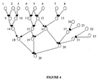
- sub-network N t (v) for each node v of the network N, let v 1 be a node for which all fanins are primary inputs.
- Sub-network N t (v) consists of primary inputs, which have a path to v and v itself
- N t (v) consists of all nodes in C 1 , C 2 , ...,C m and all transitive fanouts of nodes in C 1 ,C 2 , ....,C m which have path to v as shown in Figure 4.
- N t (26) If the sub-network N t (26) is generated by following the steps of conventional mapping algorithms, then N t (26) will contain all nodes till the primary inputs.
- N t (26) ⁇ 1, 2, 3, ... , 24, 25, 26 ⁇
Landscapes
- Engineering & Computer Science (AREA)
- Computer Hardware Design (AREA)
- Physics & Mathematics (AREA)
- Theoretical Computer Science (AREA)
- Evolutionary Computation (AREA)
- Geometry (AREA)
- General Engineering & Computer Science (AREA)
- General Physics & Mathematics (AREA)
- Design And Manufacture Of Integrated Circuits (AREA)
- Logic Circuits (AREA)
Applications Claiming Priority (2)
| Application Number | Priority Date | Filing Date | Title |
|---|---|---|---|
| IN632DE2003 | 2003-04-25 | ||
| INDE06322003 | 2003-04-25 |
Publications (2)
| Publication Number | Publication Date |
|---|---|
| EP1473644A2 true EP1473644A2 (de) | 2004-11-03 |
| EP1473644A3 EP1473644A3 (de) | 2005-09-21 |
Family
ID=32982881
Family Applications (1)
| Application Number | Title | Priority Date | Filing Date |
|---|---|---|---|
| EP04009701A Ceased EP1473644A3 (de) | 2003-04-25 | 2004-04-23 | Verfahren zur Abbildung eines logischen Schaltkreises auf eine programmierbare Nachschlagetabelle |
Country Status (2)
| Country | Link |
|---|---|
| US (1) | US7191427B2 (de) |
| EP (1) | EP1473644A3 (de) |
Families Citing this family (4)
| Publication number | Priority date | Publication date | Assignee | Title |
|---|---|---|---|---|
| US7308671B1 (en) * | 2004-12-06 | 2007-12-11 | Altera Corporation | Method and apparatus for performing mapping onto field programmable gate arrays utilizing fracturable logic cells |
| US7418690B1 (en) | 2005-04-29 | 2008-08-26 | Altera Corporation | Local searching techniques for technology mapping |
| US10275557B1 (en) * | 2010-01-08 | 2019-04-30 | Altera Corporation | Method and apparatus for performing incremental compilation using structural netlist comparison |
| WO2014132670A1 (ja) * | 2013-03-01 | 2014-09-04 | アトナープ株式会社 | 再構成する情報を生成する装置および方法 |
Family Cites Families (5)
| Publication number | Priority date | Publication date | Assignee | Title |
|---|---|---|---|---|
| US6205579B1 (en) * | 1996-10-28 | 2001-03-20 | Altera Corporation | Method for providing remote software technical support |
| US6195788B1 (en) * | 1997-10-17 | 2001-02-27 | Altera Corporation | Mapping heterogeneous logic elements in a programmable logic device |
| US6336208B1 (en) * | 1999-02-04 | 2002-01-01 | Xilinx, Inc. | Delay optimized mapping for programmable gate arrays with multiple sized lookup tables |
| US7124392B2 (en) * | 2002-09-27 | 2006-10-17 | Stmicroelectronics, Pvt. Ltd. | Mapping of programmable logic devices |
| US6871328B1 (en) * | 2002-11-14 | 2005-03-22 | Altera Corporation | Method for mapping logic design memory into physical memory device of a programmable logic device |
-
2004
- 2004-04-23 US US10/830,862 patent/US7191427B2/en not_active Expired - Fee Related
- 2004-04-23 EP EP04009701A patent/EP1473644A3/de not_active Ceased
Non-Patent Citations (1)
| Title |
|---|
| None |
Also Published As
| Publication number | Publication date |
|---|---|
| US20050039157A1 (en) | 2005-02-17 |
| US7191427B2 (en) | 2007-03-13 |
| EP1473644A3 (de) | 2005-09-21 |
Similar Documents
| Publication | Publication Date | Title |
|---|---|---|
| Hauck et al. | An evaluation of bipartitioning techniques | |
| Sangiovanni-Vincentelli et al. | Synthesis method for field programmable gate arrays | |
| US8122396B1 (en) | Local searching techniques for technology mapping | |
| US20020178432A1 (en) | Method and system for synthesizing a circuit representation into a new circuit representation having greater unateness | |
| Cong et al. | Technology mapping for FPGAs with embedded memory blocks | |
| US9026967B1 (en) | Method and apparatus for designing a system on multiple field programmable gate array device types | |
| GB2310064A (en) | Hybrid programmable logic | |
| Cong et al. | Boolean matching for LUT-based logic blocks with applications to architecture evaluation and technology mapping | |
| US8667435B1 (en) | Function symmetry-based optimization for physical synthesis of programmable integrated circuits | |
| Kubica et al. | SMTBDD: New form of BDD for logic synthesis | |
| US8793629B1 (en) | Method and apparatus for implementing carry chains on FPGA devices | |
| US6957412B1 (en) | Techniques for identifying functional blocks in a design that match a template and combining the functional blocks into fewer programmable circuit elements | |
| Lin et al. | Optimal simultaneous mapping and clustering for FPGA delay optimization | |
| Chen et al. | Simultaneous logic decomposition with technology mapping in FPGA designs | |
| Venayagamoorthy et al. | Swarm intelligence for digital circuits implementation on field programmable gate arrays platforms | |
| EP1473644A2 (de) | Verfahren zur Abbildung eines logischen Schlatkreises auf eine programmierbare Nachschlagetabelle | |
| Chtourou et al. | On exploiting partitioning-based placement approach for performances improvement of 3d fpga | |
| Chen et al. | A technology mapping algorithm for CPLD architectures | |
| Naseer et al. | Direct mapping of RTL structures onto LUT-based FPGA's | |
| EP1510950A2 (de) | Verfahren zur Bestimmung des maximalen Volumens und des minimalen Schnittes eines Netzwerkes von verbundenen Knoten | |
| US7020864B1 (en) | Optimized technology mapping techniques for programmable circuits | |
| Cong et al. | A Theory on Partially-Dependent Functional Decomposition with Application in LUT-based FPGA | |
| US7509597B1 (en) | Method and apparatus for performing post-placement functional decomposition on field programmable gate arrays using binary decision diagrams | |
| Farooq et al. | The effect of LUT and cluster size on a tree based FPGA architecture | |
| Ling et al. | FPGA programmable logic block evaluation using quantified Boolean satisfiability |
Legal Events
| Date | Code | Title | Description |
|---|---|---|---|
| PUAI | Public reference made under article 153(3) epc to a published international application that has entered the european phase |
Free format text: ORIGINAL CODE: 0009012 |
|
| AK | Designated contracting states |
Kind code of ref document: A2 Designated state(s): AT BE BG CH CY CZ DE DK EE ES FI FR GB GR HU IE IT LI LU MC NL PL PT RO SE SI SK TR |
|
| AX | Request for extension of the european patent |
Extension state: AL HR LT LV MK |
|
| PUAL | Search report despatched |
Free format text: ORIGINAL CODE: 0009013 |
|
| AK | Designated contracting states |
Kind code of ref document: A3 Designated state(s): AT BE BG CH CY CZ DE DK EE ES FI FR GB GR HU IE IT LI LU MC NL PL PT RO SE SI SK TR |
|
| AX | Request for extension of the european patent |
Extension state: AL HR LT LV MK |
|
| 17P | Request for examination filed |
Effective date: 20060317 |
|
| AKX | Designation fees paid |
Designated state(s): DE FR GB IT |
|
| 17Q | First examination report despatched |
Effective date: 20070608 |
|
| RAP1 | Party data changed (applicant data changed or rights of an application transferred) |
Owner name: STMICROELECTRONICS PVT. LTD. |
|
| RAP1 | Party data changed (applicant data changed or rights of an application transferred) |
Owner name: SICRONIC REMOTE KG, LLC |
|
| STAA | Information on the status of an ep patent application or granted ep patent |
Free format text: STATUS: THE APPLICATION HAS BEEN REFUSED |
|
| 18R | Application refused |
Effective date: 20120628 |