EP1469330A1 - Temperature control element, temperature control component, and waveguide optical module - Google Patents
Temperature control element, temperature control component, and waveguide optical module Download PDFInfo
- Publication number
- EP1469330A1 EP1469330A1 EP03731834A EP03731834A EP1469330A1 EP 1469330 A1 EP1469330 A1 EP 1469330A1 EP 03731834 A EP03731834 A EP 03731834A EP 03731834 A EP03731834 A EP 03731834A EP 1469330 A1 EP1469330 A1 EP 1469330A1
- Authority
- EP
- European Patent Office
- Prior art keywords
- plate
- pedestal
- heater
- contact
- temperature control
- Prior art date
- Legal status (The legal status is an assumption and is not a legal conclusion. Google has not performed a legal analysis and makes no representation as to the accuracy of the status listed.)
- Granted
Links
Images


Classifications
-
- G—PHYSICS
- G02—OPTICS
- G02B—OPTICAL ELEMENTS, SYSTEMS OR APPARATUS
- G02B6/00—Light guides; Structural details of arrangements comprising light guides and other optical elements, e.g. couplings
- G02B6/10—Light guides; Structural details of arrangements comprising light guides and other optical elements, e.g. couplings of the optical waveguide type
- G02B6/12—Light guides; Structural details of arrangements comprising light guides and other optical elements, e.g. couplings of the optical waveguide type of the integrated circuit kind
- G02B6/12007—Light guides; Structural details of arrangements comprising light guides and other optical elements, e.g. couplings of the optical waveguide type of the integrated circuit kind forming wavelength selective elements, e.g. multiplexer, demultiplexer
-
- G—PHYSICS
- G02—OPTICS
- G02B—OPTICAL ELEMENTS, SYSTEMS OR APPARATUS
- G02B6/00—Light guides; Structural details of arrangements comprising light guides and other optical elements, e.g. couplings
- G02B6/24—Coupling light guides
- G02B6/42—Coupling light guides with opto-electronic elements
- G02B6/4201—Packages, e.g. shape, construction, internal or external details
- G02B6/4266—Thermal aspects, temperature control or temperature monitoring
- G02B6/4268—Cooling
- G02B6/4271—Cooling with thermo electric cooling
-
- G—PHYSICS
- G02—OPTICS
- G02B—OPTICAL ELEMENTS, SYSTEMS OR APPARATUS
- G02B6/00—Light guides; Structural details of arrangements comprising light guides and other optical elements, e.g. couplings
- G02B6/10—Light guides; Structural details of arrangements comprising light guides and other optical elements, e.g. couplings of the optical waveguide type
- G02B6/12—Light guides; Structural details of arrangements comprising light guides and other optical elements, e.g. couplings of the optical waveguide type of the integrated circuit kind
- G02B2006/12133—Functions
- G02B2006/12135—Temperature control
-
- G—PHYSICS
- G02—OPTICS
- G02B—OPTICAL ELEMENTS, SYSTEMS OR APPARATUS
- G02B6/00—Light guides; Structural details of arrangements comprising light guides and other optical elements, e.g. couplings
- G02B6/24—Coupling light guides
- G02B6/42—Coupling light guides with opto-electronic elements
- G02B6/4201—Packages, e.g. shape, construction, internal or external details
Definitions
- Such a temperature controller is known from the disclosure in JP-A-2001-116936.
- the disclosed temperature controller is used in a quartz-array waveguide type optical module in which a heater is provided on a plate, which appears as a ceramic substrate, whose thermal expansion coefficient is 5 ppm/°C or less and thermal conductivity is 100 W/m ⁇ K, the plate is held on a pedestal and an optical waveguide is formed on the plate.
- the present invention has a primary object to overcome the above-mentioned drawbacks of the related art by providing a waveguide type optical module having a good wavelength demultiplexing characteristic.
- the present invention has another object to provide a temperature controller and temperature control element for use in the waveguide type optical module showing a highly homogeneous plate-surface temperature distribution.
- the Inventors of the present invention made many experiments and researches and found that when the area of contact between the pedestal and plate was too large (32% or more), the temperature distribution was not homogeneous in some places on the surface of the temperature control element. When the contact area is simply reduced, the plate will be warped or distorted, leading to impossibility of an homogeneous plate-surface temperature distribution, and rather a trouble will take place. On this account, the Inventors decided to increase the contact area to flatten the plate first and adjust the surface roughness of the area of contact between the pedestal and plate or interpose a heat insulator between the pedestal and plate in order to overcome the problem of the inhomogeneous temperature distribution on the plate.
- the flatness (warping) of the plate can be less than 50 ⁇ m, and thus even if the optical waveguide is mounted on the plate, the element will not have the optical axis thereof displaced by inclination or incur large propagation loss of light.
- the surfaces of the plate and heater (heat absorber) and the surface of the pedestal are roughened to prevent any easy heat conduction, or the thermal insulation is laid between the plate and heater and the pedestal to prevent the heat from being dissipated from the contact between the plate and pedestal in order to attain both the flatness (warping) of the plate and homogeneous temperature distribution over the plate surface.
- the plate is supported on the pedestal in contact with the edge thereof. With this manner of supporting, any temperature deviation will not easily take place in the central portion of the plate on which the waveguide is mounted.
- the pedestal is formed like a circular or square frame (cylinder or square column) and thus has a space defined inside thereof, air can be stayed in this space to store the heat, thereby effectively prevent any inhomogeneous temperature distribution from taking place.
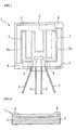
- FIGS. 1 to 8 show an embodiment of each of the temperature control element, temperature controller and waveguide type optical module according to the present invention.
- the temperature control element is generally indicated with a reference 1.
- the temperature control element 1 includes a plate 2 and a heater 3 disposed on a side (non-heating side or rear side) opposite to a heating side of the plate 2 on which a waveguide is disposed.
- a Peltier element as a heat absorber may be provided in place of the heater 3.
- the Peltier element has the functions of both the heater and heat absorber.
- the heater or Peltier element may be provided in the plate element 3.
- pads 4 On which a thermistor chip and platinum resistance chip, used for measurement of a temperature, are mounted, heater power lead wires 7 for electrical connection with the pads 4, and thermistor lead wires 8, and a thermistor chip and platinum resistance chip are mounted on the pads 4 to measure a temperature for the purpose of temperature control.
- the plate 2 may be formed from a metal plate, ceramic plate or resin plate.
- the metal plate include an aluminum plate, copper plate and the like.
- the ceramic plate may include more than one selected from among a nitride ceramics, carbide ceramics, oxide ceramics and carbon.
- a nitride ceramics and carbide ceramics are smaller in thermal expansion coefficient than the metal and considerably greater in mechanical strength than the metal, a thin ceramic plate will not be warped or distorted even when heated. Therefore, the plate 2 can be formed from a thin and lightweight ceramic plate.
- such a ceramic plate is characterized in that the surface temperature thereof will quickly respond to a change in temperature of a resistance heater because of the high heat conductivity and small thickness of the ceramic plate. Therefore, the ceramic plate can advantageously have the surface temperature thereof controlled when changing the temperature of the resistance heater by changing the voltage or current supplied to the heater.
- the aluminum nitride is most preferable for forming the plate 2 because it has a highest heat conductivity as 180 W/m ⁇ K and it is outstanding in temperature response.
- the ceramic used as a material for the plate 2 shows a small thermal expansion coefficient and has only a small difference in thermal expansion from a waveguide 12 even when the temperature becomes high, the waveguide 12 will not be broken and separated from the temperature control element (plate) 1.
- the plate 2 and heater (or heat absorber) 3 have the mean surface roughness Ra (Ra2) (defined in JIS B 0601) thereof adjusted by sand-blasting to more than 0.025 ⁇ m, and have, in relation with the pedestal, the sum including the surface roughness Ra1 of the pedestal adjusted to more than 0.05 ⁇ m.
- Ra mean surface roughness
- the plate 2 is supported on a pedestal 5 shaped like a square frame in contact on the rear-side edge thereof.
- the pedestal 5 is cut square at the top thereof to form a concavity for receiving the plate 2 and heater 3 therein. Namely, the pedestal 5 is thus cut to form a step 5a (in which the plate 2 is fitted at the edge thereof) which defines the concavity.
- the pedestal 2 is thus formed to have a frame-like shape.
- the pedestal 5 is countersunk except for the edge thereof so that the plate 2 is fitted on the step 5a and the upper surface of the plate 2 will be flush with the upper surface of the pedestal 5.
- the pedestal 5 there should preferably be formed a lead-in port for leading out the lead wires 7 for supplying power to the heater 3 or heat absorber and the lead wires 8 for supplying power to the thermistor chip. That is to say, all the edge of the plate 2 may not be in contact with the pedestal 5. It should be noted that the plate 2 should preferably be fixed with fixtures 6 to the pedestal 5.
- FIG 3 is an axial sectional view of the temperature controller.
- the temperature controller according to the present invention has the plate 2 wholly fixed by fitting in the concavity defined by the step 5a in the pedestal 5.
- the temperature controller of the aforementioned structure is supported on the pedestal 5 inside the casing 9.
- the plate 2 should be supported on the pedestal 5 in contact with the edge thereof, which assures an excellent homogeneity of temperature distribution over the surface of the plate 2.
- the plate 2 is fixed by fitting at the end face thereof as well to the step 5a formed in the upper portion of the frame-shaped pedestal 5, the end face of the plate 2 is not exposed to any fluidic atmosphere like air and the heat is stored with an improved efficiency, so that the heat will be distributed more homogeneously over the surface of the plate 2.
- the surface of the pedestal 5 which is in contact with the plate 2, heater 3 and the like has the mean surface roughness Ra (Ra1) (defined in JIS B 0601) thereof adjusted by sand-blasting to more than 0.025 ⁇ m, and have, in relation with the pedestal, the sum including the surface roughness Ra2 of the plate adjusted to more than 0.05 ⁇ m.
- Ra1 defined in JIS B 0601
- the plate 2 may be supported on the pedestal 5 with a thermal insulation 13 being interposed at the contact between the temperature control element 1 and pedestal 5 as shown in FIG 7, instead of adjusting the surface roughness as mentioned above.
- the thermal insulation 13 will provide a heat resistance to limit the heat conduction from the plate 2 to the pedestal 5 and inhibit the heat dissipation from the edge of the plate 2, whereby a homogeneous temperature distribution can be maintained over the surface of the plate 2.
- the thermal insulation 13 used in the present invention may be a rein or inorganic binder.
- the resin at least one or more should desirably be selected from epoxy, phenol, polyimide and silicone resins.
- the inorganic binder at least one or more should desirably be selected from silica sol and alumina sol.
- the resin and binder should preferably contain components which will improve the heat insulation, such as bubbles, fibers or the like.
- the pedestal 5 may be formed from ceramic, metal or resin but the heat conductivity of such a material should desirably be less than 50 W/m ⁇ K which will not lead to any heat conduction-caused occurrence of an inhomogeneous temperature distribution on the plate.
- the ceramics may be an alumina, quartz, cordierite or the like. Also, even when a silicon carbide (SiC) or aluminum nitride (AIN), having a high heat conductivity, is used to form the pedestal 5, the heat conductivity can be lowered by processing this material into a porous one.
- the metal may be a one whose heat conductivity is low, such as a nickel (Ni) alloy.
- the resin may be a glass epoxy or glass polyimide. In this case, the pedestal 5 is formed by punching and countersinking the resin substrate.
- the heater 3 may be formed on the non-heating side (rear side) of the plate 2 or buried in the plate 2.
- the heater 3 should desirably be formed at a depth of less than 60% of the plate thickness from the side of the plate opposite to the heating side (far from the heating side). If it is buried at a depth of more than 60%, namely, if it is positioned too near to the heating side, the heat in the plate 2 will not sufficiently be dissipated, causing an inhomogeneous temperature distribution on the heating side.
- each layer should desirably be such that a resistance heater is formed in any of the layers and each layer appears to include one resistance heater when viewed from the heating side of the plate 2.
- Such a pattern may be a zigzag layout, for example.
- the heater 3 may be buried in the plate 2 and partially exposed to outside the plate 2.
- a conductive paste containing metal particles should be applied to the surface of the plate 2 to form a conductive paste layer having a predetermined pattern, and then the conductive paste pattern be baked to sinter the metal particles on the plate surface.
- the metal sintering may be such that the metal particles, and the metal particles and ceramics, are welded to each other.
- the heater 3 In case the heater 3 is buried in the plate 2, its thickness should preferably be within a range of 1 to 50 ⁇ m. When the heater 3 is to be formed on the surface of the plate 2, its thickness should preferably be within a range of 1 to 30 ⁇ m, and more preferably within a range of 1 to 10 ⁇ m.
- the heater 3 In case the heater 3 is formed buried in the plate 2, its width should preferably be within a range of 5 to 20 ⁇ m. On the other hand, in case the heater 3 is formed on the surface of the plate 2, it should preferably have a width falling within a range of 0.1 to 20 mm, and more preferably within a range of 0.1 to 5 mm.
- the heater 3 can be varied in resistance by changing its width and thickness.
- the aforementioned thickness and width are most practical ones. The smaller the thickness and width, the higher the resistance becomes.
- the heater when it is formed buried in the plate, the heater can be thicker and wider but the surface temperature distribution will be correspondingly inhomogeneous. In this case, it is necessary to design the heater which has an increased width.
- the heater 3 may be formed from a high melting-point metal such as tungsten, molybdenum or the like or a carbide such as a carbide of tungsten, molybdenum or the like, and thus the resistance of the heater 3 can be increased. Therefore, the heater 3 may be formed thick against breakage. Accordingly, the heater 3 should desirably be formed to have the aforementioned thickness and width.
- the heater With the heater being positioned as above, as the heat generated by the heater is propagated, it will be dispersed to the entire plate and the temperature will be distributed homogeneously over the side thereof heating the waveguide.
- the heater may have a sectional form, either rectangular or elliptic but the section should desirably be flat since this form contributes to easier heat dissipation toward the heating side of the plate and a homogeneous temperature distribution on the heating side.
- the material of the resistance heater is not limited to the conductive paste but it should preferably contain resin, solvent, thickener, etc. in addition to metal particles or conductive ceramics which add to an electro-conductivity of the heater.
- the metal particles as a material of the heater 3 should desirably be a noble metal (such as gold, silver, platinum or palladium), lead, tungsten, molybdenum, nickel or the like.
- the material should more preferably be one of the noble metals (gold, silver, platinum and palladium).
- These metals may be used singly or in combination, but more than two of them should desirably be used in combination since they are not easily oxidizable and has a sufficient resistance for heat generation.
- the above-mentioned conductive ceramics include carbides of tungsten and molybdenum. These ceramics may be used singly or more than two of them be used in combination.
- the particle size of the metal or ceramic particles should preferably be within a range of 0.1 to 100 ⁇ m. If the size is less than 0.1 ⁇ m, the particles are easily oxidizable. On the other hand, the particles of more than 100 ⁇ m in size are not easy to sinter and have a higher resistance.
- the metal particles may be either globular or squamate, or may include globular and squamate ones.
- the squamate or globular/squamate metal particles can hold metal oxide between them, and contribute to a positive adherence between the resistance heater and nitride ceramics or the like as well as to an increase resistance of the heater.
- the metal oxide should preferably be at least one selected from a group of lead oxide, zinc oxide, silica, boron oxide (B 2 O 3 ), alumina, yttria and titania, for example. These oxides permits to improve the adherence between the metal particles and nitride or carbide ceramics without increasing the resistance of the resistance heater.
- the amounts of the above-mentioned metal oxides namely, lead oxide, zinc oxide, silica, boron oxide (B 2 O 3 ), alumina, yttria and titania should desirably be adjusted to 1 to 10 % by weight, 1 to 30 % by weight, 5 to 50 % by weight, 20 to 70 % by weight, 1 to 10 % by weight, 1 to 50 % by weight and 1 to 50 % by weight, respectively, with the sum thereof being not over 100% by weight.
- the amounts of these oxides within the above ranges, respectively, it is possible to improve the adherence of the metal particles, especially with the nitride ceramics.
- the heater may be formed from a metal foil or wire.
- the metal foil may be a nickel foil or stainless steel foil. It should desirably be etched to form a pattern of the resistance heater. The metal foils thus patterned may be attached to each other to form the resistance heater.
- the metal wire may be a tungsten or molybdenum wire, for example.
- a metal coating layer should desirably be formed on the surface of the heater in order to prevent the internal sintered metal from being oxidized and having the resistance thereof changed.
- the metal coating layer should preferably be 0.1 to 10 ⁇ m thick.
- the metal used to for the metal coating layer is not limited to any special one but it may be any metal which is non-oxidizable. More specifically, the metal may be gold, silver, palladium, platinum, nickel or the like, for example. These metals may be used singly or two or more of them be used in combination. Among others, nickel should preferably be used to form the metal coating layer.
- the heater has to be connected to the lead wires 7 for connection to the power source.
- the connection is made by soldering or brazing.
- a heat absorber may be used instead of the heater.
- the heat absorber may be a Peltiert element.
- the Peltier element may be connected to the lead wires 7 with an adhesive or any physical means such as screw or spring.
- the waveguide type optical module generally indicated with a reference 100 includes primarily the aforementioned temperature controller element composed of the temperature control element 1 and pedestal 5, Y-branched waveguide 12 and casing 11.
- the waveguide 12 is connected to an input optical fiber 9 and output optical fiber 9', for example, to multi/demultiplex the light wavelength.
- the waveguide 12 should advantageously be a quartz-array waveguide of which the wavelength demultiplexing characteristic varies depending upon the temperature. It should be noted that in FIG. 8, references 10 and 10' indicate fiber fixtures.
- the casing 11 is of a box-shaped structure having a lead-out port through which the aforementioned input and output optical fibers 9 and 9' and lead wires 7 and 8 are led out.
- the temperature control element 1 is supported in air on the pedestal 5 and the waveguide 12 is fixed in contact on the heating side surface of the temperature control element 1.
- the heat homogeneously distributed over the plate surface of the temperature control element 1 can homogeneously be conducted to the waveguide 12 in a short time, whereby the heat dissipation and power consumption can considerably be reduced.
- the wavelength variation in the wavelength demultiplexing characteristic of the waveguide 12 can be limited to positively stabilize the wavelength demultiplexing characteristic.
- the optical waveguide 12 used in the present invention may be either the quartz array type waveguide or a resin-made waveguide formed from polyimide fluoride or the like. It may be a semiconductor laser.
- the optical waveguide 12 may be fixed on the temperature control element 1 mechanically with a screw or spring, not with an adhesive.
- Example 1 and comparative example 1 are comparative example 1 and comparative example 1:
- the pedestal 5 was prepared in which the ratios in area of contact between the pedestal 5 and ceramic plate 2 with the rear-surface area of the ceramic plate 2 (will be referred to simply as "contact area ratio” hereunder) were within a range of 10 to 80 %.
- the flatness (warping) was measured with the ceramic plate 2 supported on each of the pedestals 5 different in contact area ratio from each other.
- the pedestal 5 was in contact with the ceramic plate 2 at the edge and end face of the latter (will be referred to as "edge/end face” hereunder).
- edge/end face In addition to the pedestals which were in contact with the ceramic plate as above, there were prepared a pedestal which was in contact with the plate 2 at an inner portion of the latter (nearer to the center) and a pedestal which was in contact with the plate 2 at the edge of the.
- Several types of such pedestals 5 each having contact area ratios of 10 to 80 % were prepared.
- the flatness (warping) was measured with the ceramic plate 2 supported on each of such additional pedestals 5. The test results are shown in FIG 9.
- the pedestals each having a contact area ratio of less than 30% were taken as acceptable ones while the pedestals each having a contact area ratio of more than 30% were taken as comparative ones.
- FIG 13 shows a photo taken of the temperature distribution on the ceramic plate by the thermo-viewer with the temperature set to 80°C.
- the red frame in the photo indicates an area where the temperature control element is disposed. The temperature difference in this area was observed to be small ( ⁇ T ⁇ 1°C).
- Example 2 and comparative example 2 are comparative example 2 and comparative example 2:
- the example 2 was tested under basically same conditions as in the testing on the example 1 except that the plate was cooled by a Peltier-effect element fixed with an epoxy resin adhesive to the plate (namely, not heated by the heater 3).
- the homogeneity of plate-surface temperature distribution is represented by the difference ⁇ T between highest and lowest temperatures measured with the thermo-viewer set to 5°C.
- the test results are shown in FIG. 11.
- the example 3 was tested under basically same conditions as in the testing on the example 1 except that the raw molding was formed from silicone carbide, not from the aluminum nitride. More specifically, a paste was prepared from a mixture of silicon carbide (by Yakushima Electric, 1.1 ⁇ m in mean particle size) in 100% by weight, B 4 C (1 ⁇ m in mean particle size) in 4% by weight, acrylic resin binder in 11.5% by weight, dispersant in 0.5% by weight and alcohol containing 1-buthanol and ethanol in 53% by weight. It was molded by the doctor blade method to form a plurality of raw moldings of 0.47 mm in thickness. Next, the raw moldings were dried at 80°C for 5 hours, and were punched to form a portion which would be a lead-out port through which connection is to be made external terminals.
- a conductive paste formed from a mixture of tungsten carbide particles of 1.1 ⁇ m in mean particle size in 100% by weight, acrylic resin binder in 3.0% by weight, ⁇ -terpineol solvent in 3.5% by weight and dispersant in 0.3% by weight was filled in the punched portion for the lead-out port in the raw moldings to form a conductive paste layer. Further, a glass paste was applied to the raw molding and then a conductive paste was printed over the glass paste to form a wiring pattern and a pad on which a heater 3 and thermistor were to be mounted.
- the raw moldings were stacked one on another.
- the stack was sintered in a nitrogen atmosphere at 1980°C under a pressure of 200 kg/cm 2 to form a ceramic plate 2.
- the ceramic plate 2 was cut for the mounting pad to be exposed to outside, and a thermistor was mounted by soldering on the pad to form a temperature control element (heater plate) 1 of 1.5 mm in thickness.
- FIG 9 A flatness (warping) similar to that in the example 1 is shown in FIG 9, and the homogeneity of plate-surface temperature distribution is shown in FIG 12.
- the example 4 was tested under similar conditions to those in the testing on the example 1 except that the plate was applied with silicone resin, not roughened by sand-blasting, and fitted in the pedestal 5. The test was started after the silicone resin became dry.
- the silicone resin layer 13 was 100 ⁇ m thick, which yielded a flatness (warp) of 10 ⁇ m. With the thermo-viewer set to 80°C, the difference ⁇ T was observed to be 0.1°C.
- the comparative example 4 was tested under basically same conditions as those in the testing on the example 1 except that the step 5a was formed to coincide with the patterns of the heater 3 and pad 4 when forming the step 5a by counter-sinking the pedestal 5.
- the area of contact between the heater plate and pedestal 5 was 100%.
- the flatness (warping) was 10 ⁇ m.
- the thermo-viewer set to 80°C the difference ⁇ T was observed to be 2°C.
- the temperature control element, and the temperature controller and waveguide type optical module, each using the temperature control element are superior in homogeneity of the plate-surface temperature distribution of the temperature control element, have a superb optical waveguide characteristic supporting the multi-channeling, that is, having a stable wavelength demultiplexing characteristic.
Landscapes
- Physics & Mathematics (AREA)
- General Physics & Mathematics (AREA)
- Optics & Photonics (AREA)
- Engineering & Computer Science (AREA)
- Microelectronics & Electronic Packaging (AREA)
- Optical Integrated Circuits (AREA)
Abstract
Description
Claims (14)
- A temperature control element including a plate having a heater or heat absorber provided on the non-heating side thereof or buried therein, wherein:the total area of contact between a pedestal provided to support the plate thereon in contact with mainly the non-heating side and the plate including the heater or heat absorber is over 30% of the area of the non-heating side of the plate; andthe sum of surface roughness Ra2 of the plate and heater or heat absorber at a portion where it is in contact with the pedestal and that at the side of the plate at the pedestal side is over 0.05 µm.
- The element according to claim 1, wherein the pedestal supports the plate in contact with the edge and/or end face at the non-heating side of the non-heating side of the plate.
- The element according to claim 1 or 2, wherein the plate is formed from ceramics.
- A temperature controller including a temperature control element and a pedestal to support the temperature control element thereon inside a casing, wherein:the temperature control element includes a plate having a heater or heat absorber provided on the non-heating side thereof or buried therein;the total area of contact between a pedestal provided to support the plate thereon in contact with mainly the non-heating side and the plate including the heater or heat absorber is over 30% of the area of the non-heating side of the plate; andthe sum of surface roughness Ra1 of the pedestal at a portion where it is in contact with the plate and heater or heat absorber and surface roughness Ra2 of the plate and heater or heat absorber at a portion where it is in contact with the pedestal and is over 0.05 µm.
- The controller according to claim 4, wherein the pedestal supports the plate in contact with the edge and/or end face at the non-heating side of the non-heating side of the plate.
- The controller according to claim 4 or 5, wherein the plate is formed from ceramics.
- A waveguide type optical module in which a temperature control element is supported in air on a pedestal inside a casing and an optical waveguide is mounted on the temperature control element, wherein:the temperature control element includes a plate having a heater or heat absorber provided on the non-heating side thereof or buried therein;the total area of contact between a pedestal provided to support the plate thereon in contact with mainly the non-heating side and the plate including the heater or heat absorber is over 30% of the area of the non-heating side of the plate; andthe sum of surface roughness Ra1 of the pedestal at a portion where it is in contact with the plate and heater or heat absorber and surface roughness Ra2 of the plate and heater or heat absorber at a portion where it is in contact with the pedestal and that at the side of the plate at the pedestal side is over 0.05 µm.
- A temperature control element including a plate having a heater or heat absorber provided on the non-heating side thereof or buried therein, wherein:a pedestal provided to support the plate thereon in contact with mainly the non-heating side and plate are superposed one on the other with a thermal insulation laid between them; andthe sum of area of contact between the pedestal, and the plate including the heater or heat absorber and superposed on the pedestal with the thermal insulation laid between them, is over 30% of the area of the non-heating side of the plate.
- The element according to claim 8, wherein the pedestal supports the plate in contact with the edge and/or end face at the non-heating side of the latter.
- The element according to claim 8 or 9, wherein the plate is formed from ceramics.
- A temperature controller including a temperature control element and a pedestal provided to support the plate thereon inside a casing, wherein:the temperature control element includes a plate having a heater or heat absorber provided on the non-heating side thereof or buried therein;the pedestal mainly in contact with the non-heating side of the plate and plate are superposed one on the other with a thermal insulation laid between them; andthe sum of area of contact between the pedestal, and the plate including the heater or heat absorber and superposed on the pedestal with the thermal insulation laid between them, is over 30% of the area of the non-heating side of the plate.
- The controller according to claim 11, wherein the pedestal supports the plate in contact with the edge and/or end face at the non-heating side of the latter.
- The controller according to claim 11 or 12, wherein the plate is formed from ceramics.
- A waveguide type optical module in which a temperature control element is supported in on a pedestal inside a casing and an optical waveguide is mounted on the temperature control element, wherein:the temperature control element includes a plate having a heater or heat absorber provided on the non-heating side thereof or buried therein;the pedestal mainly in contact with the non-heating side of the plate and plate are superposed one on the other with a thermal insulation laid between them; andthe sum of area of contact between the pedestal, and the plate including the heater or heat absorber and superposed on the pedestal with the thermal insulation laid between them, is over 30% of the area of the non-heating side of the plate.
Applications Claiming Priority (3)
| Application Number | Priority Date | Filing Date | Title |
|---|---|---|---|
| JP2002015930 | 2002-01-24 | ||
| JP2002015930 | 2002-01-24 | ||
| PCT/JP2003/000636 WO2003062878A1 (en) | 2002-01-24 | 2003-01-24 | Temperature control element, temperature control component, and waveguide optical module |
Publications (3)
| Publication Number | Publication Date |
|---|---|
| EP1469330A1 true EP1469330A1 (en) | 2004-10-20 |
| EP1469330A4 EP1469330A4 (en) | 2009-09-23 |
| EP1469330B1 EP1469330B1 (en) | 2013-09-25 |
Family
ID=27606123
Family Applications (1)
| Application Number | Title | Priority Date | Filing Date |
|---|---|---|---|
| EP03731834.2A Expired - Lifetime EP1469330B1 (en) | 2002-01-24 | 2003-01-24 | Temperature control element, temperature control component, and waveguide optical module |
Country Status (4)
| Country | Link |
|---|---|
| US (1) | US20050141845A1 (en) |
| EP (1) | EP1469330B1 (en) |
| TW (1) | TW200302363A (en) |
| WO (1) | WO2003062878A1 (en) |
Families Citing this family (3)
| Publication number | Priority date | Publication date | Assignee | Title |
|---|---|---|---|---|
| US7132628B2 (en) * | 2004-03-10 | 2006-11-07 | Watlow Electric Manufacturing Company | Variable watt density layered heater |
| JP2012256026A (en) * | 2011-05-13 | 2012-12-27 | Japan Oclaro Inc | Optical phase adjusting element and demodulator using the same |
| JP2020181024A (en) * | 2019-04-23 | 2020-11-05 | 富士通株式会社 | Optical transmission module |
Family Cites Families (9)
| Publication number | Priority date | Publication date | Assignee | Title |
|---|---|---|---|---|
| US5147821A (en) * | 1990-09-28 | 1992-09-15 | Motorola, Inc. | Method for making a thermally enhanced semiconductor device by holding a leadframe against a heatsink through vacuum suction in a molding operation |
| US5822848A (en) * | 1996-06-04 | 1998-10-20 | Industrial Technology Research Institute | Lead frame having a detachable and interchangeable die-attach paddle |
| JPH10333190A (en) * | 1997-05-28 | 1998-12-18 | Nec Corp | Light switch |
| US5917272A (en) * | 1998-06-11 | 1999-06-29 | Vectron, Inc. | Oven-heated crystal resonator and oscillator assembly |
| JP2000075152A (en) * | 1998-08-31 | 2000-03-14 | Furukawa Electric Co Ltd:The | Optical module |
| JP2000206348A (en) * | 1999-01-13 | 2000-07-28 | Furukawa Electric Co Ltd:The | Compensation method of light transmission wavelength of optical waveguide circuit |
| JP2001033643A (en) * | 1999-07-21 | 2001-02-09 | Hitachi Cable Ltd | Waveguide type optical module |
| JP2001083340A (en) * | 1999-09-09 | 2001-03-30 | Hitachi Cable Ltd | Optical module package structure |
| JP3665555B2 (en) * | 2000-11-10 | 2005-06-29 | 古河電気工業株式会社 | Optical module |
-
2003
- 2003-01-23 TW TW092101455A patent/TW200302363A/en unknown
- 2003-01-24 US US10/500,866 patent/US20050141845A1/en not_active Abandoned
- 2003-01-24 WO PCT/JP2003/000636 patent/WO2003062878A1/en not_active Ceased
- 2003-01-24 EP EP03731834.2A patent/EP1469330B1/en not_active Expired - Lifetime
Also Published As
| Publication number | Publication date |
|---|---|
| WO2003062878A1 (en) | 2003-07-31 |
| EP1469330B1 (en) | 2013-09-25 |
| EP1469330A4 (en) | 2009-09-23 |
| TW200302363A (en) | 2003-08-01 |
| US20050141845A1 (en) | 2005-06-30 |
Similar Documents
| Publication | Publication Date | Title |
|---|---|---|
| US20040155025A1 (en) | Ceramic heater | |
| US20040060920A1 (en) | Ceramic heater | |
| US20040117977A1 (en) | Ceramic substrate for semiconductor manufacturing and inspecting devices, and method of manufacturing the ceramic substrate | |
| KR100615443B1 (en) | Ceramic heater | |
| JP2002025758A (en) | Hot plate unit | |
| US20030102299A1 (en) | Ceramic heater | |
| JP2002184558A (en) | heater | |
| US20030098299A1 (en) | Ceramic heater | |
| JP2002064133A (en) | Support container and semiconductor manufacturing / inspection equipment | |
| US20040026403A1 (en) | Ceramic heater for semiconductor manufacturing and inspecting devices | |
| EP1469330B1 (en) | Temperature control element, temperature control component, and waveguide optical module | |
| JP2003059789A (en) | Connection structure and semiconductor manufacturing and inspecting apparatus | |
| JP2004296532A (en) | Hot plate unit | |
| EP1475651A1 (en) | Waveguide type optical module, and temperature control component, and temperature control element thereof | |
| JP2002083848A (en) | Semiconductor manufacturing and inspection equipment | |
| JP2001237301A (en) | Ceramic substrate for semiconductor manufacturing and inspection equipment | |
| JP2003287632A (en) | Temperature control element, temperature control component, and waveguide type optical module | |
| JP2001332560A (en) | Semiconductor manufacturing and inspecting device | |
| JP2001085144A (en) | Ceramic heater | |
| JP2002334820A (en) | Ceramic heater for heating semiconductor wafer or liquid crystal substrate | |
| JP2001319758A (en) | Hot plate unit | |
| JP2002319525A (en) | Ceramic heater for semiconductor manufacturing and inspection equipment | |
| JP2001237304A (en) | Ceramic substrate for semiconductor manufacturing/ inspecting device | |
| JP2002260829A (en) | Hot plate unit | |
| WO2024204547A1 (en) | Ceramic structure |
Legal Events
| Date | Code | Title | Description |
|---|---|---|---|
| PUAI | Public reference made under article 153(3) epc to a published international application that has entered the european phase |
Free format text: ORIGINAL CODE: 0009012 |
|
| 17P | Request for examination filed |
Effective date: 20040728 |
|
| AK | Designated contracting states |
Kind code of ref document: A1 Designated state(s): AT BE BG CH CY CZ DE DK EE ES FI FR GB GR HU IE IT LI LU MC NL PT SE SI SK TR |
|
| A4 | Supplementary search report drawn up and despatched |
Effective date: 20090826 |
|
| 17Q | First examination report despatched |
Effective date: 20100628 |
|
| GRAP | Despatch of communication of intention to grant a patent |
Free format text: ORIGINAL CODE: EPIDOSNIGR1 |
|
| INTG | Intention to grant announced |
Effective date: 20130415 |
|
| GRAS | Grant fee paid |
Free format text: ORIGINAL CODE: EPIDOSNIGR3 |
|
| GRAA | (expected) grant |
Free format text: ORIGINAL CODE: 0009210 |
|
| AK | Designated contracting states |
Kind code of ref document: B1 Designated state(s): AT BE BG CH CY CZ DE DK EE ES FI FR GB GR HU IE IT LI LU MC NL PT SE SI SK TR |
|
| REG | Reference to a national code |
Ref country code: GB Ref legal event code: FG4D |
|
| REG | Reference to a national code |
Ref country code: CH Ref legal event code: EP |
|
| REG | Reference to a national code |
Ref country code: AT Ref legal event code: REF Ref document number: 633927 Country of ref document: AT Kind code of ref document: T Effective date: 20131015 |
|
| REG | Reference to a national code |
Ref country code: IE Ref legal event code: FG4D |
|
| REG | Reference to a national code |
Ref country code: DE Ref legal event code: R096 Ref document number: 60344979 Country of ref document: DE Effective date: 20131128 |
|
| PG25 | Lapsed in a contracting state [announced via postgrant information from national office to epo] |
Ref country code: SE Free format text: LAPSE BECAUSE OF FAILURE TO SUBMIT A TRANSLATION OF THE DESCRIPTION OR TO PAY THE FEE WITHIN THE PRESCRIBED TIME-LIMIT Effective date: 20130925 |
|
| REG | Reference to a national code |
Ref country code: AT Ref legal event code: MK05 Ref document number: 633927 Country of ref document: AT Kind code of ref document: T Effective date: 20130925 |
|
| REG | Reference to a national code |
Ref country code: NL Ref legal event code: VDEP Effective date: 20130925 |
|
| PG25 | Lapsed in a contracting state [announced via postgrant information from national office to epo] |
Ref country code: FI Free format text: LAPSE BECAUSE OF FAILURE TO SUBMIT A TRANSLATION OF THE DESCRIPTION OR TO PAY THE FEE WITHIN THE PRESCRIBED TIME-LIMIT Effective date: 20130925 Ref country code: GR Free format text: LAPSE BECAUSE OF FAILURE TO SUBMIT A TRANSLATION OF THE DESCRIPTION OR TO PAY THE FEE WITHIN THE PRESCRIBED TIME-LIMIT Effective date: 20131226 Ref country code: SI Free format text: LAPSE BECAUSE OF FAILURE TO SUBMIT A TRANSLATION OF THE DESCRIPTION OR TO PAY THE FEE WITHIN THE PRESCRIBED TIME-LIMIT Effective date: 20130925 |
|
| PG25 | Lapsed in a contracting state [announced via postgrant information from national office to epo] |
Ref country code: BE Free format text: LAPSE BECAUSE OF FAILURE TO SUBMIT A TRANSLATION OF THE DESCRIPTION OR TO PAY THE FEE WITHIN THE PRESCRIBED TIME-LIMIT Effective date: 20130925 |
|
| PG25 | Lapsed in a contracting state [announced via postgrant information from national office to epo] |
Ref country code: CZ Free format text: LAPSE BECAUSE OF FAILURE TO SUBMIT A TRANSLATION OF THE DESCRIPTION OR TO PAY THE FEE WITHIN THE PRESCRIBED TIME-LIMIT Effective date: 20130925 Ref country code: EE Free format text: LAPSE BECAUSE OF FAILURE TO SUBMIT A TRANSLATION OF THE DESCRIPTION OR TO PAY THE FEE WITHIN THE PRESCRIBED TIME-LIMIT Effective date: 20130925 Ref country code: SK Free format text: LAPSE BECAUSE OF FAILURE TO SUBMIT A TRANSLATION OF THE DESCRIPTION OR TO PAY THE FEE WITHIN THE PRESCRIBED TIME-LIMIT Effective date: 20130925 Ref country code: NL Free format text: LAPSE BECAUSE OF FAILURE TO SUBMIT A TRANSLATION OF THE DESCRIPTION OR TO PAY THE FEE WITHIN THE PRESCRIBED TIME-LIMIT Effective date: 20130925 |
|
| PG25 | Lapsed in a contracting state [announced via postgrant information from national office to epo] |
Ref country code: ES Free format text: LAPSE BECAUSE OF FAILURE TO SUBMIT A TRANSLATION OF THE DESCRIPTION OR TO PAY THE FEE WITHIN THE PRESCRIBED TIME-LIMIT Effective date: 20130925 Ref country code: AT Free format text: LAPSE BECAUSE OF FAILURE TO SUBMIT A TRANSLATION OF THE DESCRIPTION OR TO PAY THE FEE WITHIN THE PRESCRIBED TIME-LIMIT Effective date: 20130925 Ref country code: CY Free format text: LAPSE BECAUSE OF FAILURE TO SUBMIT A TRANSLATION OF THE DESCRIPTION OR TO PAY THE FEE WITHIN THE PRESCRIBED TIME-LIMIT Effective date: 20130925 |
|
| REG | Reference to a national code |
Ref country code: DE Ref legal event code: R097 Ref document number: 60344979 Country of ref document: DE |
|
| PG25 | Lapsed in a contracting state [announced via postgrant information from national office to epo] |
Ref country code: PT Free format text: LAPSE BECAUSE OF FAILURE TO SUBMIT A TRANSLATION OF THE DESCRIPTION OR TO PAY THE FEE WITHIN THE PRESCRIBED TIME-LIMIT Effective date: 20140127 |
|
| PLBE | No opposition filed within time limit |
Free format text: ORIGINAL CODE: 0009261 |
|
| REG | Reference to a national code |
Ref country code: DE Ref legal event code: R119 Ref document number: 60344979 Country of ref document: DE |
|
| STAA | Information on the status of an ep patent application or granted ep patent |
Free format text: STATUS: NO OPPOSITION FILED WITHIN TIME LIMIT |
|
| PG25 | Lapsed in a contracting state [announced via postgrant information from national office to epo] |
Ref country code: LU Free format text: LAPSE BECAUSE OF FAILURE TO SUBMIT A TRANSLATION OF THE DESCRIPTION OR TO PAY THE FEE WITHIN THE PRESCRIBED TIME-LIMIT Effective date: 20140124 Ref country code: IT Free format text: LAPSE BECAUSE OF FAILURE TO SUBMIT A TRANSLATION OF THE DESCRIPTION OR TO PAY THE FEE WITHIN THE PRESCRIBED TIME-LIMIT Effective date: 20130925 Ref country code: MC Free format text: LAPSE BECAUSE OF FAILURE TO SUBMIT A TRANSLATION OF THE DESCRIPTION OR TO PAY THE FEE WITHIN THE PRESCRIBED TIME-LIMIT Effective date: 20130925 |
|
| REG | Reference to a national code |
Ref country code: CH Ref legal event code: PL |
|
| 26N | No opposition filed |
Effective date: 20140626 |
|
| GBPC | Gb: european patent ceased through non-payment of renewal fee |
Effective date: 20140124 |
|
| PG25 | Lapsed in a contracting state [announced via postgrant information from national office to epo] |
Ref country code: DK Free format text: LAPSE BECAUSE OF FAILURE TO SUBMIT A TRANSLATION OF THE DESCRIPTION OR TO PAY THE FEE WITHIN THE PRESCRIBED TIME-LIMIT Effective date: 20130925 |
|
| REG | Reference to a national code |
Ref country code: DE Ref legal event code: R097 Ref document number: 60344979 Country of ref document: DE Effective date: 20140626 |
|
| REG | Reference to a national code |
Ref country code: DE Ref legal event code: R119 Ref document number: 60344979 Country of ref document: DE Effective date: 20140801 |
|
| PG25 | Lapsed in a contracting state [announced via postgrant information from national office to epo] |
Ref country code: CH Free format text: LAPSE BECAUSE OF NON-PAYMENT OF DUE FEES Effective date: 20140131 Ref country code: LI Free format text: LAPSE BECAUSE OF NON-PAYMENT OF DUE FEES Effective date: 20140131 Ref country code: DE Free format text: LAPSE BECAUSE OF NON-PAYMENT OF DUE FEES Effective date: 20140801 |
|
| REG | Reference to a national code |
Ref country code: FR Ref legal event code: ST Effective date: 20140930 |
|
| REG | Reference to a national code |
Ref country code: IE Ref legal event code: MM4A |
|
| PG25 | Lapsed in a contracting state [announced via postgrant information from national office to epo] |
Ref country code: FR Free format text: LAPSE BECAUSE OF NON-PAYMENT OF DUE FEES Effective date: 20140131 Ref country code: GB Free format text: LAPSE BECAUSE OF NON-PAYMENT OF DUE FEES Effective date: 20140124 |
|
| PG25 | Lapsed in a contracting state [announced via postgrant information from national office to epo] |
Ref country code: IE Free format text: LAPSE BECAUSE OF NON-PAYMENT OF DUE FEES Effective date: 20140124 |
|
| PG25 | Lapsed in a contracting state [announced via postgrant information from national office to epo] |
Ref country code: BG Free format text: LAPSE BECAUSE OF FAILURE TO SUBMIT A TRANSLATION OF THE DESCRIPTION OR TO PAY THE FEE WITHIN THE PRESCRIBED TIME-LIMIT Effective date: 20130925 |
|
| PG25 | Lapsed in a contracting state [announced via postgrant information from national office to epo] |
Ref country code: HU Free format text: LAPSE BECAUSE OF FAILURE TO SUBMIT A TRANSLATION OF THE DESCRIPTION OR TO PAY THE FEE WITHIN THE PRESCRIBED TIME-LIMIT; INVALID AB INITIO Effective date: 20030124 Ref country code: TR Free format text: LAPSE BECAUSE OF FAILURE TO SUBMIT A TRANSLATION OF THE DESCRIPTION OR TO PAY THE FEE WITHIN THE PRESCRIBED TIME-LIMIT Effective date: 20130925 |