EP1467604A2 - Techniques for reducing the number of layers in a multilayer signal routing device. - Google Patents
Techniques for reducing the number of layers in a multilayer signal routing device. Download PDFInfo
- Publication number
- EP1467604A2 EP1467604A2 EP04252038A EP04252038A EP1467604A2 EP 1467604 A2 EP1467604 A2 EP 1467604A2 EP 04252038 A EP04252038 A EP 04252038A EP 04252038 A EP04252038 A EP 04252038A EP 1467604 A2 EP1467604 A2 EP 1467604A2
- Authority
- EP
- European Patent Office
- Prior art keywords
- electrically conductive
- channel
- signal
- array
- electrical signals
- Prior art date
- Legal status (The legal status is an assumption and is not a legal conclusion. Google has not performed a legal analysis and makes no representation as to the accuracy of the status listed.)
- Withdrawn
Links
- 238000000034 method Methods 0.000 title claims abstract description 76
- 229910003460 diamond Inorganic materials 0.000 claims description 7
- 239000010432 diamond Substances 0.000 claims description 7
- 230000002411 adverse Effects 0.000 description 5
- 230000003071 parasitic effect Effects 0.000 description 4
- 230000009286 beneficial effect Effects 0.000 description 3
- 238000012986 modification Methods 0.000 description 3
- 230000004048 modification Effects 0.000 description 3
- 230000001902 propagating effect Effects 0.000 description 3
- 230000015572 biosynthetic process Effects 0.000 description 2
- 230000000903 blocking effect Effects 0.000 description 2
- 238000004364 calculation method Methods 0.000 description 2
- 230000000694 effects Effects 0.000 description 2
- 238000003491 array Methods 0.000 description 1
- 230000001174 ascending effect Effects 0.000 description 1
- 230000013011 mating Effects 0.000 description 1
- XLYOFNOQVPJJNP-UHFFFAOYSA-N water Substances O XLYOFNOQVPJJNP-UHFFFAOYSA-N 0.000 description 1
Images





Classifications
-
- H—ELECTRICITY
- H05—ELECTRIC TECHNIQUES NOT OTHERWISE PROVIDED FOR
- H05K—PRINTED CIRCUITS; CASINGS OR CONSTRUCTIONAL DETAILS OF ELECTRIC APPARATUS; MANUFACTURE OF ASSEMBLAGES OF ELECTRICAL COMPONENTS
- H05K1/00—Printed circuits
- H05K1/02—Details
- H05K1/11—Printed elements for providing electric connections to or between printed circuits
- H05K1/115—Via connections; Lands around holes or via connections
-
- F—MECHANICAL ENGINEERING; LIGHTING; HEATING; WEAPONS; BLASTING
- F16—ENGINEERING ELEMENTS AND UNITS; GENERAL MEASURES FOR PRODUCING AND MAINTAINING EFFECTIVE FUNCTIONING OF MACHINES OR INSTALLATIONS; THERMAL INSULATION IN GENERAL
- F16L—PIPES; JOINTS OR FITTINGS FOR PIPES; SUPPORTS FOR PIPES, CABLES OR PROTECTIVE TUBING; MEANS FOR THERMAL INSULATION IN GENERAL
- F16L41/00—Branching pipes; Joining pipes to walls
- F16L41/08—Joining pipes to walls or pipes, the joined pipe axis being perpendicular to the plane of a wall or to the axis of another pipe
- F16L41/12—Joining pipes to walls or pipes, the joined pipe axis being perpendicular to the plane of a wall or to the axis of another pipe using attaching means embracing the pipe
-
- H—ELECTRICITY
- H05—ELECTRIC TECHNIQUES NOT OTHERWISE PROVIDED FOR
- H05K—PRINTED CIRCUITS; CASINGS OR CONSTRUCTIONAL DETAILS OF ELECTRIC APPARATUS; MANUFACTURE OF ASSEMBLAGES OF ELECTRICAL COMPONENTS
- H05K1/00—Printed circuits
- H05K1/02—Details
- H05K1/11—Printed elements for providing electric connections to or between printed circuits
- H05K1/111—Pads for surface mounting, e.g. lay-out
- H05K1/112—Pads for surface mounting, e.g. lay-out directly combined with via connections
-
- H—ELECTRICITY
- H05—ELECTRIC TECHNIQUES NOT OTHERWISE PROVIDED FOR
- H05K—PRINTED CIRCUITS; CASINGS OR CONSTRUCTIONAL DETAILS OF ELECTRIC APPARATUS; MANUFACTURE OF ASSEMBLAGES OF ELECTRICAL COMPONENTS
- H05K1/00—Printed circuits
- H05K1/02—Details
- H05K1/0296—Conductive pattern lay-out details not covered by sub groups H05K1/02 - H05K1/0295
- H05K1/0298—Multilayer circuits
-
- H—ELECTRICITY
- H05—ELECTRIC TECHNIQUES NOT OTHERWISE PROVIDED FOR
- H05K—PRINTED CIRCUITS; CASINGS OR CONSTRUCTIONAL DETAILS OF ELECTRIC APPARATUS; MANUFACTURE OF ASSEMBLAGES OF ELECTRICAL COMPONENTS
- H05K2201/00—Indexing scheme relating to printed circuits covered by H05K1/00
- H05K2201/09—Shape and layout
- H05K2201/09209—Shape and layout details of conductors
- H05K2201/09218—Conductive traces
- H05K2201/09227—Layout details of a plurality of traces, e.g. escape layout for Ball Grid Array [BGA] mounting
-
- H—ELECTRICITY
- H05—ELECTRIC TECHNIQUES NOT OTHERWISE PROVIDED FOR
- H05K—PRINTED CIRCUITS; CASINGS OR CONSTRUCTIONAL DETAILS OF ELECTRIC APPARATUS; MANUFACTURE OF ASSEMBLAGES OF ELECTRICAL COMPONENTS
- H05K2201/00—Indexing scheme relating to printed circuits covered by H05K1/00
- H05K2201/09—Shape and layout
- H05K2201/09209—Shape and layout details of conductors
- H05K2201/09218—Conductive traces
- H05K2201/09236—Parallel layout
-
- H—ELECTRICITY
- H05—ELECTRIC TECHNIQUES NOT OTHERWISE PROVIDED FOR
- H05K—PRINTED CIRCUITS; CASINGS OR CONSTRUCTIONAL DETAILS OF ELECTRIC APPARATUS; MANUFACTURE OF ASSEMBLAGES OF ELECTRICAL COMPONENTS
- H05K2201/00—Indexing scheme relating to printed circuits covered by H05K1/00
- H05K2201/09—Shape and layout
- H05K2201/09209—Shape and layout details of conductors
- H05K2201/09218—Conductive traces
- H05K2201/09263—Meander
-
- H—ELECTRICITY
- H05—ELECTRIC TECHNIQUES NOT OTHERWISE PROVIDED FOR
- H05K—PRINTED CIRCUITS; CASINGS OR CONSTRUCTIONAL DETAILS OF ELECTRIC APPARATUS; MANUFACTURE OF ASSEMBLAGES OF ELECTRICAL COMPONENTS
- H05K2201/00—Indexing scheme relating to printed circuits covered by H05K1/00
- H05K2201/09—Shape and layout
- H05K2201/09209—Shape and layout details of conductors
- H05K2201/095—Conductive through-holes or vias
- H05K2201/09509—Blind vias, i.e. vias having one side closed
-
- H—ELECTRICITY
- H05—ELECTRIC TECHNIQUES NOT OTHERWISE PROVIDED FOR
- H05K—PRINTED CIRCUITS; CASINGS OR CONSTRUCTIONAL DETAILS OF ELECTRIC APPARATUS; MANUFACTURE OF ASSEMBLAGES OF ELECTRICAL COMPONENTS
- H05K2201/00—Indexing scheme relating to printed circuits covered by H05K1/00
- H05K2201/09—Shape and layout
- H05K2201/09209—Shape and layout details of conductors
- H05K2201/095—Conductive through-holes or vias
- H05K2201/09536—Buried plated through-holes, i.e. plated through-holes formed in a core before lamination
-
- H—ELECTRICITY
- H05—ELECTRIC TECHNIQUES NOT OTHERWISE PROVIDED FOR
- H05K—PRINTED CIRCUITS; CASINGS OR CONSTRUCTIONAL DETAILS OF ELECTRIC APPARATUS; MANUFACTURE OF ASSEMBLAGES OF ELECTRICAL COMPONENTS
- H05K2201/00—Indexing scheme relating to printed circuits covered by H05K1/00
- H05K2201/09—Shape and layout
- H05K2201/09209—Shape and layout details of conductors
- H05K2201/095—Conductive through-holes or vias
- H05K2201/09627—Special connections between adjacent vias, not for grounding vias
-
- H—ELECTRICITY
- H05—ELECTRIC TECHNIQUES NOT OTHERWISE PROVIDED FOR
- H05K—PRINTED CIRCUITS; CASINGS OR CONSTRUCTIONAL DETAILS OF ELECTRIC APPARATUS; MANUFACTURE OF ASSEMBLAGES OF ELECTRICAL COMPONENTS
- H05K2201/00—Indexing scheme relating to printed circuits covered by H05K1/00
- H05K2201/10—Details of components or other objects attached to or integrated in a printed circuit board
- H05K2201/10613—Details of electrical connections of non-printed components, e.g. special leads
- H05K2201/10621—Components characterised by their electrical contacts
- H05K2201/10734—Ball grid array [BGA]; Bump grid array
-
- H—ELECTRICITY
- H05—ELECTRIC TECHNIQUES NOT OTHERWISE PROVIDED FOR
- H05K—PRINTED CIRCUITS; CASINGS OR CONSTRUCTIONAL DETAILS OF ELECTRIC APPARATUS; MANUFACTURE OF ASSEMBLAGES OF ELECTRICAL COMPONENTS
- H05K3/00—Apparatus or processes for manufacturing printed circuits
- H05K3/0005—Apparatus or processes for manufacturing printed circuits for designing circuits by computer
-
- H—ELECTRICITY
- H05—ELECTRIC TECHNIQUES NOT OTHERWISE PROVIDED FOR
- H05K—PRINTED CIRCUITS; CASINGS OR CONSTRUCTIONAL DETAILS OF ELECTRIC APPARATUS; MANUFACTURE OF ASSEMBLAGES OF ELECTRICAL COMPONENTS
- H05K3/00—Apparatus or processes for manufacturing printed circuits
- H05K3/40—Forming printed elements for providing electric connections to or between printed circuits
- H05K3/42—Plated through-holes or plated via connections
- H05K3/429—Plated through-holes specially for multilayer circuits, e.g. having connections to inner circuit layers
-
- H—ELECTRICITY
- H05—ELECTRIC TECHNIQUES NOT OTHERWISE PROVIDED FOR
- H05K—PRINTED CIRCUITS; CASINGS OR CONSTRUCTIONAL DETAILS OF ELECTRIC APPARATUS; MANUFACTURE OF ASSEMBLAGES OF ELECTRICAL COMPONENTS
- H05K3/00—Apparatus or processes for manufacturing printed circuits
- H05K3/46—Manufacturing multilayer circuits
- H05K3/4602—Manufacturing multilayer circuits characterized by a special circuit board as base or central core whereon additional circuit layers are built or additional circuit boards are laminated
-
- Y—GENERAL TAGGING OF NEW TECHNOLOGICAL DEVELOPMENTS; GENERAL TAGGING OF CROSS-SECTIONAL TECHNOLOGIES SPANNING OVER SEVERAL SECTIONS OF THE IPC; TECHNICAL SUBJECTS COVERED BY FORMER USPC CROSS-REFERENCE ART COLLECTIONS [XRACs] AND DIGESTS
- Y10—TECHNICAL SUBJECTS COVERED BY FORMER USPC
- Y10T—TECHNICAL SUBJECTS COVERED BY FORMER US CLASSIFICATION
- Y10T29/00—Metal working
- Y10T29/49—Method of mechanical manufacture
- Y10T29/49002—Electrical device making
- Y10T29/49016—Antenna or wave energy "plumbing" making
-
- Y—GENERAL TAGGING OF NEW TECHNOLOGICAL DEVELOPMENTS; GENERAL TAGGING OF CROSS-SECTIONAL TECHNOLOGIES SPANNING OVER SEVERAL SECTIONS OF THE IPC; TECHNICAL SUBJECTS COVERED BY FORMER USPC CROSS-REFERENCE ART COLLECTIONS [XRACs] AND DIGESTS
- Y10—TECHNICAL SUBJECTS COVERED BY FORMER USPC
- Y10T—TECHNICAL SUBJECTS COVERED BY FORMER US CLASSIFICATION
- Y10T29/00—Metal working
- Y10T29/49—Method of mechanical manufacture
- Y10T29/49002—Electrical device making
- Y10T29/49117—Conductor or circuit manufacturing
-
- Y—GENERAL TAGGING OF NEW TECHNOLOGICAL DEVELOPMENTS; GENERAL TAGGING OF CROSS-SECTIONAL TECHNOLOGIES SPANNING OVER SEVERAL SECTIONS OF THE IPC; TECHNICAL SUBJECTS COVERED BY FORMER USPC CROSS-REFERENCE ART COLLECTIONS [XRACs] AND DIGESTS
- Y10—TECHNICAL SUBJECTS COVERED BY FORMER USPC
- Y10T—TECHNICAL SUBJECTS COVERED BY FORMER US CLASSIFICATION
- Y10T29/00—Metal working
- Y10T29/49—Method of mechanical manufacture
- Y10T29/49002—Electrical device making
- Y10T29/49117—Conductor or circuit manufacturing
- Y10T29/49124—On flat or curved insulated base, e.g., printed circuit, etc.
- Y10T29/49126—Assembling bases
-
- Y—GENERAL TAGGING OF NEW TECHNOLOGICAL DEVELOPMENTS; GENERAL TAGGING OF CROSS-SECTIONAL TECHNOLOGIES SPANNING OVER SEVERAL SECTIONS OF THE IPC; TECHNICAL SUBJECTS COVERED BY FORMER USPC CROSS-REFERENCE ART COLLECTIONS [XRACs] AND DIGESTS
- Y10—TECHNICAL SUBJECTS COVERED BY FORMER USPC
- Y10T—TECHNICAL SUBJECTS COVERED BY FORMER US CLASSIFICATION
- Y10T29/00—Metal working
- Y10T29/49—Method of mechanical manufacture
- Y10T29/49002—Electrical device making
- Y10T29/49117—Conductor or circuit manufacturing
- Y10T29/49124—On flat or curved insulated base, e.g., printed circuit, etc.
- Y10T29/49155—Manufacturing circuit on or in base
-
- Y—GENERAL TAGGING OF NEW TECHNOLOGICAL DEVELOPMENTS; GENERAL TAGGING OF CROSS-SECTIONAL TECHNOLOGIES SPANNING OVER SEVERAL SECTIONS OF THE IPC; TECHNICAL SUBJECTS COVERED BY FORMER USPC CROSS-REFERENCE ART COLLECTIONS [XRACs] AND DIGESTS
- Y10—TECHNICAL SUBJECTS COVERED BY FORMER USPC
- Y10T—TECHNICAL SUBJECTS COVERED BY FORMER US CLASSIFICATION
- Y10T29/00—Metal working
- Y10T29/49—Method of mechanical manufacture
- Y10T29/49002—Electrical device making
- Y10T29/49117—Conductor or circuit manufacturing
- Y10T29/49124—On flat or curved insulated base, e.g., printed circuit, etc.
- Y10T29/49155—Manufacturing circuit on or in base
- Y10T29/49165—Manufacturing circuit on or in base by forming conductive walled aperture in base
Definitions
- the present invention relates generally to multilayer signal routing devices and, more particularly, to techniques for reducing the number of layers in a multilayer signal routing device.
- the making of electrical connections between electronic components has long been accomplished using printed circuit boards.
- the first such circuit boards had only a single signal layer on a top surface thereof for routing electrical signals between electronic components mounted thereon.
- These single signal layer circuit boards have severe limitations with regard to the number of electrical signals that can be routed between electronic components mounted on the same circuit board. That is, the number of electrical signals that can be routed between electronic components mounted on a single signal layer circuit board is limited by the amount of area on the single signal layer.
- multilayer printed circuit boards may be either single or double-sided and may have multiple signal layers on the surface of and buried within the multilayer printed circuit boards.
- multilayer printed circuit boards have allowed a large increase in the number of electrical signals that may be routed between electronic components mounted on the same circuit board.
- multilayer printed circuit boards has been particularly beneficial when using electronic components having high density packages. That is, electronic components having high density packages generally require multiple layers of a multilayer printed circuit board to make electrical connections with other electronic components mounted on the same circuit board. In fact, the density of electronic component packages typically dictates the number of layers that must be provided by the multilayer printed circuit board upon which the electronic component is mounted. While the number of layers that may be provided by a multilayer printed circuit board is theoretically unlimited, problems occur when the number of layers in a multilayer printed circuit board exceeds a reasonable number, particularly when trying to route high speed electrical signals between electronic components. For example, when making electrical connections between different layers in multilayer printed circuit boards, electrically conductive vias are generally used.
- the techniques may be realized as a method for reducing the number of layers in a multilayer signal routing device having a plurality of electrically conductive signal path layers for routing a plurality of electrical signals thereon.
- a method may comprise forming a plurality of electrically conductive vias in the multilayer signal routing device for electrically connecting at least two of the plurality of electrically conductive signal path layers, wherein the plurality of electrically conductive vias are arranged so as to form at least one channel in at least one other of the plurality of electrically conductive signal path layers.
- Such a method may also comprise grouping at least a portion of the plurality of electrical signals based at least in part upon their proximity to the at least one channel so that they may be efficiently routed therein.
- At least three of the plurality of electrically conductive vias are arranged to form each of the at least one channel.
- the at least one channel corresponds in shape to the arrangement of the plurality of electrically conductive vias.
- the at least one other of the plurality of electrically conductive signal path layers is not located between the at least two electrically connected electrically conductive signal path layers.
- the plurality of electrically conductive vias may beneficially form a part of an array of a plurality of electrically conductive contacts, wherein at least some of the plurality of electrically conductive contacts are respectively associated with at least some of the plurality of electrical signals, and wherein electrical signals that are respectively associated with electrically conductive contacts located along a perimeter of the array are not routed in the at least one channel.
- the method may further beneficially comprise calculating an optimum number of the at least one channel based upon: a number of electrically conductive signal paths that fit between electrically conductive contacts; a number of electrically conductive signal paths that fit within the at least one channel; a number of electrical signals that are respectively associated with electrically conductive contacts located along the perimeter of the array that are not routed in the at least one channel; and/or a number of electrically conductive contacts located along the perimeter of the array that are respectively associated with electrical signals that are not routed in the at least one channel.
- the method may further beneficially comprise subgrouping at least a portion of the grouped plurality of electrical signals based at least in part upon their proximity to the perimeter of the array. If such is the case, the method may then further beneficially comprise routing subgroups of electrical signals located furthest from the perimeter of the array in the at least one channel, and routing subgroups of electrical signals located closest to the perimeter of the array in the at least one channel only after subgroups of electrical signals located furthest from the perimeter of the array have been routed. Alternatively, the method may further beneficially comprise routing subgroups of electrical signals located closest to the perimeter of the array outside the at least one channel. Alternatively still, the method may further beneficially comprise pairing subgroups of electrical signals located closer to the perimeter of the array with subgroups of electrical signals located further from the perimeter of the array so as to improve routing efficiency.
- the at least one channel may beneficially be at least partially substantially diamond-shaped so as to allow electrical signals to be routed around electrically conductive contacts disposed within a center portion of the diamond shape. If such is the case, the method may further beneficially comprise shifting the locations of the electrically conductive contacts disposed within the center portion of the diamond shape so as to allow additional electrical signals to be routed around the electrically conductive contacts disposed within the center portion of the diamond shape.
- the at least one channel may beneficially include a center channel formed substantially through a center of the array. If such is the case, the center channel may beneficially be located substantially through the center of the array based upon: a number of electrical signals identified as differential signal pairs that may span the center channel; even distribution of electrical signal routing within the center channel; even distribution of electrical signal routing within others of the at least one channel; even distribution of electrical signal routing outside the center channel; and/or even distribution of electrical signal routing outside others of the at least one channel.
- the method may further beneficially comprise forming a separate channel substantially through a center of the array, wherein the separate channel is located substantially through the center of the array based upon: a number of electrical signals identified as differential signal pairs that may span the separate channel; even distribution of electrical signal routing within the separate channel; even distribution of electrical signal routing within the at least one channel; even distribution of electrical signal routing outside the separate channel; and/or even distribution of electrical signal routing outside the at least one channel.
- the method may further beneficially comprise forming at least one additional electrically conductive via in the multilayer signal routing device for electrically connecting at least two power/ground layers of the multilayer signal routing device, wherein the at least one additional electrically conductive via may beneficially be arranged so as to form at least one additional channel in at least one other of the plurality of electrically conductive signal path layers.
- the method may further beneficially comprise forming at least one additional electrically conductive via in the multilayer signal routing device for electrically connecting at least two power/ground layers of the multilayer signal routing device, wherein the at least one additional electrically conductive via may beneficially be arranged so as to extend the at least one channel in at least one other of the plurality of electrically conductive signal path layers.
- the techniques may be realized as an alternative method for reducing the number of layers in a multilayer signal routing device having a plurality of electrically conductive signal path layers for routing a plurality of electrical signals thereon.
- a method may comprise forming a plurality of electrically conductive contacts on a first of the plurality of electrically conductive signal path layers, wherein at least a portion of the plurality of electrically conductive pads are arranged so as to form at least one channel in at least one other of the plurality of electrically conductive signal path layers.
- Such a method may also comprise routing at least a portion of the plurality of electrical signals to or from at least some of the arranged plurality of electrically conductive pads on the first of the plurality of electrically conductive signal path layers.
- At least three of the arranged plurality of electrically conductive pads are arranged to form each of the at least one channel.
- microvia-based and power/ground-based techniques are certainly beneficial for reducing the number of layers in a multilayer signal routing device. However, these techniques may be even more beneficial if used in conjunction with one or more of the several techniques described herein. It should be noted, however, that the techniques described herein may also be used separately to reduce the number of layers in a multilayer signal routing device in an efficient and cost effective manner.
- FIG. 1 there is shown a side cross-sectional view of a multilayer signal routing device 10 in accordance with the present invention. That is, the multilayer signal routing device 10 incorporates the concepts of the present invention so as to reduce the number of layers in the multilayer signal routing device 10.
- the multilayer signal routing device 10 comprises a primary (top) layer 12, a secondary (bottom) layer 14, a plurality of electrically conductive signal path layers 16, and a plurality of power/ground plane layers 18. It should be noted that the primary layer 12 and the secondary layer 14 are primarily power/ground plane layers except for electrically conductive contacts and test signal runs formed thereon, as will be described in more detail below. It should also be noted that electronic components may be mounted on either (single-sided signal routing device) or both (double-sided signal routing device) the primary layer 12 and the secondary layer 14.
- the multilayer signal routing device 10 also comprises a first supervia 20 for electrically connecting selected ones of the plurality of signal layers 16 (i.e., signal layers 16b and 16c), a second supervia 22 for electrically connecting the primary layer 12, the secondary layer 14, and selected ones of the plurality of power/ground plane layers 18 (i.e., power/ground plane layers 18a, 18c, 18e, and 18f), a buried via 24 for electrically connecting selected ones of the plurality of signal layers 16 (i.e., signal layers 16a and 16d), a signal microvia 26 for electrically connecting signal layer 16a to an electrically conductive contact 28 formed on the primary layer 12, a blind via 30 for electrically connecting selected ones of the plurality of signal layers 16 (i.e., signal layers 16b and 16c), and a pair of power/ground microvias 32 for electrically connecting the primary layer 12 to power/ground plane layer 18a.
- a first supervia 20 for electrically connecting selected ones of the plurality of signal layers 16 (i.e., signal layers 16
- the buried via 24 and blind via 30 may alternatively be used to electrically connect selected ones of the plurality of power/ground plane layers 18.
- the microvias 26 and 32 may also be via-in-pads or some other similar non-through-hole vias, that the microvias 26 and 32 may electrically connect other layers (i.e., secondary layer 14, signal layers 16, and power/ground layers 18) of the multilayer signal routing device 10, and that the microvias 26 and 32 may be electrically connected to other microvias, supervias, buried vias, blind vias, etc., either directly or through electrical connections formed on any of the layers (i.e., primary layer 12, secondary layer 14, signal layers 16, and power/ground layers 18) of the multilayer signal routing device 10. It should further be noted that it is the microvias 26 and 32 (or substantial equivalents thereof) which allow a substantial portion of the present invention techniques to be realized, as will now be described in more detail with reference to Figures 2-13.
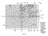
- FIG. 2 there is shown a portion 100 of the primary layer 12 of the multilayer signal routing device 10 shown in Figure 1. That is, the portion 100 shown in Figure 2 corresponds to a portion of the primary layer 12 of the multilayer signal routing device 10 where one quadrant of an electronic component having a surface mount grid array package with 1247 electrically conductive contacts is mounted on the primary layer 12 of the multilayer signal routing device 10.
- column 1 and row 1 as shown in Figure 2 correspond to an outer column and row, respectively, of the overall grid array package of the electronic component
- column 21 and row 16 as shown in Figure 2 correspond to an inner column and row, respectively, of the overall grid array package of the electronic component.
- the portion 100 comprises an array of electrically conductive contacts 102, which may be electrically connected with respective ones of the electrically conductive contacts of the electronic component.
- the portion 100 also comprises outlines for a plurality of channels 104 that may be formed in other layers (i.e., signal layers 16, power/ground layers 18, and secondary layer 14) of the multilayer signal routing device 10 using channel formation techniques as described in one or more of the above-referenced related patent applications.
- channels 104a may be formed using the microvia-based techniques as described in the above-referenced related patent applications
- channels 104b may be formed using the microvia-based techniques, power/ground-based techniques, and/or dog-bone techniques as described in the above-referenced related patent applications.
- channels 104a are shown with electrically conductive contacts 102 formed therein. These electrically conductive contacts 102 within channels 104a represent microvias that are used to enable the formation of the channels 104a using the microvia-based techniques as described in the above-referenced related patent applications. At least three of the electrically conductive contacts 102 may be arranged to form each of the at least one channel.
- channels 104b are shown without any electrically conductive contacts formed therein.
- the absence of electrically conductive contacts within channels 104b indicate that the channels 104b may be formed using the microvia-based techniques, power/ground-based techniques, and/or dog-bone techniques as described in the above-referenced related patent applications.
- each of the electrically conductive contacts 102 may have one of several different types of electrical properties (e.g., Signal, Ground (GND), Power (Vdd, Vdd2), or Test), as defined in the electrical property legend.
- each of the electrically conductive contacts 102 having a Signal electrical property is grouped into one of several catchments as indicated by the shading of those electrically conductive contacts 102. Each catchment is formed to indicate which channel 104 may be used to route signals to and from electrically conductive contacts 102 within that catchment.
- the 24 electrically conductive contacts 102 having descending (as viewed from left to right) diagonal line shading are all part of the catchment which may use the channel 104a formed in column 11, rows 1-8 to route signals to and from those 24 electrically conductive contacts 102.
- the 23 electrically conductive contacts 102 having ascending (as viewed from left to right) diagonal line shading are all part of the catchment which may use the channel 104a formed in row 8, columns 1-11 to route signals to and from those 23 electrically conductive contacts 102.
- the 23 electrically conductive contacts 102 having light gray shading are all part of the catchment which may use the channel 104a formed in row 12, columns 1-16 to route signals to and from those 23 electrically conductive contacts 102.
- the 25 electrically conductive contacts 102 having the light honeycomb shading pattern are all part of the catchment which may use the channel 104a formed in column 17, rows 1-11 to route signals to and from those 25 electrically conductive contacts 102.
- the 13 electrically conductive contacts 102 having the combined vertical and horizontal line shading are all part of the catchment which may use the channel 104b formed alongside row 16 to route signals to and from those 13 electrically conductive contacts 102. It is assumed that there are 13 additional electrically conductive contacts (not shown) formed in an adjacent quadrant (not shown) which may also use the channel 104b formed alongside row 16 to route signals to and from those 13 additional electrically conductive contacts. Similarly, it should be noted that the 11 electrically conductive contacts 102 having the dark honeycomb shading pattern are all part of the catchment which may use the channel 104b formed alongside column 21 to route signals to and from those 11 electrically conductive contacts 102.
- FIG. 3 there is shown an alternate embodiment of a portion 200 of the primary layer 12 of the multilayer signal routing device 10 shown in Figure 1.
- the alternate embodiment portion 200 shown in Figure 3 is identical to the portion 100 shown in Figure 2, except that the outermost row/column of the electrically conductive contacts 102 is staggered so as to provide greater access to the electrically conductive contacts 102 in the outer three rows/columns of the electrically conductive contacts 102 and thereby insure that signals may indeed be easily routed to and from these electrically conductive contacts 102 without the use of a channel 104.
- the staggering of the outermost row/column of the electrically conductive contacts 102 may be accomplished using the microvia-based techniques and/or power/ground-based techniques as described in the above-referenced related patent applications.
- channels 104 may be formed within the quadrant of electrically conductive contacts 102 by converting all through-hole vias (e.g., supervias 20 and 22) for a proposed channel 104 into microvias (and blind vias).
- the signals associated with these microvias must therefore all be routed on a microvia signal layer (e.g., signal layer 16a).
- the maximum number of microvias that can be routed on a microvia signal layer may be calculated by adding the number of electrically conductive signal paths that can fit between edge vias of the array with half the number of electrically conductive signal paths that can be routed in center channels (e.g., channels 104b), less between 1 and 3 vias associated with congestion effects in each corner of the array.
- the length of a single channel 104 may be calculated by subtracting the number of outermost rows/columns that are not routed in channels (e.g., 3 in Figure 2) from half of the array width, and then dividing by two plus the number of outermost rows/columns that are not routed in channels (e.g., 3 in Figure 2).
- the length of two channels 104 may be calculated by dividing the number of outermost rows/columns that are not routed in channels (e.g., 3 in Figure 2) by one third and two thirds, respectively, and then dividing by two plus the number of outermost rows/columns that are not routed in channels (e.g., 3 in Figure 2).
- the length of three channels may be calculated similar to the calculation in step 308.
- the number of channels that can be formed in the quadrant e.g., 1, 2, 3, or more channels per quadrant
- the number of microvia-associated signals that can be routed on the microvia signal layer may be determined by making sure the sum of the number of signals that need to be routed on the microvia signal layer is less than the maximum number of microvias that can be routed on the microvia signal layer.
- T represents the total number of microvias per quadrant
- A is equal to the number of electrically conductive contacts 102 in the X dimension (i.e., rows) of the full array
- B is equal to the number of electrically conductive contacts 102 in the Y dimension (i.e., columns) of the full array
- n is equal to the number of electrically conductive signal paths that may be formed between electrically conductive contacts 102.
- the (-2), (+2.5), and (+2.5) terms in the above equation represent array corner congestion and center channel constants, which indicate that 2 vias are lost due to an array corner but 2.5 vias are gained each way because of a center channel (e.g., channels 104b).
- R vias need to be converted as follows: R ⁇ 0.62 * (A+B)/2 - 2 In this case, the channel always fits.
- R vias need to be converted as follows: R ⁇ (0.7 + 0.4) * (A+B)/2 - 4 In this case, the two channels fit if 0.1*(A+B)/2 ⁇ 5 (i.e., if (A+B) ⁇ 100).
- R vias need to be converted as follows: R ⁇ (0.8 + 0.65 + 0.4) * (A+B)/2 - 6 In this case, the three channels fit if 0.85*(A+B)/2 ⁇ 7 (i.e., if (A+B) ⁇ 16).
- step 402 differential pair signals need to be located and then routed together on the same signal layer.
- step 404 bussed signals need to be located and should be routed together as a group. This makes subsequent signal routing more efficient.
- step 406 the maximum number of signals that each channel 104 supports are routed starting from vias located as far into the array and away from the channel 104 as possible. Then, after all the channels 104 have been used, signals nearest the edge of the array are routed using any remaining gaps between vias.
- step 408 if a significant number of signals need to cross the array from one side to the other, the use of center channels (e.g., channels 104b) for typical internal-to-external signal routing should be reduced, thereby leaving space in the center channels for such cross-array signal routing. Typically, the extent of this reduction depends on whether the array is associated with the largest electronic component that is mounted on the multilayer signal routing device 10, and whether an extra signal routing layer may be needed.
- step 410 the above-described steps are repeated on a subsequent signal layer until all signals are routed.
- FIG. 6 there is shown another alternate embodiment of a portion 500 of the primary layer 12 of the multilayer signal routing device 10 shown in Figure 1.
- the alternate embodiment portion 500 shown in Figure 6 is identical to the portion 100 shown in Figure 2, except that two electrically conductive contacts 102 have different electrical properties and channels 502 are formed in different locations having different shapes. More specifically, the channels 502 have diamond shapes to route around both sides of the electrically conductive contacts 102 (and corresponding vias) that have been changed to have Power (Vdd, Vdd2) electrical properties.
- the diamond-shaped channels 502 are useful for routing around electrically conductive contacts 102 (and corresponding vias) having Power (Vdd, Vdd2) and Ground (GND) electrical properties since electrically conductive contacts 102 having these electrical properties typically also have through-hole vias, which may otherwise block channels formed on signal layers (e.g., signal layers 16b, 16c, and 16d).
- FIG 7 there is shown a portion 600 of the portion 500 shown in Figure 6, wherein electrically conductive signal paths 602 are shown formed in the channels 502 that are shown in Figure 6. It should be noted that the non-shaded electrically conductive contacts 102 indicate where the channels 502 are formed on inner signal layers (e.g., signal layers 16b, 16c, and 16d) of the multilayer signal routing device 10 shown in Figure 1.
- inner signal layers e.g., signal layers 16b, 16c, and 16d
- each of the channels 502 that are shown in Figure 6 four electrically conductive signal paths 602 are shown formed in each of the channels 502 that are shown in Figure 6.
- Each of these two groups of four electrically conductive signal paths 602 are split into two groups of two electrically conductive signal paths 602 in the diamond-shaped areas of the channels 502 that are shown in Figure 6. While this is useful for routing around electrically conductive contacts 102 (and corresponding vias) having Power (Vdd, Vdd2) and Ground (GND) electrical properties as described above, the full routing capabilities of the channels 502 are not being utilized. That is, the channels 502 that are shown in Figure 6 may accommodate at least five electrically conductive signal paths in non-diamond-shaped areas thereof.
- some electrically conductive contacts 102 may be shifted in location to allow more than two electrically conductive signal paths 602 to be formed in one branch of the diamond-shaped areas of the channels 502 that are shown in Figure 6.
- FIG 8 there is shown an alternate embodiment portion 700 of the portion 500 shown in Figure 6, wherein some electrically conductive contacts 102 (i.e., those within the diamond-shaped area of the channels 502) are shifted in location to allow more than two electrically conductive signal paths 602 to be formed in one branch of the diamond-shaped areas of the channels 502 that are shown in Figure 6.
- the shifting of the locations of the electrically conductive contacts 102 (and corresponding vias) may be accomplished using the power/ground-based techniques and/or dog-bone techniques as described in the above-referenced related patent applications.
- FIG. 9 there is shown another alternate embodiment of a portion 800 of the primary layer 12 of the multilayer signal routing device 10 shown in Figure 1.
- the alternate embodiment portion 800 shown in Figure 9 is identical to the portion 100 shown in Figure 2, except that the center channels 104b are removed and groups 802 of electrically conductive contacts 102 having the Signal electrical property are formed. Expanding on step 406 of the algorithm 400 of Figure 5, the groups 802 of electrically conductive contacts 102 are formed such that they are paired together when routing signals using channels 104 and routing signals using gaps remaining between the outermost vias.
- the default method is to route the maximum number of signals that each channel 104 supports starting from vias located as far into the array and away from the channel 104 as possible. Then, after all the channels 104 have been used, signals nearest the edge of the array are routed using any remaining gaps between the outermost vias.
- inner signal layers e.g., signal layers 16b, 16c, and 16d
- signals associated with electrically conductive contacts 102 in group 802a are first routed using the channel 104a formed in column 17, rows 1-11, and then signals associated with electrically conductive contacts 102 in group 802f are routed using any remaining gaps between the outermost vias.
- signals associated with electrically conductive contacts 102 in group 802b are first routed using the channel 104a formed in column 17, rows 1-11, and then signals associated with electrically conductive contacts 102 in group 802e are routed using any remaining gaps between the outermost vias. This process continues and works well until the last inner signal layer when the proximity of the two groups (e.g., groups 802c and 802d) can cause blocking.
- first inner signal layer e.g., signal layers 16b
- signals associated with electrically conductive contacts 102 in group 802a are first routed using the channel 104a formed in column 17, rows 1-11, and then signals associated with electrically conductive contacts 102 in group 802d are routed using any remaining gaps between the outermost vias.
- signals associated with electrically conductive contacts 102 in group 802b are first routed using the channel 104a formed in column 17, rows 1-11, and then signals associated with electrically conductive contacts 102 in group 802e are routed using any remaining gaps between the outermost vias.
- This process continues and works well through the last inner signal layer because the last two groups (e.g., groups 802c and 802f) are not proximate each other and thus do not cause blocking.
- FIG 10 there is shown an alternate embodiment of a portion 900 of the primary layer 12 of the multilayer signal routing device 10 shown in Figure 1.
- the alternate embodiment portion 900 shown in Figure 10 corresponds to a portion of the primary layer 12 of the multilayer signal routing device 10 where an electronic component having a surface mount grid array package with 840 (i.e., a 29 x 29 array) electrically conductive contacts may be mounted on the primary layer 12 of the multilayer signal routing device 10.
- the portion 900 comprises 840 (i.e., also a 29 x 29 array) electrically conductive contacts 902 for mating with the 840 electrically conductive contacts of the surface mount grid array package of the electronic component that may be mounted on the primary layer 12 of the multilayer signal routing device 10.
- the 840 electrically conductive contacts 902 may mate with 840 corresponding electrically conductive contacts of multiple surface mount grid array packages of multiple electronic components (or multichip modules or hybrid modules having multiple electronic components of like or differing kind) that may be mounted on the primary layer 12 of the multilayer signal routing device 10.
- each of the electrically conductive contacts 902 may have one of several different types of electrical properties (e.g., Signal, Ground (GND, Vdd GND), Power (Vdd 1.8, Vdd 2.5, Vdd 1.5a, Vdd 1.5b), or Spare/Test), as defined in the electrical property legend.
- some of the electrically conductive contacts 902 having the Signal electrical property are grouped together as differential signal pairs 904. Because of these differential signal pair groupings 904, center channels in the array of 840 electrically conductive contacts 902 should be formed in carefully chosen areas.
- Figure 11 shows a portion 1000 (i.e., the upper half portion) of the portion 900 shown in Figure 10, wherein a center channel 1002 is formed in a poorly chosen area. More specifically, the center channel 1002 is formed in an area (i.e., between columns 13 and 14 in the upper right quadrant) such that two differential signal pair groupings 904a and 904b span the center channel 1002.
- the center channel 1002 is formed in a poorly chosen area because electrically conductive signal paths 1004 routed to/from both of the two differential signal pair groupings 904a and 904b spanning the center channel 1002 cannot be routed together, as is generally preferred. Instead, as shown in Figure 11, only the electrically conductive signal paths 1004a may be routed together to/from their respective differential signal pair grouping 904a, thereby separating the electrically conductive signal paths 1004b that are routed to/from their respective differential signal pair grouping 904b.
- FIG 10 shows both carefully and poorly chosen areas where center channels may be formed.
- carefully chosen areas 906 for forming center channels are chosen based at least in part upon minimizing the number of differential signal pair groupings 904 that will span resulting center channels.
- poorly chosen areas 908 for forming center channels are typically chosen without regard for minimizing the number of differential signal pair groupings 904 that will span resulting center channels.
- three or more differential signal pair groupings 904 will span resulting center channels based upon the poorly chosen areas 908.
- center channels may be formed and/or expanded in the array of 840 electrically conductive contacts 902 using the microvia-based techniques, power/ground-based techniques, and/or dog-bone techniques as described in the above-referenced related patent applications.
- FIG 12 there is shown a portion 1100 of an inner signal layer (e.g., signal layer 16b, 16c, or 16d) of the multilayer signal routing device 10 shown in Figure 1 corresponding to a portion (i.e., the upper right quadrant) of the portion 900 shown in Figure 10.
- the electrically conductive contacts 902 along the outer edges of the array have been staggered so as to allow for enhanced signal routing to and from electrically conductive contacts 902 in the outer rows/columns of the array, as described above.
- a plurality of electrically conductive signal paths 1102 are formed on the portion 1100 of the inner signal layer for routing signals to and from selected ones of the electrically conductive contacts 902 within the array. Notice that differential signal pair groupings 904 are routed together, as is preferred.
- channels 1104 are formed on the portion 1100 of the inner signal layer using the microvia-based techniques as described in the above-referenced related patent applications.
- Figure 12 shows how some channels (i.e., channels 1104a and 1104b) may be extended by allowing selected electrically conductive contacts 902b' having the Ground (GND) electrical property to be converted into microvias. That is, electrically conductive contacts 902 having the Power (Vdd 1.8) and Ground (GND, Vdd GND) and electrical properties are typically associated with through-hole vias, and thereby cause channel blockages.
- GND Ground
- channels (1104a and 1104b) may be extended on signal layers beneath a ground microvia layer.
- the selected electrically conductive contacts 902b' may correspond to the power/ground microvias 32
- the ground microvia layer may correspond to power/ground layer 18a
- the inner signal layers may correspond to signal layers 16a, 16b, 16c, and 16d.
- electrically conductive contacts having electrical properties that are typically associated with through-hole vias may also be converted into microvias so as to allow channels to be extended similar to above.
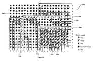
- FIG. 13 there is shown an alternate embodiment of a portion 1200 of the primary layer 12 of the multilayer signal routing device 10 shown in Figure 1.
- the alternate embodiment portion 1200 shown in Figure 13 is identical to the portion 100 shown in Figure 2, except that the center channels 104b are removed and a portion (i.e., the non-shaded electrically conductive contacts 102) of the electrically conductive contacts 102 do not represent microvias. That is, the non-shaded electrically conductive contacts 102 represent electrically conductive pads that are formed only on the primary layer 12 of the multilayer signal routing device 10 and do not extend to other layers of the multilayer signal routing device 10.
- signals may be routed to/from these non-shaded electrically conductive contacts 102 only on the primary layer 12 of the multilayer signal routing device 10 via a plurality of electrically conductive signal paths 1202 formed on the primary layer 12 of the multilayer signal routing device 10.
- the non-shaded electrically conductive contacts 102 are arranged so as to form channels 104a in other layers of the multilayer signal routing device 10.
- FIG 14 there is shown an embodiment of a portion 1300 of one of the plurality of electrically conductive signal path layers 16 of the multilayer signal routing device 10 shown in Figure 1, having channels 104a formed therein.
- the channels 104a correspond to the locations of the non-shaded electrically conductive contacts 102 formed on the primary layer 12 of the multilayer signal routing device 10. Similar to the above-mentioned embodiments, the channels 104a may be used to route signals on other layers of the multilayer signal routing device 10.
Landscapes
- Engineering & Computer Science (AREA)
- Microelectronics & Electronic Packaging (AREA)
- General Engineering & Computer Science (AREA)
- Mechanical Engineering (AREA)
- Design And Manufacture Of Integrated Circuits (AREA)
- Internal Circuitry In Semiconductor Integrated Circuit Devices (AREA)
- Production Of Multi-Layered Print Wiring Board (AREA)
Abstract
Description
wherein a
Claims (20)
- A method for reducing the number of layers in a multilayer signal routing device, the multilayer signal routing device having a plurality of electrically conductive signal path layers for routing a plurality of electrical signals thereon, the method comprising:forming a plurality of electrically conductive vias in the multilayer signal routing device for electrically connecting at least two of the plurality of electrically conductive signal path layers, the plurality of electrically conductive vias being arranged so as to form at least one channel in at least one other of the plurality of electrically conductive signal path layers; andgrouping at least a portion of the plurality of electrical signals based at least in part upon their proximity to the at least one channel so that they may be efficiently routed therein.
- The method of claim 1, wherein the at least one channel corresponds in shape to the arrangement of the plurality of electrically conductive vias.
- The method of claim 1, wherein the at least one other of the plurality of electrically conductive signal path layers is not located between the at least two electrically connected electrically conductive signal path layers.
- The method of claim 1, wherein the plurality of electrically conductive vias form a part of an array of a plurality of electrically conductive contacts, wherein at least some of the plurality of electrically conductive contacts are respectively associated with at least some of the plurality of electrical signals, wherein electrical signals that are respectively associated with electrically conductive contacts located along a perimeter of the array are not routed in the at least one channel.
- The method of claim 4, further comprising:calculating an optimum number of the at least one channel based upon at least one of: a number of electrically conductive signal paths that fit between electrically conductive contacts; a number of electrically conductive signal paths that fit within the at least one channel; a number of electrical signals that are respectively associated with electrically conductive contacts located along the perimeter of the array that are not routed in the at least one channel; and a number of electrically conductive contacts located along the perimeter of the array that are respectively associated with electrical signals that are not routed in the at least one channel.
- The method of claim 4, further comprising:subgrouping at least a portion of the grouped plurality of electrical signals based at least in part upon their proximity to the perimeter of the array.
- The method of claim 6, further comprising:routing subgroups of electrical signals located furthest from the perimeter of the array in the at least one channel.
- The method of claim 7, further comprising:routing subgroups of electrical signals located closest to the perimeter of the array in the at least one channel only after subgroups of electrical signals located furthest from the perimeter of the array have been routed.
- The method of claim 6, further comprising:routing subgroups of electrical signals located closest to the perimeter of the array outside the at least one channel.
- The method of claim 6, further comprising:pairing subgroups of electrical signals located closer to the perimeter of the array with subgroups of electrical signals located further from the perimeter of the array so as to improve routing efficiency.
- The method of claim 4, wherein the at least one channel is at least partially substantially diamond-shaped so as to allow electrical signals to be routed around electrically conductive contacts disposed within a center portion of the diamond shape.
- The method of claim 11, further comprising:shifting the locations of the electrically conductive contacts disposed within the center portion of the diamond shape so as to allow additional electrical signals to be routed around the electrically conductive contacts disposed within the center portion of the diamond shape.
- The method of claim 4, wherein the at least one channel includes a center channel formed substantially through a center of the array.
- The method of claim 13, wherein the center channel is located substantially through the center of the array based upon at least one of: a number of electrical signals identified as differential signal pairs that may span the center channel; even distribution of electrical signal routing within the center channel; even distribution of electrical signal routing within others of the at least one channel; even distribution of electrical signal routing outside the center channel; and even distribution of electrical signal routing outside others of the at least one channel.
- The method of claim 4, further comprising:forming a separate channel substantially through a center of the array, wherein the separate channel is located substantially through the center of the array based upon at least one of: a number of electrical signals identified as differential signal pairs that may span the separate channel; even distribution of electrical signal routing within the separate channel; even distribution of electrical signal routing within the at least one channel; even distribution of electrical signal routing outside the separate channel; and even distribution of electrical signal routing outside the at least one channel.
- The method of claim 1, further comprising:forming at least one additional electrically conductive via in the multilayer signal routing device for electrically connecting at least two power/ground layers of the multilayer signal routing device, the at least one additional electrically conductive via being arranged so as to form at least one additional channel in at least one other of the plurality of electrically conductive signal path layers.
- The method of claim 1, further comprising:forming at least one additional electrically conductive via in the multilayer signal routing device for electrically connecting at least two power/ground layers of the multilayer signal routing device, the at least one additional electrically conductive via being arranged so as to extend the at least one channel in at least one other of the plurality of electrically conductive signal path layers.
- The method of claim 1, wherein at least three of the plurality of electrically conductive vias are arranged to form each of the at least one channel.
- A method for reducing the number of layers in a multilayer signal routing device, the multilayer signal routing device having a plurality of electrically conductive signal path layers for routing a plurality of electrical signals thereon, the method comprising:forming a plurality of electrically conductive contacts on a first of the plurality of electrically conductive signal path layers, at least a portion of the plurality of electrically conductive pads being arranged so as to form at least one channel in at least one other of the plurality of electrically conductive signal path layers; androuting at least a portion of the plurality of electrical signals to or from at least some of the arranged plurality of electrically conductive pads on the first of the plurality of electrically conductive signal path layers.
- The method of claim 19, wherein at least three of the arranged plurality of electrically conductive pads are arranged to form each of the at least one channel.
Applications Claiming Priority (2)
| Application Number | Priority Date | Filing Date | Title |
|---|---|---|---|
| US407460 | 1982-08-12 | ||
| US10/407,460 US7069646B2 (en) | 2000-06-19 | 2003-04-07 | Techniques for reducing the number of layers in a multilayer signal routing device |
Publications (2)
| Publication Number | Publication Date |
|---|---|
| EP1467604A2 true EP1467604A2 (en) | 2004-10-13 |
| EP1467604A3 EP1467604A3 (en) | 2006-02-01 |
Family
ID=32869175
Family Applications (1)
| Application Number | Title | Priority Date | Filing Date |
|---|---|---|---|
| EP04252038A Withdrawn EP1467604A3 (en) | 2003-04-07 | 2004-04-06 | Techniques for reducing the number of layers in a multilayer signal routing device. |
Country Status (4)
| Country | Link |
|---|---|
| US (1) | US7069646B2 (en) |
| EP (1) | EP1467604A3 (en) |
| KR (1) | KR20040087876A (en) |
| CA (1) | CA2461205A1 (en) |
Families Citing this family (16)
| Publication number | Priority date | Publication date | Assignee | Title |
|---|---|---|---|---|
| TWI297095B (en) * | 2003-10-02 | 2008-05-21 | Au Optronics Corp | Bonding pad structure for a display and fabrication method thereof |
| US7307437B1 (en) * | 2005-03-24 | 2007-12-11 | Hewlett-Packard Development Company, L.P. | Arrangement with conductive pad embedment |
| US7405946B2 (en) * | 2005-05-05 | 2008-07-29 | Lsi Logic Corporation | Ball grid array assignment |
| US7365435B2 (en) * | 2005-08-10 | 2008-04-29 | Alcatel | Alternating micro-vias and throughboard vias to create PCB routing channels in BGA interconnect grid |
| US7164572B1 (en) * | 2005-09-15 | 2007-01-16 | Medtronic, Inc. | Multi-path, mono-polar co-fired hermetic electrical feedthroughs and methods of fabrication therfor |
| US8044305B2 (en) * | 2006-05-31 | 2011-10-25 | Intel Corporation | Circuit board including hybrid via structures |
| US20080025007A1 (en) * | 2006-07-27 | 2008-01-31 | Liquid Computing Corporation | Partially plated through-holes and achieving high connectivity in multilayer circuit boards using the same |
| US20080185181A1 (en) * | 2006-11-08 | 2008-08-07 | Pfeil Charles L | Alternating via fanout patterns |
| WO2008058258A2 (en) * | 2006-11-08 | 2008-05-15 | Mentor Graphics Corporation | Use of breakouts in printed circuit board designs |
| WO2008135305A1 (en) * | 2007-05-08 | 2008-11-13 | International Business Machines Corporation | Method and apparatus for scalable and programmable delay compensation for real-time synchronization signals in a multiprocessor system with individual frequency control |
| US20090180260A1 (en) * | 2008-01-10 | 2009-07-16 | Qimonda Ag | Memory module, method for manufacturing a memory module and computer system |
| US8715006B2 (en) * | 2012-06-11 | 2014-05-06 | Tyco Electronics Corporation | Circuit board having plated thru-holes and ground columns |
| US9372205B2 (en) * | 2014-01-15 | 2016-06-21 | Taiwan Semiconductor Manufacturing Co., Ltd. | Universal probe card PCB design |
| US9748168B2 (en) * | 2015-10-29 | 2017-08-29 | Nxp Usa, Inc. | Substrate with routing |
| US10199261B1 (en) | 2017-07-19 | 2019-02-05 | Globalfoundries Inc. | Via and skip via structures |
| US11412610B2 (en) * | 2020-11-04 | 2022-08-09 | Juniper Networks, Inc | Apparatus, system, and method for mitigating the swiss cheese effect in high-current circuit boards |
Family Cites Families (30)
| Publication number | Priority date | Publication date | Assignee | Title |
|---|---|---|---|---|
| US5006820A (en) * | 1989-07-03 | 1991-04-09 | Motorola, Inc. | Low reflection input configuration for integrated circuit packages |
| US5191174A (en) * | 1990-08-01 | 1993-03-02 | International Business Machines Corporation | High density circuit board and method of making same |
| JP2739726B2 (en) * | 1990-09-27 | 1998-04-15 | インターナシヨナル・ビジネス・マシーンズ・コーポレーシヨン | Multilayer printed circuit board |
| JP2966972B2 (en) * | 1991-07-05 | 1999-10-25 | 株式会社日立製作所 | Semiconductor chip carrier, module mounting the same, and electronic device incorporating the same |
| US5363280A (en) * | 1993-04-22 | 1994-11-08 | International Business Machines Corporation | Printed circuit board or card thermal mass design |
| US5544018A (en) * | 1994-04-13 | 1996-08-06 | Microelectronics And Computer Technology Corporation | Electrical interconnect device with customizeable surface layer and interwoven signal lines |
| US5784262A (en) * | 1995-11-06 | 1998-07-21 | Symbios, Inc. | Arrangement of pads and through-holes for semiconductor packages |
| US5686764A (en) * | 1996-03-20 | 1997-11-11 | Lsi Logic Corporation | Flip chip package with reduced number of package layers |
| JP3137178B2 (en) * | 1996-08-14 | 2001-02-19 | 日本電気株式会社 | Integrated circuit wiring design method and apparatus |
| JP4234205B2 (en) * | 1996-11-08 | 2009-03-04 | ダブリュ.エル.ゴア アンド アソシエイツ,インコーポレイティド | Method for reducing inductance of vias in electronic assemblies and electronic articles |
| US5855995A (en) * | 1997-02-21 | 1999-01-05 | Medtronic, Inc. | Ceramic substrate for implantable medical devices |
| US5847936A (en) * | 1997-06-20 | 1998-12-08 | Sun Microsystems, Inc. | Optimized routing scheme for an integrated circuit/printed circuit board |
| JP3466443B2 (en) * | 1997-11-19 | 2003-11-10 | 新光電気工業株式会社 | Multilayer circuit board |
| JP3380151B2 (en) * | 1997-12-22 | 2003-02-24 | 新光電気工業株式会社 | Multilayer circuit board |
| FR2782230B1 (en) | 1998-08-06 | 2000-09-08 | Bull Electronics Angers | PRINTED CIRCUITS CARD |
| US6232564B1 (en) * | 1998-10-09 | 2001-05-15 | International Business Machines Corporation | Printed wiring board wireability enhancement |
| JP2000174153A (en) * | 1998-12-01 | 2000-06-23 | Shinko Electric Ind Co Ltd | Multilayer wiring board |
| US6310398B1 (en) * | 1998-12-03 | 2001-10-30 | Walter M. Katz | Routable high-density interfaces for integrated circuit devices |
| US6181004B1 (en) * | 1999-01-22 | 2001-01-30 | Jerry D. Koontz | Digital signal processing assembly and test method |
| US6198635B1 (en) * | 1999-05-18 | 2001-03-06 | Vsli Technology, Inc. | Interconnect layout pattern for integrated circuit packages and the like |
| JP3562568B2 (en) * | 1999-07-16 | 2004-09-08 | 日本電気株式会社 | Multilayer wiring board |
| US6689634B1 (en) | 1999-09-22 | 2004-02-10 | Texas Instruments Incorporated | Modeling technique for selectively depopulating electrical contacts from a foot print of a grid array (BGA or LGA) package to increase device reliability |
| US6256769B1 (en) * | 1999-09-30 | 2001-07-03 | Unisys Corporation | Printed circuit board routing techniques |
| US6538213B1 (en) * | 2000-02-18 | 2003-03-25 | International Business Machines Corporation | High density design for organic chip carriers |
| US6388890B1 (en) * | 2000-06-19 | 2002-05-14 | Nortel Networks Limited | Technique for reducing the number of layers in a multilayer circuit board |
| US6452262B1 (en) * | 2001-02-12 | 2002-09-17 | Lsi Logic Corporation | Layout of Vdd and Vss balls in a four layer PBGA |
| US6384341B1 (en) * | 2001-04-30 | 2002-05-07 | Tyco Electronics Corporation | Differential connector footprint for a multi-layer circuit board |
| US20030043560A1 (en) * | 2001-06-15 | 2003-03-06 | Clarkson Robert Roy | Printed circuit board having a microelectronic semiconductor device mount area for trace routing therethrough |
| US6521846B1 (en) * | 2002-01-07 | 2003-02-18 | Sun Microsystems, Inc. | Method for assigning power and ground pins in array packages to enhance next level routing |
| US6812803B2 (en) * | 2002-02-05 | 2004-11-02 | Force10 Networks, Inc. | Passive transmission line equalization using circuit-board thru-holes |
-
2003
- 2003-04-07 US US10/407,460 patent/US7069646B2/en not_active Expired - Fee Related
-
2004
- 2004-03-17 CA CA002461205A patent/CA2461205A1/en not_active Abandoned
- 2004-03-30 KR KR1020040021419A patent/KR20040087876A/en not_active Withdrawn
- 2004-04-06 EP EP04252038A patent/EP1467604A3/en not_active Withdrawn
Also Published As
| Publication number | Publication date |
|---|---|
| US20040136168A1 (en) | 2004-07-15 |
| KR20040087876A (en) | 2004-10-15 |
| CA2461205A1 (en) | 2004-10-07 |
| EP1467604A3 (en) | 2006-02-01 |
| US7069646B2 (en) | 2006-07-04 |
Similar Documents
| Publication | Publication Date | Title |
|---|---|---|
| US7069646B2 (en) | Techniques for reducing the number of layers in a multilayer signal routing device | |
| US6388890B1 (en) | Technique for reducing the number of layers in a multilayer circuit board | |
| CA2422677C (en) | Technique for reducing the number of layers in a multilayer circuit board | |
| US9001486B2 (en) | Internally overlapped conditioners | |
| EP2952074B1 (en) | Pcb having offset differential signal routing | |
| US4553111A (en) | Printed circuit board maximizing areas for component utilization | |
| CA2438751C (en) | Technique for reducing the number of layers in a signal routing device | |
| EP0928029A2 (en) | Multi-layer circuit board layout | |
| EP2952073A1 (en) | Printed circuit board having orthogonal signal routing | |
| CN101673886A (en) | Improved Matched Impedance Surface Mount Technology Footprint | |
| US4535388A (en) | High density wired module | |
| EP1075026A2 (en) | Multilayer circuit board layout | |
| EP1434474A2 (en) | Technique for electrically interconnecting electrical signals between an electronic component and a multilayer signal routing device | |
| US7035082B2 (en) | Structure of multi-electrode capacitor and method for manufacturing process of the same | |
| CA2478906A1 (en) | Techniques for pin arrangements in circuit chips | |
| US7725860B1 (en) | Contact mapping using channel routing | |
| US7281326B1 (en) | Technique for routing conductive traces between a plurality of electronic components of a multilayer signal routing device | |
| JP3067385B2 (en) | Wiring structure of multilayer printed wiring board | |
| EP1461985B1 (en) | Technique for accommodating electronic components on a multilayer signal routing device | |
| HK1064253B (en) | Technique for reducing the number of layers in a multilayer circuit board | |
| HK1147641B (en) | Technique for reducing the number of layers in a signal routing device |
Legal Events
| Date | Code | Title | Description |
|---|---|---|---|
| PUAI | Public reference made under article 153(3) epc to a published international application that has entered the european phase |
Free format text: ORIGINAL CODE: 0009012 |
|
| AK | Designated contracting states |
Kind code of ref document: A2 Designated state(s): AT BE BG CH CY CZ DE DK EE ES FI FR GB GR HU IE IT LI LU MC NL PL PT RO SE SI SK TR |
|
| AX | Request for extension of the european patent |
Extension state: AL HR LT LV MK |
|
| PUAL | Search report despatched |
Free format text: ORIGINAL CODE: 0009013 |
|
| AK | Designated contracting states |
Kind code of ref document: A3 Designated state(s): AT BE BG CH CY CZ DE DK EE ES FI FR GB GR HU IE IT LI LU MC NL PL PT RO SE SI SK TR |
|
| AX | Request for extension of the european patent |
Extension state: AL HR LT LV MK |
|
| 17P | Request for examination filed |
Effective date: 20060329 |
|
| AKX | Designation fees paid |
Designated state(s): DE FR GB |
|
| STAA | Information on the status of an ep patent application or granted ep patent |
Free format text: STATUS: THE APPLICATION HAS BEEN WITHDRAWN |
|
| 18W | Application withdrawn |
Effective date: 20070309 |