EP1467488A1 - Clock generating circuit - Google Patents
Clock generating circuit Download PDFInfo
- Publication number
- EP1467488A1 EP1467488A1 EP02715752A EP02715752A EP1467488A1 EP 1467488 A1 EP1467488 A1 EP 1467488A1 EP 02715752 A EP02715752 A EP 02715752A EP 02715752 A EP02715752 A EP 02715752A EP 1467488 A1 EP1467488 A1 EP 1467488A1
- Authority
- EP
- European Patent Office
- Prior art keywords
- phase
- circuit
- reference signal
- clock
- signal
- Prior art date
- Legal status (The legal status is an assumption and is not a legal conclusion. Google has not performed a legal analysis and makes no representation as to the accuracy of the status listed.)
- Granted
Links
Images





Classifications
-
- H—ELECTRICITY
- H03—ELECTRONIC CIRCUITRY
- H03L—AUTOMATIC CONTROL, STARTING, SYNCHRONISATION OR STABILISATION OF GENERATORS OF ELECTRONIC OSCILLATIONS OR PULSES
- H03L7/00—Automatic control of frequency or phase; Synchronisation
- H03L7/06—Automatic control of frequency or phase; Synchronisation using a reference signal applied to a frequency- or phase-locked loop
- H03L7/08—Details of the phase-locked loop
- H03L7/081—Details of the phase-locked loop provided with an additional controlled phase shifter
-
- H—ELECTRICITY
- H03—ELECTRONIC CIRCUITRY
- H03L—AUTOMATIC CONTROL, STARTING, SYNCHRONISATION OR STABILISATION OF GENERATORS OF ELECTRONIC OSCILLATIONS OR PULSES
- H03L7/00—Automatic control of frequency or phase; Synchronisation
- H03L7/06—Automatic control of frequency or phase; Synchronisation using a reference signal applied to a frequency- or phase-locked loop
- H03L7/07—Automatic control of frequency or phase; Synchronisation using a reference signal applied to a frequency- or phase-locked loop using several loops, e.g. for redundant clock signal generation
-
- H—ELECTRICITY
- H03—ELECTRONIC CIRCUITRY
- H03L—AUTOMATIC CONTROL, STARTING, SYNCHRONISATION OR STABILISATION OF GENERATORS OF ELECTRONIC OSCILLATIONS OR PULSES
- H03L7/00—Automatic control of frequency or phase; Synchronisation
- H03L7/06—Automatic control of frequency or phase; Synchronisation using a reference signal applied to a frequency- or phase-locked loop
- H03L7/08—Details of the phase-locked loop
- H03L7/081—Details of the phase-locked loop provided with an additional controlled phase shifter
- H03L7/0812—Details of the phase-locked loop provided with an additional controlled phase shifter and where no voltage or current controlled oscillator is used
- H03L7/0814—Details of the phase-locked loop provided with an additional controlled phase shifter and where no voltage or current controlled oscillator is used the phase shifting device being digitally controlled
-
- H—ELECTRICITY
- H03—ELECTRONIC CIRCUITRY
- H03L—AUTOMATIC CONTROL, STARTING, SYNCHRONISATION OR STABILISATION OF GENERATORS OF ELECTRONIC OSCILLATIONS OR PULSES
- H03L7/00—Automatic control of frequency or phase; Synchronisation
- H03L7/06—Automatic control of frequency or phase; Synchronisation using a reference signal applied to a frequency- or phase-locked loop
- H03L7/08—Details of the phase-locked loop
- H03L7/085—Details of the phase-locked loop concerning mainly the frequency- or phase-detection arrangement including the filtering or amplification of its output signal
- H03L7/087—Details of the phase-locked loop concerning mainly the frequency- or phase-detection arrangement including the filtering or amplification of its output signal using at least two phase detectors or a frequency and phase detector in the loop
Definitions
- This invention relates to a clock generation circuit, which generates a clock that is synchronized with a reference signal in a digital transmission system.
- Fig. 9 is the block diagram of a conventional clock generation circuit as an example.
- a reference numeral 1 denotes a reference signal
- a reference numeral 3 denotes a selection signal selecting one of a plurality of reference signals
- a reference numeral 4 denotes a selection circuit
- a reference numeral 5 denotes a PLL circuit
- a reference numeral 6 denotes a generated clock.
- the PLL circuit is configured with the following elements.
- a reference numeral 21 denotes a phase comparator
- a reference numeral 22 denotes a low-pass filter
- a reference numeral 23 denotes an amplifier
- a reference numeral 24 denotes a reference voltage generator
- a reference numeral 25 denotes a voltage control oscillator
- a reference numeral 26 denotes a divider.
- a plurality of reference signals 1 are inputted, and one of the plurality of reference signals is selected in the selection circuit 4 based on the selection signal 3.
- Fig. 9 shows the case of inputting two reference signals 1a and 1b for explanation.
- the phase comparator 21 outputs a signal corresponding to a phase difference between the selected reference signal and the output signal from the divider 26.
- This phase difference signal is smoothed through the low-pass filter 22, and a voltage potential difference between this signal and the reference voltage generator 24 is amplified in the amplifier 23.
- the output voltage of the amplifier 23 activates the voltage control oscillator 25 to output the clock signal 6 whose phase is synchronized with the phase of the selected reference signal 1.
- the divider 26 divides the generated clock 6 to generate the signal whose phase is to be compared with the phase of the reference signal 1.
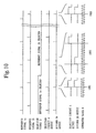
- Fig. 10 shows the reference signals 1, an output from the selection circuit 4 that is selected based on the selection signal 3, the generated clock 6, and an output signal from the divider 26.
- a reference signal 1a is selected in the selection circuit 4 based on the selection signal 3, and the divider 26 and the generated clock 6 are both synchronized with the reference signal 1a.
- a reference signal 1b is selected upon change of the selection in the selection circuit 4 based on the selection signal 3.
- the generated clock 6 and the output of the divider 26 are both out of phase with the reference signal 1b just selected.
- the phase comparator 21 outputs a phase difference signal in commensurate with this phase difference.
- the phase difference signal is then smoothed through the low-pass filter 22, and amplified through the amplifier 23 to control the transmission frequency of the voltage control oscillator 25 so that the phase of the output of the divider 26 and the phase of the reference signal 1b selected in the selection circuit 4 match.
- phase difference between the selected reference signal 1 and the generated clock 6 is called steady-state phase difference.
- the phase difference may be reduced by increasing the loop gain of the PLL circuit 5.
- the problem is that the transient phase fluctuation of the generated clock 6 gets large because it is affected by the change in phase of the reference signal 1 upon change of the reference signal 1.
- the steady-state phase difference and the size of the phase fluctuation of the generated clock 6 upon change of the reference signal 1.
- the low-pass filter 22 for enhancing filter precision performance because the low-pass filter 22 is generally configured with such as a resistance and a capacitor.
- the voltage control oscillator 25 there is VCXO (Voltage Controlled Xtal Oscillator) using crystal or VCO (Voltage Controlled Oscillator) using coils and capacitors. It is difficult to integrate VCXO. With VCO, its modulation sensitivity is so high that loop gain gets high in the PLL circuit. Therefore, the problem is that the phase fluctuation of the generated clock becomes large upon change of the reference signal.
- the conventional clock generation circuit needs to control the reference voltage generator for matching the phase of the reference signal and the phase of the generated clock. And there is a problem that it is difficult to integrate the low-pass filter or the voltage control oscillator in the case of high precision control of the steady-state phase difference or the transient response upon change of the reference signal. Still another problem is that the transient response upon change of the reference signal depends upon loop gain in the PLL circuit and the time constant of the low-pass filter, so that high design flexibility cannot be achieved.
- the present invention is directed to solving the problems discussed above. It is an object to eliminate control involved to match the phase of the reference signal and the phase of the generated clock, make it possible to integrate all the circuit elements, enable high precision transient response control upon change of the reference signal, and achieve high design flexibility.
- a clock generation circuit selects one of a plurality of reference signals and generates a clock that is synchronized with a selected reference signal.
- the clock generation circuit is characterized by including,
- the clock generation circuit is characterized by further including a plurality of phase control circuits, respectively which is provided for each of the outputs from the plurality of former stage PLL circuits for matching phase of an output from another one of the plurality of former stage PLL circuits with the phase of an output from one of the plurality of former stage PLL circuits corresponding to the selected reference signal.
- the phase control circuits are characterized by including aring counter and a selection circuit selecting one of multiphase outputs from the ring counter.
- Thepluralityof former stage PLL circuits is characterized by respectively performing synchronization in frequency with a corresponding reference signal, respectively.
- the latter stage PLL circuit is characterized by performing synchronization in phase with the selected reference signal.
- the clock generation circuit is characterized by further including a plurality of phase control circuits respectively provided for each of the outputs from the plurality of former stage PLL circuits, and controlling a phase control circuit corresponding to the selected reference signal such that the phase of a signal obtained by dividing the generated clock matches the phase of the selected reference signal.
- the plurality of phase control circuits are characterized by matching the phase of an output from another one of the plurality of former stage PLL circuits with the phase of an output from one of the plurality of former stage PLL circuits corresponding to the selected reference signal.
- the clock generation circuit is characterized by controlling the phase control circuit in commensurate with a cycle of the selected reference signal.
- the clock generation circuit is characterized by controlling the phase control circuit in commensurate with a dividing cycle of the generated clock.
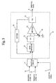
- a reference numeral 1 denotes a reference signal
- a reference numeral 2 denotes a PLL circuit
- a reference numeral 3 denotes a selection signal
- a reference numeral 4 denotes a selection circuit
- a reference numeral 5 denotes a PLL circuit
- a reference numeral 6 denotes a generated clock.
- Fig. 2 shows the waveform of each element in Fig. 1.
- the reference signals 1 are inputted, respectively, to the PLL circuits 2. More specifically, a reference signal 1a is inputted to a PLL circuit 2a, and a reference signal 1b is inputted to a PLL circuit 2b.
- the PLL circuits 2a and 2b output primary clocks that are synchronized, respectively, with the reference signals 1a and 1b inputted.
- the selection circuit 4 selects one of the primary clocks that are synchronized with the reference signals outputted from the PLL circuits 2, respectively, based on the selection signal 3.
- a selected primary clock is inputted to the PLL circuit 5 provided in the next stage .
- the PLL circuit5 outputs the generated clock 6 that is synchronized with the selected primary clock.
- Reference numerals 201 and 202 in Fig. 2 each show the waveform of each element in the case where the reference signal 1a is selected based on the selection signal 3.
- 201 in Fig. 2 it is illustrated that an output from the PLL circuit 2a is synchronized with the reference signal 1a, an output from the PLL circuit 2b is synchronized with the reference signal 1b, and the reference signal 1a is selected in the selection circuit 4 based on the selection signal 3. Consequently, the phase of the generated clock 6 is synchronized with the phase of the reference signal 1a.
- the reference signal 1a is selected based on the selection signal 3 in the selection circuit 4. Therefore, the phase of the generated clock 6 is not synchronized with the phase of the reference signal 1b.
- 203 in Fig. 2 shows the waveform of each element just after the reference signal was changed to the reference signal 1b in the selection circuit 4 based on the selection signal 3.
- the output of the selection circuit 4 is synchronized with the reference signal 1b, but the PLL circuit 5 is in a transient state to synchronization with the reference signal 1b just changed, and the generated clock 6 is not synchronized with the reference signal 1b yet.
- the waveform of each element in steady state is shown with time.
- the phase of the generated clock 6 is synchronized with the phase of the reference signal 1b selected in the selection circuit 4 based on the selection signal 3.
- the PLL circuits 2 are provided for the reference signals 1, respectively, and generate the primary clocks that are synchronized with the respective reference signals 1. Then, one of the primary clocks is selected and inputted to the PLL circuit 5 in the next stage to obtain the generated clock 6.
- phase difference between the reference signals 1 before and after the change is inputted directly to the PLL circuit 5 generating the clock. According to this embodiment, however, phase difference between the primary clocks before and after the change, which are outputted from the PLL circuits 2, is inputted to the PLL circuit 5 generating the clock. As shown in Fig.
- the PLL circuits 2 are thus provided for the reference signals 1, respectively. This further contributes to eliminating phase jitter with the input signal in each PLL circuit 2 upon change of the input signal. Accordingly, with respect to the problem of the setup of loop gain in the PLL circuit, which is trade-off with the transient response by the phase jitter of the input signal, in the conventional art, the present invention allows high loop gain setting in the PLL circuit 2. This can eliminate the phase control that is essential in the conventional art. Likewise, in the PLL circuit 5, the phase jitter of the input signal is greatly reduced, so that high loop gain may be obtained, thus eliminating phase control.
- phase jitter of the input signal thus greatly reduced in both the PLL circuit 2 and the PLL circuit 5 contributes not only to allowing high loop gain setting, but also to allowing a reduction in the precision of transient response control. Consequently, it becomes possible to integrate the voltage control oscillator 25 or the low-pass filter 22, thus allowing apparatuses to be downsized and energy consumption to be lowered.
- two types of the reference signals 1 are inputted, as an example.
- the present invention is applicable to another case in which more than two types of the reference signals 1 are to be inputted.
- two stages of the PLL circuits are linked in sequence here as an example. It is also applicable, other than this example, that more than two stages of the PLL circuits are linked in sequence.
- a reference numeral 1 denotes a reference signal
- a reference numeral 2 denotes a PLL circuit (former stage)
- a reference numeral 3 denotes a selection signal
- a reference numeral 4 denotes a selection circuit
- a reference numeral 5 denotes a PLL circuit (latter stage)
- a reference numeral 6 denotes a generated clock
- a reference numeral 7 denotes a phase control circuit
- a reference numeral 8 denotes a phase comparator circuit
- a reference numeral 9 denotes a control circuit.
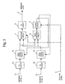
- the phase control circuits 7 are provided, respectively, at the outputs of the PLL circuits 2 receiving the reference signals 1, so that the phase of the primary clock outputted from the phase control circuit 7 through the PLL circuit 2 corresponding to the reference signal 1 selected in the selection circuit 4 based on the selection signal 3 and the phase of the primary clock outputted from the phase control circuit 7 through the PLL circuit 2 corresponding to the other reference signal 1 match.
- the phase of the primary clock that is selected and the phase of the other primary clock are compared in the phase comparator circuit 8.
- the control circuit 9 controls the phase control circuit that outputs the primary clock that is not selected so that the phases of the both primary clocks match.
- phase of the primary clock that is not selected is controlled to match the phase of the primary clock that is selected. Consequently, no phase jitter occurs in the input signal that is inputted to the PLL circuit 5 upon change in the selection circuit 4 based on the selection signal 3. This may provide more stable clocks, in addition to the benefits of integration and elimination of control that are discussed in the first embodiment
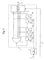
- the phase control circuit 7 discussed in the second embodiment is implemented by a ring counter and a selection circuit.
- a reference numeral 1 denotes a reference signal
- a reference numeral 2 denotes a PLL circuit (former stage)
- a reference numeral 7 denotes a phase control circuit
- a reference numeral 10 denotes flip-flops
- a reference numeral 11 denotes a NOR circuit
- a reference numeral 12 denotes a selection circuit
- a reference numeral 13 denotes a control signal
- a reference numeral 14 denotes an output of the phase control circuit.
- Fig. 5 shows the waveform of each element in Fig. 4.
- the primary clock outputted from the PLL circuit 2 operates a ring counter that is configured with flip-flops 10 and the NOR circuit 11.
- outputs from a flip-flop 10a ⁇ a flip-flop 10y are multi-phase signals depending upon the number of the stages in the ring counter. Selecting one of the multi-phase signals by using the selection circuit 12, configures the phase control circuit 7.
- the outputs from the flip-flop 10a ⁇ the flip-flop 10y are cyclic. In the phase control operation, if it is needed to control phase to delay further while the output of the flip-flop 10y is selected by the selection circuit 12, the output of the flip-flop 10a is to be selected by the selection circuit 12.
- the outputs of the flip-flops 10 which is selected by the selection circuit 12 is to be selected by cyclically. This can make the range of phase control infinite in the phase control circuit 7.
- the number of the flip-flops 10 making up the ring counter in the phase control circuit 7 is determined in combination with the speed of the primary clock outputted from the PLL circuit 2. More specifically, the number of stages of the flip-flops 10 is determined as resolution that is necessary for phase control so that no phase jitter occurs in the generated clock 6 that is outputted from the PLL circuit 5 upon change in the selection circuit 4.
- phase control circuit 7 thus configured allows the range of phase control to become infinite, thus allowing control resolution for phase control to be set freely.
- frequency-synchronization is carried out with the reference signals in the PLL circuits 2 provided for the respective reference signals 1 as discussed in the first embodiment, one of the frequency-synchronized signals is selected in the selection circuit 4, the selected signal is then inputted to the PLL circuit 5 in the next stage, and phase-synchronization is carried out with the selected reference signal 1 in the PLL circuit 5 in the next stage.
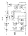
- a reference numeral 1 denotes a reference signal
- a reference numeral 2 denotes a PLL circuit ( former stage)
- a reference numeral 3 denotes a selection signal
- a reference numeral 4 denotes a selection circuit
- a reference numeral 5 denotes a PLL circuit (latter stage)
- a reference numeral 6 denotes a generated clock
- a reference numeral 7 denotes a phase control circuit
- a reference numeral 8 denotes a phase comparator circuit
- a reference numeral 9 denotes a control circuit
- a reference numeral 15 denotes a selection circuit
- a reference numeral 16 denotes a phase comparator circuit
- a reference numeral 17 denotes a control circuit
- a reference numeral 18 denotes a divider circuit
- a reference numeral 19 denotes a selection circuit
- a reference numeral 20 denotes a selection circuit.
- Incoming reference signals 1 are inputted, respectively, to the PLL circuits 2.
- the PLL circuits 2 output the primary clocks that are synchronized in frequency with the respective reference signals 1 inputted.
- the primary clocks are inputted to the selection circuit 4 through the respective phase control circuits 7. Then, one of the inputted primary clocks is selected based on the selection signal 3 and fed into the PLL circuit 5. Then, the generated clock 6 is outputted from the PLL circuit 5.
- the reference signals 1 are also inputted to the selection circuit 15, and one of the reference signals 1 is selected based on the selection signal 3.
- the selection circuit15 and the selection circuit4 select the same type of reference signal 1 and synchronized primary clock in frequency.
- the phase comparator circuit 16 compares the phase of the reference signal 1 selected in the selection circuit 15 and the phase of a signal obtained by dividing the generated clock 6 through the divider circuit 18. A result of phase comparison is inputted to the control circuit 17 and used to control the phase control circuit 7 corresponding to the selected reference signal 1.
- the phase control circuit 7 matches the phase of the reference signal 1 and the phase of the divided signal outputted from the divider circuit 18.
- the phase comparator circuit 8 compares the phase of the primary clock outputted from the PLL circuit 2 receiving the selected reference signal 1 and the phase of the primary clock outputted from the PLL circuit 2 receiving the other reference signal 1. A result of phase comparison is inputted to the control circuit 9 and used to control the phase control circuit 7 corresponding to the selected reference signal 1.
- the phase control circuit 7 matches the phase of the primary clock corresponding to the selected reference signal 1 and the phase of the primary clock corresponding to the other reference signal 1.
- the selection circuit 19 and the selection circuit 20 select the control of the phase control circuit 7 corresponding to the selected reference signal 1 and the control of the phase control circuit 7 corresponding to the other reference signal 1, respectively, based on the selection signal 3.
- the PLL circuit 2 in the first stage carries out frequency-synchronization with the reference signal 1
- the PLL circuit 5 in the next stage carries out phase -synchronization with the selected reference signal 1.
- This not only allows providing the system with the generated clock 6 whose frequency is synchronized with the selected reference signal 1 but also allows reproducing the phase that matches the selected reference signal 1.
- This is applicable to frame phase signal, for example.
- the phase of the primary clock corresponding to the selected reference signal 1 matches the phase of the primary clock corresponding to the other reference signal 1. This causes no phase jitter in the signal inputted to the PLL circuit 5 upon change of the reference signal 1 in the selection circuit 4 based on the selection signal 3.
- stable clocks may be provided.
- control circuit 17 and the control circuit 9 for controlling the phase control circuits 7 of the fourth embodiment are controlled in commensurate with the cycle of the selected reference signal 1.
- a reference numeral 1 denotes a reference signal
- a reference numeral 2 denotes a PLL circuit (former stage)
- a reference numeral 3 denotes a selection signal
- a reference numeral 4 denotes a selection circuit
- a reference numeral 5 denotes a PLL circuit (latter stage)
- a reference numeral 6 denotes a generated clock
- a reference numeral 7 denotes a phase control circuit
- a reference numeral 8 denotes a phase comparator circuit
- a reference numeral 9 denotes a control circuit
- a reference numeral 15 denotes a selection circuit
- a reference numeral 16 denotes a phase comparator circuit
- a reference numeral 17 denotes a control circuit
- a reference numeral 18 denotes a divider circuit
- a reference numeral 19 denotes a selection circuit
- a reference numeral 20 denotes a selection circuit.
- Control cycle determines the transient response upon change of the reference signal 1 to be selected based on the selection signal 3.
- the transient response is controlled based on the frequency characteristic of the low-pass filter
- high precision control is allowed according to the fifth embodiment.
- the possibility of the frequency response of the low-pass filter restricts the design flexibility of the transient response upon change of the reference signal 1 according to the conventional art.
- the control is based on logic circuit processing, and therefore there is the advantage of high design flexibility.
- control circuit 17 and the control circuit 9 for controlling the phase control circuits 7 of the fourth embodiment are controlled in commensurate with the cycle of a signal obtained by dividing the generated clock 6 in the divider circuit 18.
- a reference numeral 1 denotes a reference signal
- a reference numeral 2 denotes a PLL circuit ( former stage)
- a reference numeral 3 denotes a selection signal
- a reference numeral 4 denotes a selection circuit
- a reference numeral 5 denotes a PLL circuit (latter stage)
- a reference numeral 6 denotes a generated clock
- a reference numeral 7 denotes a phase control circuit
- a reference numeral 8 denotes a phase comparator circuit
- a reference numeral 9 denotes a control circuit
- a reference numeral 15 denotes a selection circuit
- a reference numeral 16 denotes a phase comparator circuit
- a reference numeral 17 denotes a control circuit
- a reference numeral 18 denotes a divider circuit
- a reference numeral 19 denotes a selection circuit
- a reference numeral 20 denotes a selection circuit.
- Control cycle determines the transient response upon change of the reference signal 1 to be selected based on the selection signal 3.
- the transient response is controlled based on the frequency characteristic of the low-pass filter
- high precision control is allowed according to the sixth embodiment.
- the possibility of the frequency response of the low-pass filter restricts the design flexibility of the transient response upon change of the reference signal 1 according to the conventional art.
- the control is based on logic circuit processing, and therefore there is the advantage of high design flexibility.
- the clock generation circuit is thus configured with the multiple stages of the PLL circuits, which are linked in sequence, such that the PLL circuits are provided for incoming reference signals, respectively, and one of the outputs of the PLL circuits receiving the respective reference signals is selected to be fed to the PLL circuit in the next stage.
- the phase control circuits are thus provided at the outputs of the PLL circuits provided for the respective reference signals, so that the phase of the output of the PLL circuit receiving the selected reference signal and the phase of the output of the PLL circuit receiving the other reference signal match through the phase control circuit.
- the phase control circuit is configured with the ring counter and the selection circuit selecting one of the multiphase outputs of the ring counter.
- phase control circuits are controlled in commensurate with the cycle of the reference signal or the generated clock signal.
- the configuration of PLL circuits 2 provided respectively for the reference signals 1 allows no phase jitter of the input signal upon change in the PLL circuit 2.
- the loop gain of the PLL circuit 2 is allowed to be set high according to this invention, This can eliminate the phase control that is indispensable in the conventional art.
- the phase jitter of the input signal is reduced greatly, high loop gain may be obtained, hence, the phase control may be eliminated.
- phase of the primary clock that is not selected is controlled to match the phase of the primary clock that is selected. Consequently, no phase jitter occurs in the input signal that is inputted to the PLL circuit 5 upon change in the selection circuit 4 based on the selection signal 3. This may provide more stable clocks, in addition to the benefits of integration and elimination of control that are discussed in the first embodiment
- phase control circuit 7 thus configured allows the range of phase control to become infinite, thus allowing control resolution for phase control to be set freely.
- the PLL circuit 2 in the first stage carries out frequency-synchronization with the reference signal 1, and the PLL circuit 5 in the next stage carries out phase -synchronization with the selected reference signal 1.
- This not only allows providing the system with the generated clock 6 whose frequency is synchronized with the selected reference signal 1 but also allows reproducing the phase that matches the selected reference signal 1.
- This is applicable to frame phase signal, for example.
- the phase of the primary clock corresponding to the selected reference signal 1 matches the phase of the primary clock corresponding to the other reference signal 1. This causes no phase jitter in the signal inputted to the PLL circuit 5 upon change of the reference signal 1 in the selection circuit 4 based on the selection signal 3.
- stable clocks may be provided.
- the control is based on logic circuit processing, and therefore there is the advantage of high design flexibility.
- the control is based on logic circuit processing, and therefore there is the advantage of high design flexibility.
Landscapes
- Stabilization Of Oscillater, Synchronisation, Frequency Synthesizers (AREA)
Abstract
Description
Claims (6)
- A clock generation circuit, which selects one of a plurality of reference signals and generates a clock that is synchronized with a selected reference signal, the clock generation circuit comprising:(1) a plurality of former stage PLL circuits respectively provided for each of the plurality of reference signals, generating outputs that are respectively synchronized with a corresponding reference signal;(2) a selection circuit selecting one of the outputs from the plurality of former stage PLL circuits; and(3) a latter stage PLL circuit linked in sequence to the plurality of former stage PLL circuits, for receiving the one of the outputs selected and generating the clock.
- The clock generation circuit according to claim 1, further comprising a plurality of phase control circuits, respectively provided for each of the outputs from the plurality of former stage PLL circuits, for matching phase of an output from another one of the plurality of former stage PLL circuits with phase of an output from one of the plurality of former stage PLL circuits corresponding to the selected reference signal.
- The clock generation circuit according to claim 2, wherein the phase control circuits includes a ring counter and a selection circuit selecting one of multiphase outputs from the ring counter.
- The clock generation circuit according to claim 1, wherein the plurality of former stage PLL circuits respectively perform synchronization in frequency with a corresponding reference signal, respectively, and
wherein the latter stage PLL circuit performs synchronization in phase with the selected reference signal,
the clock generation circuit further comprising,
a plurality of phase control circuits respectively provided for each of the outputs from the plurality of former stage PLL circuits,
wherein the clock generation circuit controls a phase control circuit corresponding to the selected reference signal such that phase of a signal obtained by dividing the generated clock matches phase of the selected reference signal, and
wherein the plurality of phase control circuits matchphase of an output from another one of the plurality of former stage PLL circuits with phase of an output from one of the plurality of former stage PLL circuits corresponding to the selected reference signal. - The clock generation circuit according to claim 4, wherein the clock generation circuit controls the phase control circuit in commensurate with a cycle of the selected reference signal.
- The clock generation circuit according to claim 4, wherein the clock generation circuit controls the phase control circuit in commensurate with a dividing cycle of the generated clock.
Applications Claiming Priority (1)
| Application Number | Priority Date | Filing Date | Title |
|---|---|---|---|
| PCT/JP2002/000233 WO2003061129A1 (en) | 2002-01-16 | 2002-01-16 | Clock generating circuit |
Publications (3)
| Publication Number | Publication Date |
|---|---|
| EP1467488A1 true EP1467488A1 (en) | 2004-10-13 |
| EP1467488A4 EP1467488A4 (en) | 2005-04-27 |
| EP1467488B1 EP1467488B1 (en) | 2007-04-11 |
Family
ID=11738130
Family Applications (1)
| Application Number | Title | Priority Date | Filing Date |
|---|---|---|---|
| EP02715752A Expired - Lifetime EP1467488B1 (en) | 2002-01-16 | 2002-01-16 | Clock generating circuit |
Country Status (5)
| Country | Link |
|---|---|
| US (1) | US7088155B2 (en) |
| EP (1) | EP1467488B1 (en) |
| JP (1) | JP3810408B2 (en) |
| DE (1) | DE60219527T8 (en) |
| WO (1) | WO2003061129A1 (en) |
Cited By (5)
| Publication number | Priority date | Publication date | Assignee | Title |
|---|---|---|---|---|
| WO2009134880A1 (en) | 2008-04-29 | 2009-11-05 | Qualcomm Incorporated | System and method of controlling power consumption in a digital phase locked loop (dpll) |
| WO2010056814A1 (en) * | 2008-11-14 | 2010-05-20 | Analog Devices, Inc. | Multiple input pll with hitless switchover between non-integer related input frequencies |
| US7924072B2 (en) | 2008-11-14 | 2011-04-12 | Analog Devices, Inc. | Exact frequency translation using dual cascaded sigma-delta modulator controlled phase lock loops |
| US7924966B2 (en) | 2008-11-21 | 2011-04-12 | Analog Devices, Inc. | Symmetry corrected high frequency digital divider |
| US8223806B2 (en) | 2007-09-07 | 2012-07-17 | Thomson Licensing | Reduction in the acquisition duration of a phase-locked loop able to reconstitute a synchronisation signal transmitted over an IP network |
Families Citing this family (17)
| Publication number | Priority date | Publication date | Assignee | Title |
|---|---|---|---|---|
| WO2004021636A1 (en) * | 2002-08-30 | 2004-03-11 | Telefonaktiebolaget Lm Ericsson (Publ). | Method and arrangement for reducing phase jumps when switching between synchronisation sources |
| KR100533915B1 (en) * | 2003-10-21 | 2005-12-06 | 한국전자통신연구원 | Clock signal selecting device and method for guaranting its clock continuity |
| US7747237B2 (en) * | 2004-04-09 | 2010-06-29 | Skyworks Solutions, Inc. | High agility frequency synthesizer phase-locked loop |
| US7522690B2 (en) * | 2004-09-15 | 2009-04-21 | Silicon Laboratories Inc. | Jitter self test |
| TWI316793B (en) * | 2006-06-28 | 2009-11-01 | Realtek Semiconductor Corp | Frequency synthesizer with a plurality of frequency locking circuits |
| KR100815187B1 (en) * | 2006-08-31 | 2008-03-19 | 주식회사 하이닉스반도체 | Semiconductor memory device |
| TWI332318B (en) * | 2006-09-07 | 2010-10-21 | Realtek Semiconductor Corp | Multiloop phase locked loop circuit |
| TWI427458B (en) * | 2006-11-30 | 2014-02-21 | Semiconductor Energy Lab | Clock generating circuit and semiconductor device provided with clock generating circuit |
| KR100955675B1 (en) * | 2007-08-23 | 2010-05-06 | 주식회사 하이닉스반도체 | Clock pulse generation circuit |
| US7902886B2 (en) * | 2007-10-30 | 2011-03-08 | Diablo Technologies Inc. | Multiple reference phase locked loop |
| JP2010074201A (en) * | 2008-09-16 | 2010-04-02 | Nec Electronics Corp | Synchronization detection circuit, pulse width modulation circuit using the same and synchronization detection method |
| US20140035635A1 (en) * | 2011-03-23 | 2014-02-06 | Tejas Networks Limited Plot No. 25, JP Software Park | Apparatus for glitch-free clock switching and a method thereof |
| CN208337594U (en) * | 2018-06-21 | 2019-01-04 | 新港海岸(北京)科技有限公司 | A kind of clock lossless switching system |
| US10541689B1 (en) * | 2018-07-06 | 2020-01-21 | M31 Technology Corporation | Clock generation circuit and associated circuitry |
| US10623174B1 (en) * | 2018-12-12 | 2020-04-14 | Xilinx, Inc. | Low latency data transfer technique for mesochronous divided clocks |
| JP7393079B2 (en) * | 2019-03-26 | 2023-12-06 | ラピスセミコンダクタ株式会社 | semiconductor equipment |
| US11039517B2 (en) * | 2019-04-01 | 2021-06-15 | Sct Ltd. | Fraction PWM with multiple phase display clock |
Family Cites Families (13)
| Publication number | Priority date | Publication date | Assignee | Title |
|---|---|---|---|---|
| JPH04113718A (en) | 1990-09-04 | 1992-04-15 | Fujitsu Ltd | Hitless clock switching device |
| JPH06232739A (en) | 1993-02-05 | 1994-08-19 | Toshiba Corp | Clock redundancy method |
| JP3036402B2 (en) | 1994-05-18 | 2000-04-24 | 日本電気株式会社 | PLL controller |
| JPH0818447A (en) | 1994-06-28 | 1996-01-19 | Mitsubishi Electric Corp | PLL circuit device |
| US5748569A (en) * | 1996-12-19 | 1998-05-05 | Dsc Telecom L.P. | Apparatus and method for clock alignment and switching |
| JPH10290158A (en) | 1997-04-15 | 1998-10-27 | Saitama Nippon Denki Kk | Duplicate phase synchronization device |
| JP3720996B2 (en) | 1998-02-27 | 2005-11-30 | 株式会社東芝 | Clock switching device |
| JP3132657B2 (en) | 1998-04-15 | 2001-02-05 | 日本電気株式会社 | Clock switching circuit |
| JP2000148281A (en) | 1998-11-12 | 2000-05-26 | Nec Commun Syst Ltd | Clock selection circuit |
| JP2001077690A (en) | 1999-09-06 | 2001-03-23 | Matsushita Electric Ind Co Ltd | Clock supply apparatus and method |
| JP2001251182A (en) | 1999-12-28 | 2001-09-14 | Sony Corp | Reference wave switching device and communication device, and digital broadcasting system and method |
| GB2363268B (en) * | 2000-06-08 | 2004-04-14 | Mitel Corp | Timing circuit with dual phase locked loops |
| JP3531630B2 (en) * | 2001-08-07 | 2004-05-31 | 日本電気株式会社 | Clock generation circuit |
-
2002
- 2002-01-16 DE DE60219527T patent/DE60219527T8/en active Active
- 2002-01-16 WO PCT/JP2002/000233 patent/WO2003061129A1/en not_active Ceased
- 2002-01-16 US US10/500,717 patent/US7088155B2/en not_active Expired - Fee Related
- 2002-01-16 EP EP02715752A patent/EP1467488B1/en not_active Expired - Lifetime
- 2002-01-16 JP JP2003561098A patent/JP3810408B2/en not_active Expired - Fee Related
Cited By (11)
| Publication number | Priority date | Publication date | Assignee | Title |
|---|---|---|---|---|
| US8223806B2 (en) | 2007-09-07 | 2012-07-17 | Thomson Licensing | Reduction in the acquisition duration of a phase-locked loop able to reconstitute a synchronisation signal transmitted over an IP network |
| WO2009134880A1 (en) | 2008-04-29 | 2009-11-05 | Qualcomm Incorporated | System and method of controlling power consumption in a digital phase locked loop (dpll) |
| CN102017418A (en) * | 2008-04-29 | 2011-04-13 | 高通股份有限公司 | Systems and methods for controlling power consumption in a digital phase locked loop (DPLL) |
| US8077822B2 (en) | 2008-04-29 | 2011-12-13 | Qualcomm Incorporated | System and method of controlling power consumption in a digital phase locked loop (DPLL) |
| CN106160741A (en) * | 2008-04-29 | 2016-11-23 | 高通股份有限公司 | The system and method for the power consumption in control digital phase-locked loop (DPLL) |
| CN102017418B (en) * | 2008-04-29 | 2018-06-12 | 高通股份有限公司 | Systems and methods for controlling power consumption in a digital phase locked loop (DPLL) |
| CN106160741B (en) * | 2008-04-29 | 2019-08-13 | 高通股份有限公司 | The system and method for controlling the power consumption in digital phase-locked loop (DPLL) |
| WO2010056814A1 (en) * | 2008-11-14 | 2010-05-20 | Analog Devices, Inc. | Multiple input pll with hitless switchover between non-integer related input frequencies |
| US7893736B2 (en) | 2008-11-14 | 2011-02-22 | Analog Devices, Inc. | Multiple input PLL with hitless switchover between non-integer related input frequencies |
| US7924072B2 (en) | 2008-11-14 | 2011-04-12 | Analog Devices, Inc. | Exact frequency translation using dual cascaded sigma-delta modulator controlled phase lock loops |
| US7924966B2 (en) | 2008-11-21 | 2011-04-12 | Analog Devices, Inc. | Symmetry corrected high frequency digital divider |
Also Published As
| Publication number | Publication date |
|---|---|
| EP1467488A4 (en) | 2005-04-27 |
| US20050062505A1 (en) | 2005-03-24 |
| EP1467488B1 (en) | 2007-04-11 |
| DE60219527T2 (en) | 2007-12-27 |
| WO2003061129A1 (en) | 2003-07-24 |
| DE60219527D1 (en) | 2007-05-24 |
| JP3810408B2 (en) | 2006-08-16 |
| JPWO2003061129A1 (en) | 2005-05-19 |
| US7088155B2 (en) | 2006-08-08 |
| DE60219527T8 (en) | 2008-04-10 |
Similar Documents
| Publication | Publication Date | Title |
|---|---|---|
| EP1467488B1 (en) | Clock generating circuit | |
| US6310498B1 (en) | Digital phase selection circuitry and method for reducing jitter | |
| KR100251263B1 (en) | Frequency multiplier | |
| JPH11234122A (en) | Digital pll circuit and clock generating method | |
| EP0727877A2 (en) | Fast frequency switching synthesizer | |
| CN102361456A (en) | Clock phase alignment and adjustment circuit | |
| KR0138220B1 (en) | Clock delay compensation and duty control apparatus | |
| US12316730B2 (en) | Clock data recovery circuit and clock data recovery method | |
| US6320424B1 (en) | Method of providing and circuit for providing phase lock loop frequency overshoot control | |
| US8866556B2 (en) | Phase shift phase locked loop | |
| US6967536B2 (en) | Phase-locked loop circuit reducing steady state phase error | |
| US7323942B2 (en) | Dual loop PLL, and multiplication clock generator using dual loop PLL | |
| US20040027181A1 (en) | Clock multiplying PLL circuit | |
| US7157953B1 (en) | Circuit for and method of employing a clock signal | |
| CN110504961B (en) | Multimode prescaler and frequency division method thereof | |
| US20070201594A1 (en) | Phase Locked Loop (Pll) Circuit, Its Phasing Method And Operation Analyzing Method | |
| JPH0818446A (en) | High-speed pull-in control circuit for clock subordinate synchronization device | |
| US6556087B2 (en) | Fractional frequency division frequency synthesizer having rounded phase control value | |
| JPH08274629A (en) | Digital PLL circuit | |
| JPH1032489A (en) | Digital delay control clock generator and delay locked loop using this clock generator | |
| JP2007142791A (en) | Frequency synthesizer | |
| US9484932B2 (en) | Signal generation circuit and electronic apparatus | |
| KR200291191Y1 (en) | Variable clock generator | |
| JP2000124801A (en) | Pll circuit | |
| Yahara et al. | A digitally controlled oscillator using 1+ 1/k frequency divider based on multi-phase clock |
Legal Events
| Date | Code | Title | Description |
|---|---|---|---|
| PUAI | Public reference made under article 153(3) epc to a published international application that has entered the european phase |
Free format text: ORIGINAL CODE: 0009012 |
|
| 17P | Request for examination filed |
Effective date: 20040701 |
|
| AK | Designated contracting states |
Kind code of ref document: A1 Designated state(s): AT BE CH CY DE DK ES FI FR GB GR IE IT LI LU MC NL PT SE TR |
|
| AX | Request for extension of the european patent |
Extension state: AL LT LV MK RO SI |
|
| A4 | Supplementary search report drawn up and despatched |
Effective date: 20050316 |
|
| RIC1 | Information provided on ipc code assigned before grant |
Ipc: 7H 03L 7/081 B Ipc: 7H 03L 7/07 B Ipc: 7H 03L 7/087 B Ipc: 7H 03L 7/00 A |
|
| RAP1 | Party data changed (applicant data changed or rights of an application transferred) |
Owner name: MITSUBISHI DENKI KABUSHIKI KAISHA |
|
| GRAP | Despatch of communication of intention to grant a patent |
Free format text: ORIGINAL CODE: EPIDOSNIGR1 |
|
| GRAS | Grant fee paid |
Free format text: ORIGINAL CODE: EPIDOSNIGR3 |
|
| GRAA | (expected) grant |
Free format text: ORIGINAL CODE: 0009210 |
|
| AK | Designated contracting states |
Kind code of ref document: B1 Designated state(s): DE FR GB |
|
| REG | Reference to a national code |
Ref country code: GB Ref legal event code: FG4D |
|
| REF | Corresponds to: |
Ref document number: 60219527 Country of ref document: DE Date of ref document: 20070524 Kind code of ref document: P |
|
| ET | Fr: translation filed | ||
| PLBE | No opposition filed within time limit |
Free format text: ORIGINAL CODE: 0009261 |
|
| STAA | Information on the status of an ep patent application or granted ep patent |
Free format text: STATUS: NO OPPOSITION FILED WITHIN TIME LIMIT |
|
| 26N | No opposition filed |
Effective date: 20080114 |
|
| REG | Reference to a national code |
Ref country code: GB Ref legal event code: 746 Effective date: 20090423 |
|
| PGFP | Annual fee paid to national office [announced via postgrant information from national office to epo] |
Ref country code: DE Payment date: 20140108 Year of fee payment: 13 |
|
| PGFP | Annual fee paid to national office [announced via postgrant information from national office to epo] |
Ref country code: FR Payment date: 20140108 Year of fee payment: 13 |
|
| PGFP | Annual fee paid to national office [announced via postgrant information from national office to epo] |
Ref country code: GB Payment date: 20140115 Year of fee payment: 13 |
|
| REG | Reference to a national code |
Ref country code: DE Ref legal event code: R119 Ref document number: 60219527 Country of ref document: DE |
|
| GBPC | Gb: european patent ceased through non-payment of renewal fee |
Effective date: 20150116 |
|
| PG25 | Lapsed in a contracting state [announced via postgrant information from national office to epo] |
Ref country code: GB Free format text: LAPSE BECAUSE OF NON-PAYMENT OF DUE FEES Effective date: 20150116 Ref country code: DE Free format text: LAPSE BECAUSE OF NON-PAYMENT OF DUE FEES Effective date: 20150801 |
|
| REG | Reference to a national code |
Ref country code: FR Ref legal event code: ST Effective date: 20150930 |
|
| PG25 | Lapsed in a contracting state [announced via postgrant information from national office to epo] |
Ref country code: FR Free format text: LAPSE BECAUSE OF NON-PAYMENT OF DUE FEES Effective date: 20150202 |