Background of the Invention
1. Field of the Invention
-
The present invention relates to a radiological image
pickup apparatus used in a medical, industrial, or nuclear field,
etc., for amplifying an electric signal taken out from a
radiation detector, which detects the spatial distribution of
incident radiation, by an electric signal processing circuit
and creating a radiological image by an image processing circuit
based on the electric signal amplified by the electric signal
processing circuit. The present invention relates in
particular to an art for making it possible to circumvent
fluctuations in detection sensitivity in the radiation detector
for detecting the spatial distribution of incident radiation
and further occurrence of residual output without narrowing
the dynamic range of the electric signal processing circuit.
2. Description of the Related Art
-
A radiological image pickup apparatus in a related art
includes a flat-panel radiation detector of direct conversion
type, an electric signal processing circuit, and an image
processing circuit. In the flat-panel radiation detector of
direct conversion type, a common electrode for applying a bias
voltage is formed on one side of a semiconductor layer sensitive
to radiation (for example, X-rays) and a plurality of split
electrodes are formed on an opposite side. Charges occurring
in the semiconductor layer as radiation is incident are taken
out as an electric signal from each of the split electrodes
so that the spatial distribution of the incident radiation can
be detected. The electric signal processing circuit amplifies
the taken-out electric signal. The image processing circuit
creates a radiological image based on the electric signal
amplified by the electric signal processing circuit. Such a
radiological image pickup apparatus in the related art involves
problems of fluctuations in detection sensitivity of the
radiation detector and occurrence of residual output in the
radiation detector.
-
That is, the flat-panel radiation detector of direct
conversion type in the related art does not have electrodes
at the space between the split electrodes, from which charges
moved by an electric field to the space between the split
electrodes are taken out. Further, the flat-panel radiation
detector of direct conversion type in the related-art has the
property that charges occurring as radiation is incident is
easy to be accumulated at the space between the split electrodes.
Consequently, as space charges gradually accumulate in the space
between the split electrodes while radiation is incident,
distortion of the electric field gradually develops and the
effective sensitive area changes, and therefore a phenomenon
of fluctuations in the detection sensitivity occurs. In this
case, after incidence of radiation stops, the space charges
accumulating in the space between the split electrodes are
gradually taken out from each split electrode, and therefore
a phenomenon of occurrence of residual output also occurs.
-
Another type of a radiological image pickup apparatus
in a related art includes a flat-panel radiation detector of
indirect conversion type, an electric signal processing circuit,
and an image processing circuit. In the flat-panel radiation
detector of indirect conversion type, a plurality of
semiconductor optical sensors provided by electrically
splitting a semiconductor layer sensitive to light are formed
on one side of a radiation-light conversion layer for converting
radiation (for example, X-rays) into light. Light occurring
in the radiation-light conversion layer as radiation is incident
is taken out as an electric signal from each of the semiconductor
optical sensors so that the spatial distribution of the incident
radiation can be detected. The electric signal processing
circuit amplifies the taken-out electric signal. The image
processing circuit creates a radiological image based on the
electric signal amplified by the electric signal processing
circuit. Such a radiological image pickup apparatus in a
related art also involves problems of fluctuations in detection
sensitivity of the radiation detector and occurrence of residual
output in the radiation detector.
Summary of the Invention
-
The above-mentioned problems are solved by the
radiological image pickup apparatus according to claim 1
or claim 4. Further details, aspects and improvements of
the invention are disclosed in the dependent claims, the
figures and the description.
-
It is therefore an object of the present invention to
provide a radiological image pickup apparatus for making it
possible to circumvent occurrence of fluctuations in detection
sensitivity in radiation detector for detecting incident
radiation and further occurrence of residual output without
narrowing the dynamic range of an electric signal processing
circuit.
-
To the end, according to a first aspect of the invention,
there is provided a radiological image pickup apparatus
comprising:
- a radiation detector including a common electrode formed
on one side of a semiconductor layer sensitive to radiation
and a plurality of split electrodes formed on the other side
of the semiconductor layer , the radiation detector taking out
charges occurring in the semiconductor layer with incidence
of radiation as an electric signal from each of the split
electrodes and detecting the spatial distribution of the
incident radiation;
- an electric signal processing circuit for performing
signal processing of the taken-out electric signal in response
to a gain setup value and also enabling an increase or a decrease
in the gain setup value;
- an image processing circuit for creating a radiological
imagebasedon the electric signal subjected to signal processing
by the electric signal processing circuit;
- a light application section for applying light to the
split electrode formation side of the semiconductor layer; and
a light strength control section for controlling the light
application section so as to increase or decrease the strength
of applied light in response to a decrease or an increase in
the gain setup value of the electric signal processing circuit.
(Function and effect) In the first aspect of the invention,
during image picking up, the light application section receiving
control of the light strength control section continuously or
intermittently applies light to the split electrode formation
side of the semiconductor layer sensitive to radiation. At
the same time, the electric signal processing circuit amplifies
the electric signal taken out from the split electrodes of the
radiation detector with incidence of radiation in accordance
with the gain setup value. After the electric signal processing
circuit amplifies the electric signal, the image processing
circuit creates a radiological image simultaneously (on time)
or non-simultaneously (off time) based on the electric signal
corresponding to the spatial distribution of the incident
radiation.
-
-
Therefore, in the first aspect of the invention, as the
light application section applies light to the split electrode
formation side of the semiconductor layer sensitive to radiation
in the radiation detector, space charges produced by the light
application accumulate in the space between the split electrodes
and thus the charges occurring as radiation is incident do not
accumulate and are taken out. Consequently, change in the
effective sensitive area does not occur and fluctuations in
the detection sensitivity of the radiation detector can be
circumvented.
-
If light application is continued still after incidence
of radiation stops, the space charges accumulating in the space
between the split electrodes are not taken out and continue
to accumulate and therefore occurrence of residual output can
also be circumvented.
-
Further, as the light strength control section controls
the light application section, the applied light strength
increases or decreases in response to a decrease or an increase
in the gain setup value of the electric signal processing circuit.
That is, if the gain setup value of the electric signal processing
circuit decreases, the strength of the light applied by the
light application section is increased; in contrast, if the
gain setup value of the electric signal processing circuit
increases, the strength of the light applied by the light
application section is decreased.
-
On the other hand, light application of the light
application section carries an increase in electric signal with
a dark current component added to the electric signal. The
dark current component accompanying light application of the
light application section increases or decreases in response
to an increase or a decrease in the applied light strength;
the dark current component increases as the applied light
strength increases.
-
As a result of also amplifying the dark current component
accompanying light application by the electric signal
processing circuit in response to the gain setup value, the
dynamic range of the electric signal processing circuit is
narrowed as much as the amplified dark current component occupies
the output range of the electric signal processing circuit;
if the gain setup value increases, the amplification degree
of the dark current component increases and therefore for the
same amount of the dark current component, if the gain setup
value increases, the degree of narrowing the dynamic range also
increases.
-
In the first aspect of the invention, if the gain setup
value of the electric signal processing circuit increases, the
strength of light applied by the light application section is
decreased and the dark current component decreases and thus
the increase in the gain setup value is offset by the decrease
in the dark current component and narrowing the dynamic range
with the increase in the gain setup value is suppressed. In
contrast, if the gain setup value of the electric signal
processing circuit decreases, the strength of light applied
by the light application section is increased and the dark
current component increases. Then, the increase in the dark
current component is offset by the decrease in the gain setup
value and narrowing the dynamic range with the increase in the
applied light strength is suppressed.
-
Therefore, widely occupying the output range of the
electric signal processing circuit by the dark current component
occurring with light application for circumventing
fluctuations in the detection sensitivity of the radiation
detector and occurrence of residual output is eliminated and
therefore a situation in which the dynamic range is largely
narrowed does not occur.
-
A second aspect of the invention is characterized by the
fact that in the radiological image pickup apparatus of the
first aspect of the invention, the radiation detector includes
an intermediate layer having carrier selectivity, the
intermediate layer being formed between the semiconductor layer
and the split electrodes, and wherein the light is applied to
the intermediate layer by the light application section at least
during detection of radiation.
-
(Function and effect) According to the second aspect of the
invention, although the intermediate layer having carrier
selectivity is provided between the semiconductor layer and
the split electrodes, similar function and effect to those in
the first aspect of the invention are provided. In addition,
in the presence of the intermediate layer having carrier
selectivity, bend of an electric field is made to occur in the
intermediate layer, so that it is made possible to lessen a
dead area of the semiconductor layer, or as the light applied
by the light application section reaching the semiconductor
layer is suppressed, it is made possible to decrease the dark
current occurrence amount in the semiconductor layer.
-
A third aspect of the invention is characterized by the
fact that in the radiological image pickup apparatus of the
first or second aspect of the invention, the split electrodes
are transparent or semitransparent at the wavelength of the
light applied by the light application section.
(Function and effect) According to the third aspect of the
invention, the split electrodes are transparent or
semitransparent, so that the applied light is applied not only
to the space between the split electrodes, but also to the split
electrode formation area. Thus, if radiation at a higher rate
than the taking-out speed of charges is incident and charges
once accumulate in the proximity of the split electrodes, they
are instantly again excited by the energy of the applied light
and Kinetic energy is given, so that the potential profile is
not distorted and the potential in the proximity of the split
electrodes does not rise. Therefore, to use a semiconductor
material which needs to be used with a high bias applied, the
normal operation of the circuit for taking out charges occurring
in the semiconductor layer with incidence of radiation as an
electric signal can also be maintained.
-
According to a fourth aspect of the invention, there
is provided a radiological image pickup apparatus comprising:
- a radiation detector including a radiation-light
conversion layer for converting radiation into light and a
plurality of semiconductor optical sensors formed on one side
of the radiation-light conversion layer, the semiconductor
optical sensors being provided by electrically splitting a
semiconductor layer sensitive to light, the radiation detector
taking out light occurring in the radiation-light conversion
layer with incidence of radiation as an electric signal from
each of the semiconductor optical sensors and detecting the
spatial distribution of the incident radiation;
- an electric signal processing circuit for performing
signal processing of the taken-out electric signal in response
to a gain setup value and also enabling an increase or a decrease
in the gain setup value;
- an image processing circuit for creating a radiological
imagebasedon the electric signal subjected to signal processing
by the electric signal processing circuit;
- a light application section for applying light to the
semiconductor optical sensor formation side of the
radiation-light conversion layer so that the light is not
directly detected by the semiconductor optical sensors; and
a light strength control section for controlling the light
application section so as to increase or decrease the strength
of applied light in response to a decrease or an increase in
the gain setup value of the electric signal processing circuit.
(Function and effect) In the fourth aspect of the invention,
during image picking up, the light application section receiving
control of the light strength control section continuously or
intermittently applies light to the semiconductor optical
sensor formation side of the radiation-light conversion layer
so that the light is not directly detected by the semiconductor
optical sensors. At the same time, the electric signal
processing circuit amplifies the electric signal taken out from
the semiconductor optical sensors of the radiation detector
with incidence of radiation in accordance with the gain setup
value. Since the light application section applies light so
that the light is not directly detected by the semiconductor
optical sensors, the detection operation of the semiconductor
optical sensors is not hindered by light application of the
light application section. After the electric signal
processing circuit amplifies the electric signal, the image
processing circuit creates a radiological image simultaneously
(on time) or non-simultaneously (off time) based on the electric
signal corresponding to the spatial distribution of the incident
radiation.
-
-
Therefore, in the fourth aspect of the invention, the
light application section applies light to the semiconductor
optical sensor formation side of the radiation-light conversion
layer in the radiation detector so that the light is not directly
detected by the semiconductor optical sensors, so that change
in the effective sensitive area does not occur and fluctuations
in the detection sensitivity of the radiation detector can be
circumvented. If light application is continued still after
incidence of radiation stops, the space charges accumulating
in the space between the semiconductor optical sensors are not
taken out and continue to accumulate and therefore occurrence
of residual output can also be circumvented.
-
Further, as the light strength control section controls
the light application section, the applied light strength
increases or decreases in response to a decrease or an increase
in the gain setup value of the electric signal processing circuit.
That is, if the gain setup value of the electric signal processing
circuit decreases, the strength of the light applied by the
light application section is increased; in contrast, if the
gain setup value of the electric signal processing circuit
increases, the strength of the light applied by the light
application section is decreased.
-
On the other hand, light application of the light
application section carries an increase in electric signal with
a dark current component added to the electric signal. The
dark current component accompanying light application of the
light application section increases or decreases in response
to an increase or a decrease in the applied light strength;
the dark current component increases as the applied light
strength increases.
-
As a result of also amplifying the dark current component
accompanying light application by the electric signal
processing circuit in response to the gain setup value, the
dynamic range of the electric signal processing circuit is
narrowed as much as the amplifieddark current component occupies
the output range of the electric signal processing circuit;
if the gain setup value increases, the amplification degree
of the dark current component increases and therefore for the
same amount of the dark current component, if the gain setup
value increases, the degree of narrowing the dynamic range also
increases.
-
In the fourth aspect of the invention, however, if the
gain setup value of the electric signal processing circuit
increases, the strength of light appliedbythe light application
section is decreased and the dark current component decreases
and thus the increase in the gain setup value is offset by the
decrease in the dark current component and narrowing the dynamic
range with the increase in the gain setup value is suppressed.
In contrast, if the gain setup value of the electric signal
processing circuit decreases, the strength of light applied
by the light application section is increased and the dark
current component increases. Then, the increase in the dark
current component is offset by the decrease in the gain setup
value and narrowing the dynamic range with the increase in the
applied light strength is suppressed.
-
Therefore, widely occupying the output range of the
electric signal processing circuit by the dark current component
occurring with light application for circumventing
fluctuations in the detection sensitivity of the radiation
detector and occurrence of residual output is eliminated and
therefore a situation in which the dynamic range is largely
narrowed does not occur.
-
A fifth aspect of the invention is characterized by the
fact that in the radiological image pickup apparatus of the
fourth aspect of the invention, eachof the semiconductor optical
sensors includes an electric signal output electrode for
exerting a light shield function on a side on which the light
from the light application section is incident.
(Function and effect) According to the fifth aspect of the
invention, the light from the light application section is shut
off by the light shield function of the electric signal output
electrode on the side of the semiconductor optical sensor on
which the light is incident, so that the semiconductor optical
sensors can be prevented from directly detecting the light from
the light application section.
-
A sixth aspect of the invention is characterized by the
fact that in the radiological image pickup apparatus of any
of the first to fifth aspects of the invention, the radiation
detector includes a transparent glass substrate (TFT substrate)
formed with pairs of thin-film transistor switches (TFT
switches) and capacitors, each pair for each spilt electrode
or each semiconductor optical sensor, provided in a one-to-one
correspondence with pixels of the radiological image, the
transparent glass substrate being on the split electrode
formation side of the semiconductor layer sensitive to radiation
or the semiconductor optical sensor formation side of the
radiation-light conversion layer, wherein charges of the amount
responsive to the radiation incidence strength are accumulated
in the capacitors via the split electrodes or via the
semiconductor optical sensors with incidence of radiation and
the thin-film transistor switches are switched on and off in
order according to an external scan signal for reading the
charges accumulated in the capacitors, whereby an electric
signal is taken out.
(Function and effect) According to the sixth aspect of the
invention, in the radiation detector, the light from the light
application section is passed through the transparent glass
substrate and is applied. At the same time, charges provided
for each split electrode or for each semiconductor optical sensor
and accumulated in the capacitors are taken out as an electric
signal via the TFT switches. Further, leakage current of the
TFT switch with light application is also added to the electric
current in the amount responsive to the applied light strength
as the dark current component narrowing the dynamic range. That
is, the leakage current of the TFT switch increases with an
increase in the applied light strength. However, the strength
of the light applied by the light application section is
controlled so as to increase or decrease in response to a decrease
or an increase in the gain setup value of the electric signal
processing circuit, so that a problem situation in which the
dynamic range is narrowed because of the leakage current of
the TFT switch does not occur.
-
That is, if the gain setup value of the electric signal
processing circuit increases, the applied light strength
decreases and thus the leakage current of the TFT switch
decreases and the increase in the gain setup value is offset
by the decrease in the leakage current, so that the dynamic
range is scarcely affected. In contrast, if the gain setup
value of the electric signal processing circuit decreases, the
applied light strength increases and thus the leakage current
of the TFT switch increases, but the increase in the leakage
current is offset by the decrease in the gain setup value, so
that the dynamic range is scarcely affected.
-
A seventh aspect of the invention is characterized by
the fact that in the radiological image pickup apparatus of
any of first to sixth aspects, the image processing circuit
includes a correction coefficient registration section for
registering an offset correction coefficient for correcting
location variations in offset between electric signals and a
sensitivity correction coefficient for correcting location
variations in sensitivity between electric signals for each
electric signal to create the radiological image, wherein the
strength of the light applied by the light application section
is previously classified into several steps and the offset
correction coefficient and the sensitivity correction
coefficient are calculated for each assumed step of the assumed
light strength and are registered in the correction coefficient
registration section, and wherein the image processing circuit
performs offset and sensitivity variation correction
processing to each electric signal based on the offset correction
coefficient and the sensitivity correction coefficient already
registered for the assumed step of the assumed light strength
corresponding to the step of the strength of the actually applied
light.
(Function and effect) According to the seventh aspect of the
invention, in the image processing circuit, the offset
correction coefficient for correcting location variations in
offset between electric signals to create a radiological image
and the sensitivity correction coefficient for correcting
location variations in sensitivity between electric signals
are calculated before a radiological image is created for each
of the several assumed steps of the assumed light strength and
are registered in the correction coefficient registration
section. To create a radiological image, offset and sensitivity
variation correction processing is performed based on the offset
correction coefficient and the sensitivity correction
coefficient already registered for the assumed strength step
of the light corresponding to the step of the strength of the
actually applied light, and the light strength is reflected
on the variation correction processing, so that an error can
be prevented from occurring in the offset and sensitivity
variation corrections as light is applied by the light
application section.
-
A further aspect of the invention is:
-
A light application mechanism applies light to the
split electrode formation side of a semiconductor layer
and an intermediate layer sensitive to radiation in an
FPD, and change in the effective sensitive area does
not occur, so that fluctuations in the detection
sensitivity of the FPD can be circumvented. As light
application is continued still after incidence of
radiation stops, occurrence of residual output can also
be circumvented. Further, a light strength control
section controls the light application section so as to
increase or decrease the strength of light applied by
the light application section in response to a decrease
or an increase in a gain setup value of an electric
signal processing circuit, and the dark current
component narrowing the dynamic range does not widely
occupy the output range of the electric signal
processing circuit. Consequently, the dynamic range is
not largely narrowed either.
Brief description of the Drawings
-
Various embodiments of the invention are disclosed in the
figures below:
Brief Description of the Drawings
-
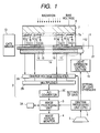
- FIG. 1 is a block diagram showing the configuration of
an image pickup apparatus according to a first embodiment of
the invention;
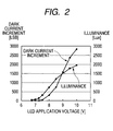
- FIG. 2 is a drawing showing the relationship between
application voltage of an LED of a light emission body of a
light application mechanism in the first embodiment of the
invention and illuminance change of the LED or dark current
component produced by light application of the LED;
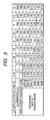
- FIG. 3 is a drawing showing the application voltages of
the LED and the decreasing rates of the dynamic range;
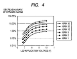
- FIG. 4 is a drawing showing the correspondence between
the application voltage of the LED and the decreasing rate of
the dynamic range for each representative gain setup value in
the electric signal processing circuit in the first embodiment
of the invention;
- FIG. 5 is a drawing showing response output waveforms
of electric signal processing circuit when strong radiation
is detected in the first embodiment of the image pickup apparatus
and comparative examples;
- FIG. 6 is a drawing showing response output waveforms
of electric signal processing circuit when weak radiation is
detected in the first embodiment of the image pickup apparatus
and comparative examples; and
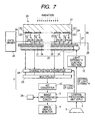
- FIG. 7 is a block diagram showing the configuration of
an image pickup apparatus according to a second embodiment of
the invention.
-
Detailed Description of the Invention
-
Referring now to the accompanying drawings, there are
shown preferred embodiments of radiological image pickup
apparatus of the invention (which is referred simply as image
pickup apparatus whenever necessary).
<First embodiment>
-
FIG. 1 is a block diagram showing the configuration of
an image pickup apparatus according to a first embodiment of
the invention and the internal structure of a flat-panel
radiation detector (radiation detector) of direct conversion
type, of the image pickup apparatus.
-
The radiological image pickup apparatus of the first
embodiment includes a flat-panel radiation detector of direct
conversion type (FPD) 1, an electric signal processing circuit
2, an image processing circuit 3, an image display monitor 4,
an operation section 5, and a central processing unit 6, as
shown in FIG. 1. The flat-panel radiation detector of direct
conversion type (FPD) 1 detects and takes out the spatial
distribution of incident radiation passing through the object
whose image is to be picked up (not shown) as an electric signal.
The electric signal processing circuit 2 amplifies the electric
signal taken out from the FPD 1. The image processing circuit
3 creates a radiological image of the obj ect based on the electric
signal amplified by the electric signal processing circuit 2.
The image display monitor 4 displays the radiological image
created by the image processing circuit 3. The operator
performs entry operation required for picking up an image the
through operation section 5. The central processing unit 6
performs necessary operations and control in response to entry
operation performed through the operation section 5 and the
advance state of the image pickup process. In the radiological
image pickup apparatus, the radiological image corresponding
to the radiological image passing through the object projected
onto the FPD 1 as radiation is applied to the object is displayed
on the image display monitor 4.
-
In the FPD 1, a common electrode 8 for applying a bias
voltage is formed on one side of a semiconductor layer 7 sensitive
to radiation and a two-dimensional array made up of a large
number of split electrodes 9 is formed on an opposite side.
A transparent glass substrate (TFT substrate) 12 is disposed
on the split electrode 9 formation side of the semiconductor
layer 7. The transparent glass substrate 12 is formed with
pairs of thin-film transistor switches (TFT switches) 10 and
capacitors 11, each pair for each spilt electrode 9, provided
in a one-to-one correspondence with pixels of a radiological
image.
-
That is, charges of the amount responsive to the radiation
incidence strength are accumulated in the capacitors 11 via
the split electrodes 9 as radiation is incident. A gate driver
13 switches on and off the TFT switches 10 in order according
to an external scan signal for reading the charges accumulated
in the capacitors 11, whereby an electric signal is taken out
and the spatial distribution of the incident radiation is
detected. In the embodiment, an intermediate layer 7a is placed
between the semiconductor layer 7 and the split electrodes 9.
-
The electric signal processing circuit 2 amplifies the
taken-out electric signal according to the gain value set by
the central processing unit 6 (gain setup value) and can also
increase or decrease the gain setup value. The gain setup value
usually is set so that it is decreased if the assumed incident
radiation strength increases and that it is increased if the
assumed incident radiation strength decreases (namely, so that
the incident radiation strength and the gain setup value are
in inverse proportion).
-
The electric signal processing circuit 2 is made up of
a charge (electric current)-voltage converter 2A, a multiplexer
2B, and an A/D converter 2C, and the gain setup value is set
in the charge-voltage converter 2A. In the embodiment, the
radiation strength of a radiation source (not shown) is also
controlled by the central processing unit 6, and the central
processing unit 6 sets the gain setup value of the electric
signal processing circuit 2 matching the radiation strength
of the radiation source.
-
The radiation strength may be detected separately and
the gain setup value matching the detected radiation strength
may be set automatically by the central processing unit 6.
-
The image processing circuit 3 has a correction
coefficient registration section 3A for registering an offset
correction coefficient and a sensitivity correction
coefficient. The offset correction coefficient is used for
correcting location variations in offset between electric
signals caused by location nonuniformity of the detection
channel of the FPD 1 for each electric signal to create a
radiological image. The sensitivity correction coefficient
is used for correcting location variations in sensitivity
between electric signals caused by location nonuniformity of
the detection channel of the FPD 1 for each electric signal
to create a radiological image. The image processing circuit
3 performs variation correction processing in the offset and
the sensitivity between the electric signals based on the
previously registered offset correction coefficient and
sensitivity correction coefficient.
-
The image pickup apparatus of the embodiment includes
a light application mechanism 14 and a light strength control
section 15. The light applicationmechanism (light application
section) 14 applies light to the entire surface of the split
electrode 9 formation side of the semiconductor layer 7 sensitive
to radiation. The light strength control section 15 controls
the light application mechanism 14 so as to increase or decrease
the strength of light applied by the light application mechanism
14 in response to a decrease or an increase in the gain setup
value of the electric signal processing circuit 2. The light
strength control section 15 controls the light application
mechanism 14 so that the strength of light applied by the light
application mechanism 14 increase if the gain setup value of
the electric signal processing circuit 2 decreases and that
the strength of light applied by the light application mechanism
14 decreases if the gain setup value increases (namely, so that
the gain setup value and the light strength are in inverse
proportion).
-
Therefore, in the embodiment, normally operation is
performed so that the incident radiation strength and the gain
setup value are in inverse proportion, and the gain setup value
and the light strength are in inverseproportion. Consequently,
the light strength control section 15 controls the light
application mechanism 14 so that the strength of light applied
by the light application mechanism 14 and the incident radiation
strength are in direct proportion.
-
In the embodiment, for example, proper applied light
strength is previously experimentally calculated about each
gain setup value and the applied light strength is registered
in association with each gain setup value. Then, at setting
the gain setup value, the corresponding applied light strength
is read and is set in the light strength control section 15.
-
Further, if the number of used radiation strengths is
previously limited to several, a proper gain setup value and
a proper applied light strength may be registered in association
with each other for each radiation strength. Then, if the
radiation strength is set, automatically the proper gain setup
value and the proper applied light strength may be set.
-
Specifically, the light application mechanism 14 may
include a light guide plate 16 made of a transparent acrylic
resin disposed so as to overlap the back of the TFT substrate
12 and a light emission body 17 such as a light emitting diode
or a cold-cathode tube placed on a side end face of the light
guide plate 16, as shown in FIG. 1. The surface of the light
guide plate 16 as the face overlapping the TFT substrate 12
may be micromachined (subj ected to surface roughness treatment)
and a reflection sheet 18 may be attached to the back of the
light guide plate 16. Further, a dispersion sheet 19 may be
placed between the TFT substrate 12 and the light guide plate
16.
-
In this case, light of the light emission body 17 passes
through the light guide plate 16 while it is reflected on the
reflection sheet 18, and is applied through the micromachined
surface of the light guide plate 16 and the dispersion sheet
19, so that the light can be applied efficiently and uniformly
to the split electrode 9 formation side of the semiconductor
layer 7.
-
As another specific configuration of the light
application mechanism 14, a surface light emitting diode may
be put on the TFT substrate 12 with a transparent adhesive with
its light emitting face directed for the TFT substrate 12. The
light strength control section 15 controls the light emission
amount of the light emission body 17 so that the light strength
of the light emission body 17 increases or decreases in response
to a decrease or an increase in the gain setup value, and also
controls so as to enable the light application mechanism 14
to apply light not only during detection of radiation, but also
before or after detection of radiation.
-
In the image pickup apparatus of the embodiment, as the
light application mechanism 14 applies light to the split
electrode 9 formation side of the semiconductor layer 7 and
the intermediate layer 7a sensitive to radiation in the FPD
1, space charges produced by the light application accumulate
in the space between the split electrodes 9 in the semiconductor
layer 7 and the intermediate layer 7a, and thus the charges
occurring as radiation is incident do not accumulate and are
taken out. Consequently, change in the effective sensitive
area does not occur and fluctuations in the detection sensitivity
of the FPD 1 can be circumvented.
-
If light application of the light application mechanism
14 is continued still after incidence of radiation stops, the
space charges accumulating in the space between the split
electrodes 9 are not taken out and continue to accumulate and
therefore occurrence of residual output can also be
circumvented.
-
Subsequently, the semiconductor layer 7 and the
intermediate layer 7a will be discussed more specifically.
-
Preferably, the wavelength of light applied to the
semiconductor layer 7 and the intermediate layer 7a is a
wavelength shorter than the transmittance half wavelength of
the semiconductor layer 7 and the intermediate layer 7a and
longer than the wavelength corresponding to band gap energy.
In this case, the wavelength of applied light is shorter than
the transmittance half wavelength of the used semiconductor
and is longer than the wavelength corresponding to band gap
energy. Thus, the applied light enters a part of the
semiconductor layer 7 deeply and a dead area widens. However,
the energy of the applied light is smaller than the gap band
energy, and thus damage to the semiconductor layer 7 (occurrence
of crystalline defect) caused by the applied light and an
increase in dark current caused by charge detection by the
applied light itself do not occur.
-
When amorphous semiconductor is used as the semiconductor
layer, this mode is particularly effective because damage action
to the semiconductor caused by the applied light is large in
amorphous semiconductor such as amorphous selenium (a-Se).
-
The wavelength at which the transmittance for the
intermediate layer 7a becomes 10% is about 710 nm, for example,
when amorphous selenium (a-Se) is used for the intermediate
layer 7a; it is about 660 nm when a thin film of antimonous
sulfide (Sb2S3) is used for the intermediate layer 7a.
-
Preferably, the semiconductor layer 7 is any of an
amorphous substance of undoped Se or an undoped Se compound,
an amorphous substance of Se doped with As or Te, or Se compound
doped with As or Te, an amorphous substance of Se doped with
alkali metal of Na, K, Li, etc., or an Se compound doped with
alkali metal of Na, K, Li, etc., an amorphous substance of Se
doped with halogen of F, Cl, etc., or an Se compound doped with
halogen of F, Cl, etc., or an amorphous substance of Se doped
with As, Te, alkali metal of Na, K, Li, etc., and halogen of
F, Cl, etc., in combination or Se compound.
-
Preferably, the semiconductor layer 7 is a
polycrystalline substance of any of compound semiconductors
CdTe, CdZnTe, PbI2, HgI2, TlBr, or GaAs or a polycrystalline
substance of the compound semiconductor doped with halogen of
F, Cl, etc.
-
Preferably, the wavelength of light applied to the
intermediate layer 7a is shorter than the transmittance half
wavelength of the intermediate layer 7a; further preferably
it is shorter than the wavelength at which the transmittance
for the intermediate layer 7a becomes 10%. If the intermediate
layer 7a has more defects than the semiconductor layer 7 and
charges accumulate in the intermediate layer 7a more easily
than the semiconductor layer 7, bend of an electric field occurs
only in the intermediate layer 7a. Therefore, in this case,
as light is applied to the intermediate layer 7a, fluctuations
in sensitivity and occurrence of residual output caused by the
effect of the charges accumulating in the space between the
split electrodes 9 are eliminated. As the wavelength of applied
light is made shorter than the transmittance half wavelength
of the intermediate layer 7a, most applied light is absorbed
in the intermediate layer 7a, so that the applied light reaching
the semiconductor layer 7 can be lessened. Therefore, dark
current of the semiconductor layer 7 caused by the applied light
can also be suppressed.
-
Preferably, the intermediate layer 7a is any of an
amorphous substance of undoped Se or an undoped Se compound,
an amorphous substance of Se doped with As or Te, or Se compound
doped with As or Te, an amorphous substance of Se doped with
alkali metal of Na, K, Li, etc., or an Se compound doped with
alkali metal of Na, K, Li, etc., an amorphous substance of Se
doped with halogen of F, Cl, etc., or an Se compound doped with
halogen of F, Cl, etc., or an amorphous substance of Se doped
with As, Te, alkali metal of Na, K, Li, etc., and halogen of
F, Cl, etc., in combination or Se compound.
-
However, to cause the intermediate layer 7a to function,
the material of the semiconductor layer 7 and that of the
intermediate layer 7a are made different.
-
Preferably, the intermediate layer 7a is a
polycrystalline substance of any of compound semiconductors
Sb2S3, CeO2, CdS, CdSe, CdTe, CdZnTe, ZnSe, ZnTe, ZnS, PbI2,
HgI2, TlBr, or GaAs or a polycrystalline substance of the compound
semiconductor doped with halogen of F, Cl, etc., or multilayer
using the polycrystalline substances in combination.
-
If the intermediate layer 7a has a transmission limit
wavelength between the transmittance half wavelength of the
semiconductor layer 7 and the wavelength corresponding to the
band gap energy, the filter effect can be provided for dealing
with the case where it is necessary to apply light to both the
semiconductor layer 7 and the intermediate layer 7a because
charges accumulate in both the semiconductor layer 7 and the
intermediate layer 7a. Specifically, as the material of the
semiconductor layer 7 and that of the intermediate layer 7a
are selected, the intermediate layer 7a is made to have the
transmission limit wavelength between the transmittance half
wavelength of the semiconductor layer 7 and the wavelength
corresponding to the band gap energy, whereby the filter effect
is produced for applying light to any desired depth. That is,
the short wavelength component of wavelength components of white
light is absorbed in the intermediate layer 7a and does not
deeply reach the semiconductor layer 7 and most light can be
made to act on the intermediate layer 7a without causing light
application damage of the semiconductor layer 7 or an increase
in dark current. The long wavelength component can be allowed
to pass through the intermediate layer 7a to reach the
semiconductor layer 7 and can be made to act thereon.
-
The intermediate layer 7a mentioned here is a layer having
carrier selectivity and has the effect of suppressing dark
current, etc. The carrier selectivity refers to the property
of remarkable difference between electrons and holes of charge
transfer carriers in a semiconductor in the contribution rate
to the charge transfer action.
-
For example, substances with large contribution of
electrons to the charge transfer action includes
polycrystalline substances such as CeO2, CdS, and CdSe of n-type
semiconductors and amorphous substances of amorphous Se, etc.,
doped with alkali metal or As or Te for lowering contribution
of holes. Substances with large contribution of holes to the
charge transfer action includes polycrystalline substances
such as ZnSe, ZnTe, and ZnS of p-type semiconductors and
amorphous substances of amorphous Se, etc., doped with halogen
for lowering contribution of electrons.
-
Further, there are also substances for providing large
contribution of electrons or large contribution of holes
depending on the film formation condition, such as Sb2S3, CdTe,
CdZnTe, PbI2, HgI2, TlBr, or undoped amorphous Se or Se compound.
-
To use a film of amorphous selenium (a-Se) 1 mm thick,
for example, as the semiconductor layer 7, the transmittance
half wavelength is 740 mm and the wavelength corresponding to
the band gap energy 2.2 eV is 560 nm. Therefore, a material
having a transmission limit wavelength in the range of 560 nm
to 740 nm may be used to form the intermediate layer 7a.
-
For example, the transmission limit wavelength of a thin
film of antimonous sulfide (Sb2S3) 1 µm thick is 580 nm and thus
if a thin film of antimonous sulfide 1 µm thick is formed as
the intermediate layer 7a between amorphous selenium and the
split electrodes 9, the short wavelength component of 580 nm
or less, of applied white light is cut and the energy of the
applied light becomes smaller than the band gap energy.
Therefore, damage to the semiconductor layer 7 caused by the
applied light and an increase in dark current are eliminated.
Although the material and thickness of the intermediate layer
7a need to be selected according to the material of the
semiconductor layer 7 to be used, the need for limiting the
wavelength of the applied light is eliminated and the
configuration involved in light application can be simplified.
In other words, even if a white light source is used rather
than a single-color light source as the applied light source,
a radiation detector with no fluctuations in sensitivity can
also be provided without causing light application damage or
an increase in dark current.
-
The intermediate layer 7a may be placed just below the
common electrode 8 rather than placed just above the split
electrodes 9 as described above and further if the intermediate
layer 7a is placed both just above the split electrodes 9 and
just below the common electrode 8, a similar advantage to that
of the configuration described above can also be provided. At
the time, the materials of the intermediate layers 7a need not
be the same.
-
Further, as the light strength control section 15 controls
the light application mechanism 14, the applied light strength
increases or decreases in response to a decrease or an increase
in the gain setup value of the electric signal processing circuit
2, as described above.
-
On the other hand, light application of the light
application mechanism 14 carries an increase in electric signal
with a dark current component added to the electric signal.
The dark current component accompanying light application of
the light application mechanism 14 increases or decreases in
response to an increase or a decrease in the applied light
strength; the dark current component increases as the applied
light strength increases.
-
As a result of also amplifying the dark current component
accompanying light application by the electric signal
processing circuit 2 in response to the gain setup value, the
dynamic range of the electric signal processing circuit 2 is
narrowed as much as the amplifieddark current component occupies
the output range of the electric signal processing circuit 2;
if the gain setup value increases, the amplification degree
of the dark current component increases and therefore for the
same amount of the dark current component, if the gain setup
value increases, the degree of narrowing the dynamic range also
increases.
-
In the embodiment, however, if the gain setup value of
the electric signal processing circuit 2 increases, the strength
of light applied by the light application mechanism 14 is
decreased and the dark current component decreases and thus
the increase in the gain setup value is offset by the decrease
in the dark current component and narrowing the dynamic range
with the increase in the gain setup value is suppressed. In
contrast, if the gain setup value of the electric signal
processing circuit 2 decreases, the strength of light applied
by the light application mechanism 14 is increased and the dark
current component increases. Then, the increase in the dark
current component is offset by the decrease in the gain setup
value and narrowing the dynamic range with the increase in the
applied light strength is suppressed.
-
Therefore, in the image pickup apparatus of the embodiment,
widely occupying the output range of the electric signal
processing circuit 2 by the dark current component occurring
with light application for circumventing fluctuations in the
detection sensitivity of the FPD 1 and occurrence of residual
output is eliminated and therefore a situation in which the
dynamic range is largely narrowed does not occur.
-
Subsequently, the process of finding the correspondence
between the gain setup value in the electric signal processing
circuit 2 and the applied light strength will be discussed
specifically.
-
FIG. 2 is a graph showing change in the illuminance (light
strength) of the light emitting diode (LED) of the light emission
body 17 of the light application mechanism 14 in response to
change in the application voltage of the LED and change in the
dark current component produced by light application of the
LED (dark current increment of the FPD 1). FIG. 2 assumes that
the gain setup value of the electric signal processing circuit
2 is 30 and the dynamic range is 8000 LSB. When the gain setup
value is changed, the dark current component produced by light
application of the LED becomes [GA/30] times if the gain setup
value is GA.
-
As shown in FIG. 2, often the illuminance of the LED does
not linearly change in response to change in the application
voltage of the LED, and the dark current component produced
by light application of the LED corresponding to the illuminance
of the LED does not correspond to the illuminance of the LED
at a constant rate. Therefore, the optimum application voltage
to the LED (illuminance of LED) is calculated in accordance
with how much the actual dark current component produced by
light application of the LED occupies the dynamic range
(decreasing rate of dynamic range).
-
FIG. 3 is a list of numeric data indicating the application
voltages of the LED and the decreasing rates of the dynamic
range corresponding thereto for each representative gain setup
value. FIG. 4 is a graph to indicate the correspondence between
the application voltage of the LED and the decreasing rate of
the dynamic range for each representative gain setup value.
-
The decreasing rate of the dynamic range as a guideline
varies depending on the type of radiological image of object
to be picked up, etc.; for a medical radiological image requiring
a wide dynamic range, it is desirable that the decreasing rate
of the dynamic range should be 1% or less. Therefore, if the
optimum application voltages of the LED for stepwise gain setup
values in the electric
signal processing circuit 2 are calculated,
they are as listed in Table 1.
| Gain | 1 | 2 | 5 | 10 | 20 | 30 |
| Optimum LED voltage [V] | 10 | 8.5 | 7.7 | 7.3 | 7.2 | 7.0 |
-
In the embodiment, the specific control systems of the
light strength of the
light emission body 17 of the
light
application mechanism 14 are as follows:
- (Control system A) The optimum correspondences between
the stepwise gain setup values and the application voltages
of the LED are previously registered. To set the gain setup
value in response to a stepwise increase or decrease in the
gain setup value, the corresponding application voltage of the
LED is read and is set in the light strength control section
15 and the LED of the light emission body 17 is lighted according
to the setup application voltage. In this case, open loop
control is applied.
- (Control system B) The gain setup value is changed to
a new one in response to a stepwise increase or decrease in
the gain setup value, light of the light emission body 17 is
turned on and off, and each dark current value is measured.
What percentage of the dynamic range the difference between
the dark current values becomes is calculated and further whether
or not the calculation value is equal to or less than a
predetermined decreasing rate of the dynamic range (for example,
1%) is checked. The process is repeated until the calculation
value becomes equal to or less than the predetermined decreasing
rate of the dynamic range (for example, 1%) while the light
strength of the light emission body 17 is increased or decreased.
In this case, feedback control is applied.
- (Control system C) The continuous optimum
correspondences between the gain setup values and the
application voltages of the LED are calculated in the form of
mathematical expression and are previously registered. To set
the gain setup value in response to a stepwise increase or
decrease in the gain setup value, the corresponding application
voltage of the LED is fetched using the mathematical expression
and is set in the light strength control section 15 and the
LED of the light emission body 17 is lighted according to the
setup application voltage. In this case, open loop control
is applied.
- (Control system D) The continuous optimum
correspondences between the gain setup values and the
application voltages of the LED are calculated in the table
format as shown below and are previously registered. To set
the gain setup value in response to a continuous increase or
decrease in the gain setup value, the corresponding application
voltage of the LED is referenced and fetched from the table
and is set in the light strength control section 15 and the
LED of the light emission body 17 is lighted according to the
setup application voltage. Also in this case, open loop control
is applied.
[Example of continuous optimum correspondences between gain
setup values and application voltages of LED]
| Gain setup value 1.0 | LED application voltage 10.0 V |
| Gain setup value 1.1 | LED application voltage 9.7 V |
| Gain setup value 1.2 | LED application voltage 9.5 V |
| Gain setup value 1.3 | LED application voltage 9.3 V |
- (Control system E) The gain setup value is changed to a new
one in response to a continuous increase or decrease in the
gain setup value, light of the light emission body 17 is turned
on and off, and each dark current value is measured. What
percentage of the dynamic range the difference between the dark
current values becomes is calculated and further whether or
not the calculation value is equal to or less than a predetermined
decreasing rate of the dynamic range (for example, 1%) is checked.
The process is repeated until the calculation value becomes
equal to or less than the predetermined decreasing rate of the
dynamic range (for example, 1%) while the light strength of
the light emission body 17 is increased or decreased. In this
case, feedback control is applied.
-
-
In the image pickup apparatus of the embodiment, the split
electrodes 9 are transparent or semitransparent at the
wavelength of the light applied by the light application
mechanism 14. If the split electrodes 9 are thus transparent
or semitransparent, the applied light is applied not only to
the space between the split electrodes 9, but also to the split
electrode 9 formation area. Thus, if radiation at a higher
rate than the taking-out speed of charges is incident and charges
once accumulate in the proximity of the split electrodes 9,
they are instantly again excited by the energy of the applied
light and Kinetic energy is given, so that the potential profile
is not distorted and the potential in the proximity of the split
electrodes 9 does not rise. Therefore, for example, to use
a-Se which needs to be used with a high bias applied, the normal
operation of the TFT switches 10 can also be maintained.
-
In the image pickup apparatus of the embodiment, to perform
variation correction processing in the offset and sensitivity
between electric signals by the image processing circuit 3 based
on the previously registered offset correction coefficient and
sensitivity correction coefficient, the strength of the light
applied by the light application mechanism 14 is reflected.
-
That is, the offset correction coefficient and the
sensitivity correction coefficient are previously calculated
by the image processing circuit 3 or the central processing
unit 6 using a phantom (standard object) for registering the
correction coefficients and are registered in the correction
coefficient registration section 3A. In this case, the
strength of the light appliedby the light application mechanism
14 is previously assumed to be in several steps and the offset
correction coefficient and the sensitivity correction
coefficient are calculated in each assumed step of the light
strength and are registered in the correction coefficient
registration section 3A. The offset correction coefficient
and the sensitivity correction coefficient corresponding to
the strength of the light applied in actual picking up an image
are read and variation correction processing is performed.
-
Therefore, the image processing circuit 3 performs offset
and sensitivity variation correction processing so that the
strength of the light appliedbythe light application mechanism
14 is reflected based on the offset correction coefficient and
the sensitivity correction coefficient already registered in
the correction coefficient registration section 3A.
Consequently, an error can be prevented from occurring in the
offset and sensitivity variation corrections as light is applied
by the light application mechanism 14.
-
Next, the forming method of the image pickup apparatus
of the first embodiment is as follows:
-
For the FPD 1 of the image pickup apparatus of the
embodiment, transparent electrodes of ITO films, etc., are
formed on the TFT substrate 12 as the split electrodes 9 and
then a thin film of antimonous sulfide (Sb2S3) 1 µm thick is
first formed as the intermediate layer 7a and next a thick film
of amorphous selenium (a-Se) semiconductor 1 mm thick is formed
as the semiconductor layer 7 sensitive to radiation. Then,
a thin film of gold (Au) 0.1 µm thick is formed on the thick
film of amorphous selenium (a-Se) semiconductor as the common
electrode 8. A surface light emitting diode of green light
emitting type is put on the back of the TFT substrate 12 with
a transparent adhesive, whereby the light application mechanism
14 is disposed.
-
Next, the radiation detection operation of the image
pickup apparatus of the embodiment is as follows:
-
As radiation, X-rays applied under the condition of tube
voltage 55 kV and tube current 80 mA from an X-ray tube with
an AL filter placed at a distance of 1 m from the FPD 1 were
used. To apply strong X-rays, an AL filter 1 mm thick was used;
to apply weak X-rays, an AL filter 26 mm thick was used. The
digital output of the electric signal processing circuit 2 was
set to the full range of 8000 [LSB].
-
The response output waveforms of the electric signal
processing circuit 2 when X-rays were applied for four seconds
and then stopped in operation conditions (1) to (5) listedbelow
were measured, and the decreasing rate of the dynamic range
caused by the dark current increment produced by light
application, the degree of fluctuations in the detection
sensitivity, and the degree of occurrence of residual output
were calculated from the measurement data.
-
FIGS. 5 and 6 show the measurement results of the response
output waveforms of the electric signal processing circuit 2,
and Table 2 lists the results of the decreasing rate of the
dynamic range, the degree of fluctuations in the detection
sensitivity, the degree of occurrence of residual output, and
the like.
Operation condition (1)
-
- Application of strong X-rays
- Gain setup value of charge-voltage converter 2A: 1
- Supply voltage from light strength control section 15
to surface light emitting diode: 10 V
-
Operation condition (2)
-
- Application of weak X-rays
- Gain setup value of charge-voltage converter 2A: 30
- Supply voltage from light strength control section 15
to surface light emitting diode: 7 V
-
Operation condition (3)
-
- Application of strong X-rays
- Gain setup value of charge-voltage converter 2A: 1
- Supply voltage from light strength control section 15
to surface light emitting diode: 7 V
-
Operation condition (4)
-
- Application of weak X-rays
- Gain setup value of charge-voltage converter 2A: 30
- Supply voltage from light strength control section 15
to surface light emitting diode: 10 V
-
Operation condition (5)
-
- Application of strong X-rays
- Gain setup value of charge-voltage converter 2A: 1
- Supply voltage from light strength control section 15
to surface light emitting diode: None
-
-
The operation conditions (1) and (2) are applied to the
first embodiment, and the operation conditions (3) to (5) are
applied to comparative examples.
| | Fluctuations in detection sensitivity | Occurrence of residual output | Dark current increment | Decreasing rate of dynamic range |
| Operation condition (1) | Small | Small | 65 LSB | 0.81% |
| Operation condition (2) | Small | Small | | 60 LSB | 0.75% |
| Operation condition (3) | Medium | Medium | | 2 LSB | 0.03% |
| Operation condition (4) | Small | Small | 1950 LSB | 24% |
| Operation condition (5) | Large | Large | None | | 0% |
-
Making a comparison between the embodiment and the
comparative examples with respect to the data of fluctuations
in detection sensitivity and occurrence of residual output in
Table 2 and the response output waveforms in FIGS. 5 and 6,
it is seen that when light is applied by the light application
mechanism 14, controlling the light strength is effective for
circumventing fluctuations in detection sensitivity and
occurrence of residual output. Particularly, making a
comparison between the response output waveforms in the
embodiment and the comparative example in FIG. 6, it is seen
that when light is applied by the light application mechanism
14, controlling is performed so that the applied light strength
increases or decreases in response to a decrease or an increase
in the gain setup value of the electric signal processing circuit
2, whereby a drastic decrease in the dynamic range can be
circumvented.
<Second embodiment>
-
FIG. 7 is a block diagram showing the configuration of
an image pickup apparatus according to a second embodiment of
the invention and the internal structure of a flat-panel
radiation detector (radiation detector) of indirect conversion
type, of the image pickup apparatus.
-
The image pickup apparatus of the second embodiment has
the same configuration and advantages as the image pickup
apparatus of the first embodiment except that it detects
radiation using a flat-panel radiation detector (radiation
detector) of indirect conversion type and therefore parts
identical with or similar to those previously described with
reference to FIG. 1 are denoted by the same reference numerals
in FIG. 7 and will not be discussed again.
-
The radiological image pickup apparatus of the second
embodiment includes a flat-panel radiation detector of indirect
conversion type (FPD) 20, an electric signal processing circuit
2, an image processing circuit 3, an image display monitor 4,
an operation section 5, and a central processing unit 6, as
shown in FIG. 7. The flat-panel radiation detector of indirect
conversion type (FPD) 20 detects and takes out the spatial
distribution of incident radiation passing through the object
whose image is to be picked up (not shown) in the form of an
electric signal. The electric signal processing circuit 2
amplifies the electric signal taken out from the FPD 20. The
image processing circuit 3 creates a radiological image of the
object based on the electric signal amplified by the electric
signal processing circuit 2. The image display monitor 4
displays the radiological image created by the image processing
circuit 3. The operator performs entry operation required for
picking up an image through the operation section 5. The central
processing unit 6 performs necessary operations and control
in response to entry operation performed through the operation
section 5 and the advance state of the image pickup process.
Therefore, the radiological image corresponding to the
radiological image passing through the object projected onto
the FPD 20 as radiation is applied to the object is displayed
on the image display monitor 4.
-
In the FPD 20, a two-dimensional array made up of a large
number of semiconductor optical sensors 24 is formed on one
side of a radiation-light conversion layer 21 for converting
radiation into light. The semiconductor optical sensors 24
are provided by electrically splitting a semiconductor layer
22 sensitive to light, each having an electric signal output
electrode 23 on the back of the semiconductor layer 22. A
transparent glass substrate (TFT substrate) 27 is disposed on
the semiconductor optical sensor 24 formation side of the
radiation-light conversion layer 21. The transparent glass
substrate (TFT substrate) 27 is formed with pairs of thin-film
transistor switches (TFT) 25 and capacitors 26, each pair for
each semiconductor optical sensor 24, provided in a one-to-one
correspondence with pixels of a radiological image.
-
That is, charges of the amount responsive to the radiation
incidence strength are accumulated in the capacitors 26 via
the semiconductor optical sensors 24 as radiation is incident.
Then, a gate driver 28 switches on and off the TFT switches
25 in order according to an external scan signal for reading
the charges accumulated in the capacitors 26, whereby light
occurring in the radiation-light conversion layer 21 by the
incident radiation is taken out as an electric signal from each
of the semiconductor optical sensors 24 and the spatial
distribution of the incident radiation is detected.
-
The image pickup apparatus of the second embodiment also
includes a light application mechanism (light application
section) 29 and a light strength control section 30. The light
application mechanism 29 applies light to the entire surface
of the semiconductor optical sensor 24 formation side of the
radiation-light conversion layer 21. The light strength
control section 30 controls the light application mechanism
29 so as to increase or decrease the strength of light applied
by the light application mechanism 29 in response to a decrease
or an increase in the gain setup value of the electric signal
processing circuit 2.
-
The light strength control section 30 controls the light
application mechanism 29 so that the strength of light applied
by the light application mechanism 29 increases if the gain
setup value of the electric signal processing circuit 2 decreases
and that the strength of light applied by the light application
mechanism 29 decreases if the gain setup value increases (namely,
so that the gain setup value and the light strength are in inverse
proportion).
-
Therefore, also in the embodiment, normally operation
is performed so that the incident radiation strength and the
gain setup value are in inverse proportion, and the gain setup
value and the light strength are in inverse proportion.
Consequently, the light strength control section 30 controls
the light application mechanism 29 so that the strength of light
applied by the light application mechanism 29 and the incident
radiation strength are in direct proportion.
-
Also in the embodiment, for example, proper applied light
strength is previously experimentally calculated about each
gain setup value and the applied light strength is registered
in association with each gain setup value and to set the gain
setup value, the corresponding applied light strength is read
and is set in the light strength control section 30.
-
Further, if the number of used radiation strengths is
previously limited to several, a proper gain setup value and
a proper applied light strengthmaybe registered in association
with each other for each radiation strength and if the radiation
strength is set, automatically the proper gain setup value and
the proper applied light strength may be set.
-
In the FPD 20, the electric signal output electrode 23
of each the semiconductor optical sensor 24 on the side thereof
on which light from the light application mechanism 29 is
incident is formed of an opaque material such as Al or Ta and
has a light shield function for shielding the light from the
light application mechanism 29 so that the light is not directly
detected by the semiconductor optical sensor 24. The light
from the light application mechanism 29 is not radiation to
be detected and thus is not directly detected by the
semiconductor optical sensor 24.
-
Specifically, the light application mechanism 29 may
include a light guide plate 31 made of a transparent acrylic
resin disposed so as to overlap the back of the TFT substrate
27 and a light emission body 32 such as a light emitting diode
or a cold-cathode tube placed on a side end face of the light
guide plate 31, as shown in FIG. 7. The surface of the light
guide plate 31 as the face overlapping the TFT substrate 27
may be micromachined (subjected to surface roughness treatment)
and a reflection sheet 33 may be attached to the back of the
light guide plate 31. A dispersion sheet 34 maybe placed between
the TFT substrate 27 and the light guide plate 31.
-
In this case, light of the light emission body 32 passes
through the light guide plate 31 while it is reflected on the
reflection sheet 33, and is applied through the micromachined
surface of the light guide plate 31 and the dispersion sheet
34, so that the light can be applied efficiently and uniformly
to the semiconductor optical sensor 24 formation side of the
radiation-light conversion layer 21.
-
As another specific configuration of the light
application mechanism 29, a surface light emitting diode may
be put on the TFT substrate 27 with a transparent adhesive with
its light emitting face directed for the TFT substrate 27. The
light strength control section 30 controls the light emission
amount of the light emission body 32 so that the light strength
of the light emission body 32 increases or decreases in response
to a decrease or an increase in the gain setup value, and also
controls so as to enable the light application mechanism 29
to apply light not only during detection of radiation, but also
before or after detection of radiation.
-
In the image pickup apparatus of the embodiment, as the
light application mechanism 29 applies light to the
semiconductor optical sensor 24 formation side of the
radiation-light conversion layer 21 for converting radiation
into light in the FPD 20, space charges produced by the light
application accumulate in the space between the semiconductor
optical sensors 24 and thus the charges occurring as radiation
is incident do not accumulate and are taken out. Consequently,
change in the effective sensitive area does not occur and
fluctuations in the detection sensitivity of the FPD 20 can
be circumvented.
-
If light application of the light application mechanism
29 is continued still after incidence of radiation stops, the
space charges accumulating in the space between the
semiconductor optical sensors 24 are not taken out and continue
to accumulate and therefore occurrence of residual output can
also be circumvented.
-
Further, as the light strength control section 30 controls
the light application mechanism 29, the applied light strength
increases or decreases in response to a decrease or an increase
in the gain setup value of the electric signal processing circuit
2, as described above.
-
On the other hand, light application of the light
application mechanism 29 carries an increase in electric signal
with a dark current component added to the electric signal.
The dark current component accompanying light application of
the light application mechanism 29 increases or decreases in
response to an increase or a decrease in the applied light
strength; the dark current component increases as the applied
light strength increases.
-
As a result of also amplifying the dark current component
accompanying light application by the electric signal
processing circuit 2 in response to the gain setup value, the
dynamic range of the electric signal processing circuit 2 is
narrowed as much as the amplified dark current component occupies
the output range of the electric signal processing circuit 2;
if the gain setup value increases, the amplification degree
of the dark current component increases and therefore for the
same amount of the dark current component, if the gain setup
value increases, the degree of narrowing the dynamic range also
increases.
-
In the embodiment, however, if the gain setup value of
the electric signal processing circuit 2 increases, the strength
of light applied by the light application mechanism 29 is
decreased and the dark current component decreases and thus
the increase in the gain setup value is offset by the decrease
in the dark current component and narrowing the dynamic range
with the increase in the gain setup value is suppressed. In
contrast, if the gain setup value of the electric signal
processing circuit 2 decreases, the strength of light applied
by the light application mechanism 29 is increased and the dark
current component increases. Then, the increase in the dark
current component is offset by the decrease in the gain setup
value and narrowing the dynamic range with the increase in the
applied light strength is suppressed.
-
Therefore, in the image pickup apparatus of the embodiment,
widely occupying the output range of the electric signal
processing circuit 2 by the dark current component occurring
with light application for circumventing fluctuations in the
detection sensitivity of the FPD 20 and occurrence of residual
output is eliminated and therefore a situation in which the
dynamic range is largely narrowed does not occur.
-
The invention is not limited to the embodiments described
above and the following modifications can be made:
- (1) In the second embodiment, the light shield function
of each electric signal output electrode 23 in the FPD 20 prevents
the semiconductor optical sensor 24 from directly detecting
the light of the light application mechanism 29. However, the
electric signal output electrodes 23 may be optically
transparent electrodes and an opaque pattern having a light
shield function may be placed for each semiconductor optical
sensor 24 on the surface of the light guide plate 31, for example,
on the side of the light application mechanism 29 so as to prevent
the semiconductor optical sensors 24 from detecting the light
of the light application mechanism 29 in the presence of the
opaque pattern.
- (2) A laser diode (LD) or an electroluminescent (EL) device
can also be used as the light emission body of the light
application mechanism in the embodiments.
- (3) The image pickup apparatus of the invention can be
applied not only to a medical apparatus, such as an X-ray
fluoroscopic and radiographic apparatus, but also to an
industrial apparatus, such as an X-ray non-destructive
inspection apparatus, and the like.
-
-
As seen from the description made above, according to
the first aspect of the radiological image pickup apparatus,
the light application section applies light to the split
electrode formation side of the semiconductor layer sensitive
to radiation in the radiation detector and space charges produced
by the light application accumulate in the space between the
split electrodes and thus the charges occurring as radiation
is incident do not accumulate and are taken out. Consequently,
change in the effective sensitive area does not occur and
fluctuations in the detection sensitivity of the radiation
detector canbe circumvented. If light application is continued
still after incidence of radiation stops, the space charges
accumulating in the space between the split electrodes are not
taken out and continue to accumulate and therefore occurrence
of residual output can also be circumvented.
-
If the gain setup value of the electric signal processing
circuit increases, the strength of light applied by the light
application section is decreased and the dark current component
decreases and thus the increase in the gain setup value is offset
by the decrease in the dark current component and narrowing
the dynamic range with the increase in the gain setup value
is suppressed. In addition, in contrast, if the gain setup
value of the electric signal processing circuit decreases, the
strength of light applied by the light application section is
increased and the dark current component increases. Then, the
increase in the dark current component is offset by the decrease
in the gain setup value, narrowing the dynamic range with the
increase in the applied light strength is also suppressed, and
the dark current component narrowing the dynamic range does
not widely occupy the output range of the electric signal
processing circuit. Consequently, a situation in which the
dynamic range is largely narrowed does not occur.
-
Further, according to the fourth aspect of the
radiological image pickup apparatus, the light application
section applies light to the semiconductor optical sensor
formation side of the radiation-light conversion layer in the
radiation detector so that the light is not directly detected
by the semiconductor optical sensors, and the light of the light
application section is not directly detected by the
semiconductor optical sensors, so that the detection operation
of the semiconductor optical sensors is not hindered. Space
charges produced by the light application accumulate in the
space between the semiconductor optical sensors and thus the
charges occurring as radiation is incident do not accumulate
and are taken out. Consequently, change in the effective
sensitive area does not occur and fluctuations in the detection
sensitivity of the radiation detector can be circumvented.
-
If light application is continued still after incidence
of radiation stops, the space charges accumulating in the space
between the semiconductor optical sensors are not taken out
and continue to accumulate and therefore occurrence of residual
output can also be circumvented.
-
If the gain setup value of the electric signal processing
circuit increases, the strength of light applied by the light
application section is decreased and the dark current component
decreases and thus the increase in the gain setup value is offset
by the decrease in the dark current component and narrowing
the dynamic range with the increase in the gain setup value
is suppressed. In addition, in contrast, if the gain setup
value of the electric signal processing circuit decreases, the
strength of light applied by the light application section is
increased and the dark current component increases. Then, the
increase in the dark current component is offset by the decrease
in the gain setup value, narrowing the dynamic range with the
increase in the applied light strength is also suppressed, and
the dark current component narrowing the dynamic range does
not widely occupy the output range of the electric signal
processing circuit. Consequently, a situation in which the
dynamic range is largely narrowed does not occur.