EP1465261A1 - Method for absorbing electromagnetic wave using solar cell - Google Patents
Method for absorbing electromagnetic wave using solar cell Download PDFInfo
- Publication number
- EP1465261A1 EP1465261A1 EP20020724678 EP02724678A EP1465261A1 EP 1465261 A1 EP1465261 A1 EP 1465261A1 EP 20020724678 EP20020724678 EP 20020724678 EP 02724678 A EP02724678 A EP 02724678A EP 1465261 A1 EP1465261 A1 EP 1465261A1
- Authority
- EP
- European Patent Office
- Prior art keywords
- solar cell
- cells
- reflected
- electromagnetic
- wave
- Prior art date
- Legal status (The legal status is an assumption and is not a legal conclusion. Google has not performed a legal analysis and makes no representation as to the accuracy of the status listed.)
- Withdrawn
Links
Images


Classifications
-
- H—ELECTRICITY
- H10—SEMICONDUCTOR DEVICES; ELECTRIC SOLID-STATE DEVICES NOT OTHERWISE PROVIDED FOR
- H10F—INORGANIC SEMICONDUCTOR DEVICES SENSITIVE TO INFRARED RADIATION, LIGHT, ELECTROMAGNETIC RADIATION OF SHORTER WAVELENGTH OR CORPUSCULAR RADIATION
- H10F19/00—Integrated devices, or assemblies of multiple devices, comprising at least one photovoltaic cell covered by group H10F10/00, e.g. photovoltaic modules
- H10F19/90—Structures for connecting between photovoltaic cells, e.g. interconnections or insulating spacers
- H10F19/902—Structures for connecting between photovoltaic cells, e.g. interconnections or insulating spacers for series or parallel connection of photovoltaic cells
-
- H—ELECTRICITY
- H10—SEMICONDUCTOR DEVICES; ELECTRIC SOLID-STATE DEVICES NOT OTHERWISE PROVIDED FOR
- H10F—INORGANIC SEMICONDUCTOR DEVICES SENSITIVE TO INFRARED RADIATION, LIGHT, ELECTROMAGNETIC RADIATION OF SHORTER WAVELENGTH OR CORPUSCULAR RADIATION
- H10F19/00—Integrated devices, or assemblies of multiple devices, comprising at least one photovoltaic cell covered by group H10F10/00, e.g. photovoltaic modules
- H10F19/80—Encapsulations or containers for integrated devices, or assemblies of multiple devices, having photovoltaic cells
-
- H—ELECTRICITY
- H10—SEMICONDUCTOR DEVICES; ELECTRIC SOLID-STATE DEVICES NOT OTHERWISE PROVIDED FOR
- H10F—INORGANIC SEMICONDUCTOR DEVICES SENSITIVE TO INFRARED RADIATION, LIGHT, ELECTROMAGNETIC RADIATION OF SHORTER WAVELENGTH OR CORPUSCULAR RADIATION
- H10F77/00—Constructional details of devices covered by this subclass
-
- H—ELECTRICITY
- H10—SEMICONDUCTOR DEVICES; ELECTRIC SOLID-STATE DEVICES NOT OTHERWISE PROVIDED FOR
- H10F—INORGANIC SEMICONDUCTOR DEVICES SENSITIVE TO INFRARED RADIATION, LIGHT, ELECTROMAGNETIC RADIATION OF SHORTER WAVELENGTH OR CORPUSCULAR RADIATION
- H10F77/00—Constructional details of devices covered by this subclass
- H10F77/40—Optical elements or arrangements
- H10F77/42—Optical elements or arrangements directly associated or integrated with photovoltaic cells, e.g. light-reflecting means or light-concentrating means
- H10F77/48—Back surface reflectors [BSR]
-
- H—ELECTRICITY
- H10—SEMICONDUCTOR DEVICES; ELECTRIC SOLID-STATE DEVICES NOT OTHERWISE PROVIDED FOR
- H10W—GENERIC PACKAGES, INTERCONNECTIONS, CONNECTORS OR OTHER CONSTRUCTIONAL DETAILS OF DEVICES COVERED BY CLASS H10
- H10W90/00—Package configurations
- H10W90/701—Package configurations characterised by the relative positions of pads or connectors relative to package parts
- H10W90/751—Package configurations characterised by the relative positions of pads or connectors relative to package parts of bond wires
- H10W90/753—Package configurations characterised by the relative positions of pads or connectors relative to package parts of bond wires between laterally-adjacent chips
-
- Y—GENERAL TAGGING OF NEW TECHNOLOGICAL DEVELOPMENTS; GENERAL TAGGING OF CROSS-SECTIONAL TECHNOLOGIES SPANNING OVER SEVERAL SECTIONS OF THE IPC; TECHNICAL SUBJECTS COVERED BY FORMER USPC CROSS-REFERENCE ART COLLECTIONS [XRACs] AND DIGESTS
- Y02—TECHNOLOGIES OR APPLICATIONS FOR MITIGATION OR ADAPTATION AGAINST CLIMATE CHANGE
- Y02E—REDUCTION OF GREENHOUSE GAS [GHG] EMISSIONS, RELATED TO ENERGY GENERATION, TRANSMISSION OR DISTRIBUTION
- Y02E10/00—Energy generation through renewable energy sources
- Y02E10/50—Photovoltaic [PV] energy
- Y02E10/52—PV systems with concentrators
Definitions
- the present invention relates to electromagnetic-wave absorbing methods using a solar cell or cells and in particular to methods of absorbing electromagnetic waves with a solar cell or cells whereby there comes about essentially no reflection of electromagnetic waves without impeding solar light power generation by the solar cell or cells.
- a measure can be taken in the reception side but basically it is important that the wall surfaces of such a high building be adapted not to reflect electromagnetic waves. Especially these days that the city is flooded with electromagnetic waves from cellular phones or the like, an unforeseen accident can be predicted and a technique of preventing electromagnetic waves from being reflected is being sought.
- the use of a ferrite-type electromagnetic-wave absorbing wall having a ferrite tile embedded in a curtain wall has so far been proposed for a building wall surface.
- the ferrite-type electromagnetic-wave absorbing wall inapplicable to absorbing electromagnetic waves in the UHF band, but also it is heavy in weight, and rather hard to construct practically and economically.
- the ferrite-type electromagnetic-wave absorber wall has scarcely come into wide use in general buildings.
- the present invention has for its object to provide an electromagnetic wave absorbing method using a solar cell or cells, which can prevent the reflection of electromagnetic waves without impeding solar light power generation by the solar cell or cells.
- a method of absorbing electromagnetic waves with a solar cell or cells characterized by adjusting impedance of a solar cell to electromagnetic waves incident thereon so that there is virtually no reflection of the electromagnetic wave by the solar cell.
- the impedance can be adjusted specifically by changing or adjusting the way in which the solar cells are wired together.
- the impedance can also be adjusted specifically by appending a capacitor across output terminals of a solar cell module.
- the impedance can also be adjusted specifically by appending an electronic component or components to the solar cell or cells internally or externally thereof.
- the impedance of the solar cell or cells is matched to an electromagnetic-wave characteristic impedance; hence there comes about virtually no reflection of an electric wave by the solar cell or solar cells.
- a protective film and semiconductor layers making up a solar cell act as dielectrics for electromagnetic waves in the UHF and VHF ranges while a wiring conductor being metallic in the solar cell acts as a reflector.
- Changing the distribution of wiring conductors in solar cells changes the boundary condition for electromagnetic waves and changes the capacitance and inductance; hence that can be used to adjust the impedance of a solar cell to electromagnetic waves incident thereon.
- the solar cells making up the module can be adjusted in their arrangement and then wired together.
- the impedance can also be adjusted by appending a capacitor across a pair of output terminals of the solar cell module, or by appending an electronic component such as a capacitor to a solar cell internally or externally thereof.
- a method of absorbing electromagnetic waves with a solar cell or cells characterized by arranging a plurality of solar cell modules different in shape and/or surface area in such a manner that reflected waves from the individual solar cell modules vary in phase so that they are canceled one by another.
- the modules can be so arranged that the reflected waves may be formed which are opposite in phase to one another and can thus be cancelled one by another.
- a plurality of solar cells can be connected together in the form of an antenna such as to absorb electromagnetic waves.
- a plurality of solar cells may be connected together in the form of a loop and a matching load may then be connected across loop ends of the loop.
- upper and lower electrodes of a plurality of solar cells may be connected respectively in series, and a matching load may then be connected across a pair of output terminals leading from such an upper and a lower electrode.
- the solar cells are allowed to act as a loop antenna or a patch antenna and the matching load to act to absorb the electromagnetic energy; hence virtually no reflected wave is produced.
- the present invention also provides a method of absorbing electromagnetic waves with a solar cell or cells, characterized by adjusting respective thicknesses of various layers of a solar cell so that reflected waves reflected, respectively, by these layers interfere with one another and are thereby cancelled one by another.
- the present invention also provides a method of absorbing electromagnetic waves with a solar cell or cells, characterized by forming an solar cell with an electromagnetic-wave reflector on a rear surface thereof and with a reticular electromagnetic-wave reflector on a top surface thereof in an arrangement such that a reflected wave being reflected by the electromagnetic-wave reflector on the rear surface and a reflected wave being reflected by the reticular electromagnetic-wave reflector may interfere with each other and be thereby cancelled each by other.
- the present invention also provides a method of absorbing electromagnetic waves with a solar cell, characterized by forming an electromagnetic-wave reflector on a wall surface over which a solar cell is to be mounted and forming a reticular electromagnetic-wave reflector on a top surface of the solar cell, in an arrangement such that a reflected wave being reflected by the electromagnetic-wave reflector on the wall surface and a reflected wave being reflected by the reticular electromagnetic-wave reflector may interfere with each other and be thereby cancelled each by other.
- FIG. 1 is a typical cross sectional view illustrating a first form of implementation of the present invention.
- a solar cell module 10 according to the present invention is made up of a plurality of solar cells 1 connected one to another by conductors 7 wherein each solar cell 1 comprises an upper electrode 2, a transparent electrode 3, a semiconductor p-layer 4, a semiconductor n-layer 5 and a lower electrode 6.
- the solar cells 1 are connected parallel to each other with the upper electrodes 2 in the adjacent cells 1 connected together and the lower electrode 6 used in common, and further with a capacitor 13 connected across output terminals 8 and 9 of the solar cell module, although the capacitor 13 may be omitted and the solar cells 1 may be connected in series or connected both in series and parallel in any of various possible combinations.
- the impedance Z of the solar cells 1 seen from the electromagnetic waves 12 incident thereon can be adjusted by so changing or adjusting.
- the impedance Z can be adjusted, e. g., by changing or adjusting the number of series- and/or parallel-connected solar cells.
- the impedance can be adjusted by changing or adjusting the way in which a module or modules made of series-connected cells and a module or modules made of parallel-connected cells are combined together.
- the impedance Z can be adjusted more finely by changing or adjusting the way in which they are so combined when series-connected cells and parallel-connected cells are different in number.
- the impedance Z can be adjusted by connecting a capacitor 13 across output terminals 8 and 9 of the module.
- an electronic component as a capacitor may be attached to each of all or selected ones of the solar cells 1 externally or internally thereof. The capacitor passes no direct current and hence exerts no influence on solar light power generation. If in any of these ways the impedance Z of the solar cell or cells is so adjusted that the same becomes equal to electromagnetic-wave characteristic impedance Z 0 , then the reflection coefficient ⁇ becomes zero and virtually no reflection of the electromagnetic wave comes about.
- Fig. 2 is a diagram illustrating a second form of implementation of the present invention.
- reference numerals 21 and 22 indicate solar cell modules different in surface area, which are shown as arranged lying on a wall surface.
- the impedances Z a , Z b , Z aa , and Z bb can be adjusted by changing or adjusting the areas of solar cell modules, the manner in which they are wired, and the way in which they are arranged, or upon additionally connecting an electronic component such as a capacitor to the modules internally or externally thereof.
- Fig. 3 is a diagram of the vector representation of phase angles of reflected waves from a plurality of modules which differ in phase angle in reflection coefficient. As shown, if a variety of phase angles 31 exist, then there come to be made pairs of reflected waves which cancel each other and, as a result, virtually any reflected wave is no longer emitted.
- Fig. 4 shows diagrams illustrating a third form of implementation of the present invention.
- a plurality of solar cells 1 arranged in the form of a loop with their upper or lower electrodes connected in series and with a matching load 41 such as, for example, a capacitor connected across their loop ends.
- the solar cells act as a loop antenna and the electromagnetic energy is absorbed in the matching load 41; hence virtually no reflected wave is emitted.
- Fig. 4 also shows at (b) a plurality of solar cells 1 arranged in a zigzag form with both their upper and lower electrodes are connected in series, respectively.
- the solar cells act as a patch antenna and have matching loads 41 connected thereto as shown to absorb the electromagnetic energy, virtually no reflected light is emitted.
- Fig. 5 has views illustrating a fourth form of implementation of the present invention.
- Fig. 5 shows at (a) an embodiment in which the three medium layers of a solar cell, viz., a top glass layer 51, an EVA (ethylene-vinyl acetate) layer 52 and a semiconductor layer 53, have their respective thicknesses controlled or adjusted so that reflected waves reflected on their respective surfaces are opposite in phase. According to this arrangement, wherein reflected waves reflected on their respective surfaces are made opposite in phase, the reflected waves are canceled each by other.
- EVA ethylene-vinyl acetate
- Fig. 5 shows at (b) another embodiment in which a solar cell is coated on its rear surface with an electromagnetic-wave reflecting metallic film 54 and formed over its front surface with a reticular, electromagnetic-wave reflecting metallic film 55.
- the spacing between the electromagnetic-wave reflecting metallic film 54 on the rear surface and the reticular, electromagnetic-wave reflecting film 55 is adjusted to cause a reflected wave reflected by the electromagnetic-wave reflecting film 54 on the rear surface and a reflected wave reflected by the reticular, electromagnetic-wave reflecting film 55 to interfere with each other, thereby canceling them each other.
- the incident solar light transmitting through the reticular, electromagnetic-wave reflecting film 55 can be used to generate electric power.
- Fig: 5 shows at (c) a further embodiment in which a wall surface 56 over which a solar cell is to be disposed is provided with a reflector 57 for electromagnetic waves.
- the spacing between the reflector 57 and the rear surface of the solar cell is adjusted so that the reflected wave from the reflector 57 and the reflected wave from the solar cell surface are opposite in phase to each other. According to this embodiment, these reflected waves cancel each other, and virtually no reflected wave is thus emitted.
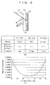
- Fig. 6 includes a view, a table, and a graph, illustrating a specific example according to the fourth form of implementation of the present invention.
- the abscissa axis represents the angle at which electromagnetic waves is incident on a solar cell and the ordinate axis represents the damping factor measured when the three medium layers of the solar cell, namely the top glass layer 51, the EVA (ethylene-vinyl-acetate) layer 52 and the semiconductor layer 53 are adjusted in thickness so that the effect of canceling the reflected waves each other is maximized for the frequencies in the UHF band.
- an electromagnetic-wave absorbing method using a solar cell in accordance with the present invention makes it possible to absorb electromagnetic waves without reflection thereof and without impeding solar light power generation. Consequently, applying an electromagnetic-wave absorbing method using a solar cell in accordance with the present invention to an existing solar cell system allows the solar cell system to generate power while preventing electromagnetic-wave troubles such as ghost images from coming about, thereby expediting the dissemination of solar cells and the preservation of global environments.
Landscapes
- Photovoltaic Devices (AREA)
- Aerials With Secondary Devices (AREA)
Abstract
An electromagnetic-wave absorbing method using a solar cell
or cells is provided, whereby there comes about essentially no
reflection of electromagnetic waves by the solar cell or cells without
impeding solar light power generation thereby. A solar cell module
(10) may be constructed from a plurality of solar cells (1) wherein
respective upper electrodes (2, 2) are electrically connected together
by a conductor (7) and a common lower electrode (6) is used. So that
any possibly reflected wave may be absorbed, the impedance of the
solar cells to electromagnetic waves incident thereon is matched to an
electromagnetic-wave characteristic impedance by adjusting the
number of the solar cells (1) arranged or the way in which they are
arranged or by connecting a capacitor (13) across a pair of output
terminals (8, 9) of the module. Alternatively, a plurality of such solar
cell modules (10) different in shape and/or surface area are arranged
in such a manner that reflected wave being reflected by the individual
solar cell modules differ in phase so that they may be canceled one by
another. Alternatively, it is possible to form an electromagnetic wave
reflector (54, 57) on a rear surface of the solar cell (1) or on a wall
surface over which it is to be mounted and a reticular
electromagnetic-wave reflector (55) on a top surface of the solar cell,
in an arrangement such that a reflected wave being reflected by the
electromagnetic-wave reflector (54, 57) on the rear surface or the wall
surface and a reflected wave being reflected by the reticular
electromagnetic-wave reflector (55) may interfere with each other and
be thereby cancelled each by other.
Description
- The present invention relates to electromagnetic-wave absorbing methods using a solar cell or cells and in particular to methods of absorbing electromagnetic waves with a solar cell or cells whereby there comes about essentially no reflection of electromagnetic waves without impeding solar light power generation by the solar cell or cells.
- As one of troubles associated with electromagnetic waves there is a so-called ghost phenomenon in which a TV image is doubled due to the fact that TV electromagnetic waves are reflected by a wall surface of a building such as a high-rise building or skyscraper.
- To get rid of such a ghost phenomenon, a measure can be taken in the reception side but basically it is important that the wall surfaces of such a high building be adapted not to reflect electromagnetic waves. Especially these days that the city is flooded with electromagnetic waves from cellular phones or the like, an unforeseen accident can be predicted and a technique of preventing electromagnetic waves from being reflected is being sought.
- In order to absorb TV electromagnetic waves in the VHF band, the use of a ferrite-type electromagnetic-wave absorbing wall having a ferrite tile embedded in a curtain wall has so far been proposed for a building wall surface. However, not only is the ferrite-type electromagnetic-wave absorbing wall inapplicable to absorbing electromagnetic waves in the UHF band, but also it is heavy in weight, and rather hard to construct practically and economically. For these reasons, the ferrite-type electromagnetic-wave absorber wall has scarcely come into wide use in general buildings.
- On the other hand, the utilization of solar energy in order to preserve the global environments intact makes progress to an extent that a solar cell panel is being laid on a general building wall. A solar cell made of Si (silicon), however, has entailed the problem that a solar cell acts as a reflector to electromagnetic waves and brings about an unanticipated ghost trouble, and hence the solar panel has not yet come into general use as expected.
- In view of the aforementioned problems in the prior art, the present invention has for its object to provide an electromagnetic wave absorbing method using a solar cell or cells, which can prevent the reflection of electromagnetic waves without impeding solar light power generation by the solar cell or cells.
- In order to achieve the object mentioned above, there is provided in accordance with the present invention a method of absorbing electromagnetic waves with a solar cell or cells, characterized by adjusting impedance of a solar cell to electromagnetic waves incident thereon so that there is virtually no reflection of the electromagnetic wave by the solar cell.
- In the method mentioned above, the impedance can be adjusted specifically by changing or adjusting the way in which the solar cells are wired together.
- In the method mentioned above, the impedance can also be adjusted specifically by appending a capacitor across output terminals of a solar cell module.
- In the method mentioned above, the impedance can also be adjusted specifically by appending an electronic component or components to the solar cell or cells internally or externally thereof.
- According to these electromagnetic-wave absorbing methods using a solar cell or cells, the impedance of the solar cell or cells is matched to an electromagnetic-wave characteristic impedance; hence there comes about virtually no reflection of an electric wave by the solar cell or solar cells.
- Since the energy of electromagnetic waves in the UHF and VHF ranges is lower than the absorption limit energy of a solar cell, a protective film and semiconductor layers making up a solar cell act as dielectrics for electromagnetic waves in the UHF and VHF ranges while a wiring conductor being metallic in the solar cell acts as a reflector. Changing the distribution of wiring conductors in solar cells changes the boundary condition for electromagnetic waves and changes the capacitance and inductance; hence that can be used to adjust the impedance of a solar cell to electromagnetic waves incident thereon. In order to change the distribution of wiring conductors in a solar cell module, the solar cells making up the module can be adjusted in their arrangement and then wired together. The impedance can also be adjusted by appending a capacitor across a pair of output terminals of the solar cell module, or by appending an electronic component such as a capacitor to a solar cell internally or externally thereof.
- These specific methods, none of which produces any short circuit condition for a direct current, exert no adverse influence on solar light power generation by the solar cell or cells while preventing electromagnetic waves from reflecting.
- There is also provided in accordance with the present invention a method of absorbing electromagnetic waves with a solar cell or cells, characterized by arranging a plurality of solar cell modules different in shape and/or surface area in such a manner that reflected waves from the individual solar cell modules vary in phase so that they are canceled one by another.
- According to this method which is designed to adjust the phases of reflected waves of incident electromagnetic waves advantageously in terms of the shape and/or surface areas of modules, the modules can be so arranged that the reflected waves may be formed which are opposite in phase to one another and can thus be cancelled one by another.
- In the method mentioned above, a plurality of solar cells can be connected together in the form of an antenna such as to absorb electromagnetic waves.
- Alternatively, a plurality of solar cells may be connected together in the form of a loop and a matching load may then be connected across loop ends of the loop.
- Alternatively, upper and lower electrodes of a plurality of solar cells may be connected respectively in series, and a matching load may then be connected across a pair of output terminals leading from such an upper and a lower electrode.
- According to the specific methods mentioned above, the solar cells are allowed to act as a loop antenna or a patch antenna and the matching load to act to absorb the electromagnetic energy; hence virtually no reflected wave is produced.
- The present invention also provides a method of absorbing electromagnetic waves with a solar cell or cells, characterized by adjusting respective thicknesses of various layers of a solar cell so that reflected waves reflected, respectively, by these layers interfere with one another and are thereby cancelled one by another.
- The present invention also provides a method of absorbing electromagnetic waves with a solar cell or cells, characterized by forming an solar cell with an electromagnetic-wave reflector on a rear surface thereof and with a reticular electromagnetic-wave reflector on a top surface thereof in an arrangement such that a reflected wave being reflected by the electromagnetic-wave reflector on the rear surface and a reflected wave being reflected by the reticular electromagnetic-wave reflector may interfere with each other and be thereby cancelled each by other.
- The present invention also provides a method of absorbing electromagnetic waves with a solar cell, characterized by forming an electromagnetic-wave reflector on a wall surface over which a solar cell is to be mounted and forming a reticular electromagnetic-wave reflector on a top surface of the solar cell, in an arrangement such that a reflected wave being reflected by the electromagnetic-wave reflector on the wall surface and a reflected wave being reflected by the reticular electromagnetic-wave reflector may interfere with each other and be thereby cancelled each by other.
- According to these methods, virtually no reflected wave is produced from electromagnetic waves incident on a solar cell on the one hand and power generation from solar light is possible on the other hand.
- The present invention will better be understood from the following detailed description and the drawings attached hereto showing certain illustrative forms of implementation of the present invention. In this connection, it should be noted that such forms of implementation illustrated in the accompanying drawings hereof are intended in no way to limit the present invention but to facilitate an explanation and understanding thereof. In the drawings:
- Fig. 1 is a typical cross sectional view illustrating a first form of implementation of the present invention;
- Fig. 2 is a diagram illustrating a second form of implementation of the present invention;
- Fig. 3 is a diagram of the vector representation of phase angles of reflected waves from a plurality of modules which differ in phase angle of reflection coefficient;
- Fig. 4 shows diagrams illustrating a third form of implementation of the present invention;
- Fig. 5 shows views illustrating a fourth form of implementation of the present invention; and
- Fig. 6 includes a view, a table, and a graph, illustrating a specific example according to the fourth form of implementation of the present invention.
-
- Hereinafter, the present invention will be described in detail with reference to suitable forms of implementation thereof illustrated in the drawing figures.
- At the outset, mention is made of a first form of implementation of the present invention. Fig. 1 is a typical cross sectional view illustrating a first form of implementation of the present invention. A
solar cell module 10 according to the present invention is made up of a plurality ofsolar cells 1 connected one to another by conductors 7 wherein eachsolar cell 1 comprises anupper electrode 2, atransparent electrode 3, a semiconductor p-layer 4, a semiconductor n-layer 5 and a lower electrode 6. In the example illustrated in the Figure, thesolar cells 1 are connected parallel to each other with theupper electrodes 2 in theadjacent cells 1 connected together and the lower electrode 6 used in common, and further with a capacitor 13 connected acrossoutput terminals 8 and 9 of the solar cell module, although the capacitor 13 may be omitted and thesolar cells 1 may be connected in series or connected both in series and parallel in any of various possible combinations. - By the way, when
electromagnetic waves 12 are incident on asolar cell 1, if the impedance of thesolar cell 1 when seen from theelectromagnetic waves 12 incident on thesolar cell 1 is expressed by Z, then its reflectivity τ for the solar cell is given by equation (1) as follows: - Changing the way in which the
solar cells 1 that make up thesolar cell module 10 as shown in Fig. 1 are wired together, changes the boundary condition for the electromagnetic waves, and therefore changes their conductance and inductance. Hence the impedance Z of thesolar cells 1 seen from theelectromagnetic waves 12 incident thereon can be adjusted by so changing or adjusting. Also, the impedance Z can be adjusted, e. g., by changing or adjusting the number of series- and/or parallel-connected solar cells. Further, the impedance can be adjusted by changing or adjusting the way in which a module or modules made of series-connected cells and a module or modules made of parallel-connected cells are combined together. Still further, the impedance Z can be adjusted more finely by changing or adjusting the way in which they are so combined when series-connected cells and parallel-connected cells are different in number. Yet further, the impedance Z can be adjusted by connecting a capacitor 13 acrossoutput terminals 8 and 9 of the module. Of course, such an electronic component as a capacitor may be attached to each of all or selected ones of thesolar cells 1 externally or internally thereof. The capacitor passes no direct current and hence exerts no influence on solar light power generation. If in any of these ways the impedance Z of the solar cell or cells is so adjusted that the same becomes equal to electromagnetic-wave characteristic impedance Z0, then the reflection coefficient τ becomes zero and virtually no reflection of the electromagnetic wave comes about. - Mention is next made of a second form of implementation of the present invention. Fig. 2 is a diagram illustrating a second form of implementation of the present invention. In the Figure,
reference numerals solar cell module 21 and the impedance of asolar module 22 are expressed by ZA and ZB, respectively, their respective reflection coefficients τA and τB are given by the following equations, respectively: Further, with their real parts and imaginary parts expressed as τZA and τZB; and τjZA and τjZB, respectively, the reflection coefficients τA and τB are given by equations (8) and (9) as follows:
solar cell module 21 and asolar cell module 22 are given by equations (10) and (11) as follows: - It follows, therefore, that if the impedances Za, Zb, Zaa, and Zbb of the
modules solar cell modules solar modules - The impedances Za, Zb, Zaa, and Zbb can be adjusted by changing or adjusting the areas of solar cell modules, the manner in which they are wired, and the way in which they are arranged, or upon additionally connecting an electronic component such as a capacitor to the modules internally or externally thereof.
- Fig. 3 is a diagram of the vector representation of phase angles of reflected waves from a plurality of modules which differ in phase angle in reflection coefficient. As shown, if a variety of
phase angles 31 exist, then there come to be made pairs of reflected waves which cancel each other and, as a result, virtually any reflected wave is no longer emitted. - Mention is next made of a third form of implementation of the present invention. Fig. 4 shows diagrams illustrating a third form of implementation of the present invention. In Fig. 4, there are shown at (a) a plurality of
solar cells 1 arranged in the form of a loop with their upper or lower electrodes connected in series and with a matchingload 41 such as, for example, a capacitor connected across their loop ends. - According to this arrangement, the solar cells act as a loop antenna and the electromagnetic energy is absorbed in the matching
load 41; hence virtually no reflected wave is emitted. - Fig. 4 also shows at (b) a plurality of
solar cells 1 arranged in a zigzag form with both their upper and lower electrodes are connected in series, respectively. - According to this arrangement, wherein the solar cells act as a patch antenna and have matching
loads 41 connected thereto as shown to absorb the electromagnetic energy, virtually no reflected light is emitted. - Mention is next made of a fourth form of implementation of the present invention. Fig. 5 has views illustrating a fourth form of implementation of the present invention.
- Fig. 5 shows at (a) an embodiment in which the three medium layers of a solar cell, viz., a
top glass layer 51, an EVA (ethylene-vinyl acetate)layer 52 and asemiconductor layer 53, have their respective thicknesses controlled or adjusted so that reflected waves reflected on their respective surfaces are opposite in phase. According to this arrangement, wherein reflected waves reflected on their respective surfaces are made opposite in phase, the reflected waves are canceled each by other. - Fig. 5 shows at (b) another embodiment in which a solar cell is coated on its rear surface with an electromagnetic-wave reflecting
metallic film 54 and formed over its front surface with a reticular, electromagnetic-wave reflectingmetallic film 55. Here, the spacing between the electromagnetic-wave reflectingmetallic film 54 on the rear surface and the reticular, electromagnetic-wave reflecting film 55 is adjusted to cause a reflected wave reflected by the electromagnetic-wave reflecting film 54 on the rear surface and a reflected wave reflected by the reticular, electromagnetic-wave reflecting film 55 to interfere with each other, thereby canceling them each other. According to this embodiment, not only is emitted essentially no reflected wave, but also the incident solar light transmitting through the reticular, electromagnetic-wave reflecting film 55 can be used to generate electric power. - Fig: 5 shows at (c) a further embodiment in which a
wall surface 56 over which a solar cell is to be disposed is provided with areflector 57 for electromagnetic waves. In this embodiment, the spacing between thereflector 57 and the rear surface of the solar cell is adjusted so that the reflected wave from thereflector 57 and the reflected wave from the solar cell surface are opposite in phase to each other. According to this embodiment, these reflected waves cancel each other, and virtually no reflected wave is thus emitted. - Mention is next made of a specific example of the present invention. Fig. 6 includes a view, a table, and a graph, illustrating a specific example according to the fourth form of implementation of the present invention. In the graph, the abscissa axis represents the angle at which electromagnetic waves is incident on a solar cell and the ordinate axis represents the damping factor measured when the three medium layers of the solar cell, namely the
top glass layer 51, the EVA (ethylene-vinyl-acetate)layer 52 and thesemiconductor layer 53 are adjusted in thickness so that the effect of canceling the reflected waves each other is maximized for the frequencies in the UHF band. - As will be appreciated from the foregoing description, an electromagnetic-wave absorbing method using a solar cell in accordance with the present invention makes it possible to absorb electromagnetic waves without reflection thereof and without impeding solar light power generation. Consequently, applying an electromagnetic-wave absorbing method using a solar cell in accordance with the present invention to an existing solar cell system allows the solar cell system to generate power while preventing electromagnetic-wave troubles such as ghost images from coming about, thereby expediting the dissemination of solar cells and the preservation of global environments.
Claims (11)
- A method of absorbing electromagnetic waves with a solar cell or cells, characterized by adjusting impedance of a solar cell to electromagnetic waves incident thereon so that there comes about virtually no reflection of the electromagnetic waves by the solar cell.
- A method of absorbing electromagnetic waves with a solar cell or cells as set forth in claim 1, characterized in that the impedance is adjusted by changing the way in which the solar cells are wired together.
- A method of absorbing electromagnetic waves with a solar cell or cells as set forth in claim 1, characterized in that the impedance is adjusted by appending a capacitor across output terminals of a solar cell module.
- A method of absorbing electromagnetic waves with a solar cell or cells as set forth in claim 1, characterized in that the impedance is adjusted by appending an electronic component or components to the solar cell or cells internally or externally thereof.
- A method of absorbing electromagnetic waves with a solar cell or cells, characterized by arranging a plurality of solar cell modules different in shape and/or surface area in such a manner that reflected waves from the individual solar cell modules vary in phase so that they are canceled one by another.
- A method of absorbing electromagnetic waves with a solar cell or cells, characterized by connecting a plurality of solar cells together in the form of an antenna such as to absorb electromagnetic waves.
- A method of absorbing electromagnetic waves with a solar cell or cells as set forth in claim 6, characterized by connecting a plurality of solar cells together in the form of a loop and connecting a matching load across loop ends of the loop.
- A method of absorbing electromagnetic waves with a solar cell or cells as set forth in claim 6, characterized by providing a plurality of solar cells having upper and lower electrodes which are connected in series, respectively, and connecting a matching load across a pair of output terminals leading from such an upper and a lower electrode, respectively.
- A method of absorbing electromagnetic waves with a solar cell or cells, characterized by adjusting respective thicknesses of various layers of a solar cell so that reflected waves reflected, respectively, by these layers interfere with one another and are thereby cancelled one by another.
- A method of absorbing electromagnetic waves with a solar cell or cells, characterized by forming an solar cell with an electromagnetic-wave reflector on a rear surface thereof and with a reticular electromagnetic-wave reflector on a top surface thereof in an arrangement such that a reflected wave being reflected by the electromagnetic-wave reflector on the rear surface and a reflected wave being reflected by the reticular electromagnetic-wave reflector may interfere with each other and be thereby cancelled each by other.
- A method of absorbing electromagnetic waves with a solar cell, characterized by forming an electromagnetic reflector on a wall surface over which a solar cell is to be mounted and forming a reticular electromagnetic-wave reflector on a top surface of the solar cell, in an arrangement such that a reflected wave being reflected by the electromagnetic-wave reflector on the wall surface and a reflected wave being reflected by the reticular electromagnetic-wave reflector may interfere with each other and be thereby cancelled each by other.
Applications Claiming Priority (3)
| Application Number | Priority Date | Filing Date | Title |
|---|---|---|---|
| JP2001135424A JP4009893B2 (en) | 2001-05-02 | 2001-05-02 | Electromagnetic wave absorption method using solar cell |
| JP2001135424 | 2001-05-02 | ||
| PCT/JP2002/004392 WO2002091481A1 (en) | 2001-05-02 | 2002-05-02 | Method for absorbing electromagnetic wave using solar cell |
Publications (1)
| Publication Number | Publication Date |
|---|---|
| EP1465261A1 true EP1465261A1 (en) | 2004-10-06 |
Family
ID=18982892
Family Applications (1)
| Application Number | Title | Priority Date | Filing Date |
|---|---|---|---|
| EP20020724678 Withdrawn EP1465261A1 (en) | 2001-05-02 | 2002-05-02 | Method for absorbing electromagnetic wave using solar cell |
Country Status (4)
| Country | Link |
|---|---|
| US (1) | US20040140003A1 (en) |
| EP (1) | EP1465261A1 (en) |
| JP (1) | JP4009893B2 (en) |
| WO (1) | WO2002091481A1 (en) |
Families Citing this family (3)
| Publication number | Priority date | Publication date | Assignee | Title |
|---|---|---|---|---|
| JP2008029125A (en) * | 2006-07-21 | 2008-02-07 | Sony Corp | Electromagnetic induction processing equipment |
| JP2010258158A (en) * | 2009-04-23 | 2010-11-11 | Sharp Corp | Wiring sheet, solar cell with wiring sheet and solar cell module |
| DE102009044610A1 (en) * | 2009-11-20 | 2011-05-26 | Azur Space Solar Power Gmbh | solar cell module |
Family Cites Families (9)
| Publication number | Priority date | Publication date | Assignee | Title |
|---|---|---|---|---|
| JPH0236318Y2 (en) * | 1985-06-21 | 1990-10-03 | ||
| JPH0642563B2 (en) * | 1988-11-24 | 1994-06-01 | 日本碍子株式会社 | Solar panel |
| JPH06237091A (en) * | 1993-02-08 | 1994-08-23 | Hitachi Eng Co Ltd | Radio frequency anechoic enclosure |
| EP0632507A3 (en) * | 1993-05-12 | 1995-11-22 | Optical Coating Laboratory Inc | Cover for solar cells which reflects UV / IR rays. |
| JPH08253913A (en) * | 1995-03-15 | 1996-10-01 | Fujita Corp | Solar panel integrated sound insulation panel |
| JPH11150393A (en) * | 1997-11-14 | 1999-06-02 | Oji Toobi Kk | Transparent radio wave absorber and method for producing the same |
| JP2000049487A (en) * | 1998-07-29 | 2000-02-18 | Hitachi Ltd | Electromagnetic wave absorbing method, electromagnetic wave absorbing device, electronic component and electronic device |
| DE19938199C1 (en) * | 1999-08-12 | 2001-01-25 | Inst Solare Energieversorgungstechnik Iset | Solar-powered HF transmitter and/or receiver has antenna element for transmission and/or reception antenna provided by solar cell contact |
| US6590150B1 (en) * | 2001-05-11 | 2003-07-08 | Karl F. Kiefer | Combination photovoltaic cell and RF antenna and method |
-
2001
- 2001-05-02 JP JP2001135424A patent/JP4009893B2/en not_active Expired - Fee Related
-
2002
- 2002-05-02 US US10/476,616 patent/US20040140003A1/en not_active Abandoned
- 2002-05-02 WO PCT/JP2002/004392 patent/WO2002091481A1/en not_active Ceased
- 2002-05-02 EP EP20020724678 patent/EP1465261A1/en not_active Withdrawn
Non-Patent Citations (1)
| Title |
|---|
| See references of WO02091481A1 * |
Also Published As
| Publication number | Publication date |
|---|---|
| JP4009893B2 (en) | 2007-11-21 |
| JP2002329882A (en) | 2002-11-15 |
| WO2002091481A1 (en) | 2002-11-14 |
| US20040140003A1 (en) | 2004-07-22 |
Similar Documents
| Publication | Publication Date | Title |
|---|---|---|
| US8338772B2 (en) | Devices, systems, and methods for harvesting energy and methods for forming such devices | |
| FR2661782A1 (en) | DIPOLE NETWORK ANTENNA WITH DUAL POLARIZATION. | |
| Li et al. | Frequency selective radome with wide diffusive bands | |
| US6395971B1 (en) | Apparatus for converting solar energy into electrical energy and for radiating and/or receiving high frequency electromagnetic waves | |
| Ragulis et al. | Shielding effectiveness of modern energy-saving glasses and windows | |
| US11881624B2 (en) | Wireless communication system and method | |
| CN113451784B (en) | High-performance packaging radiation absorber | |
| Hamid et al. | Thin multilayer frequency selective surface absorber with wide absorption response | |
| JPS59207703A (en) | Microstrip antenna | |
| EP3958400B1 (en) | System and method for diffraction of electromagnetic wave | |
| US20040140003A1 (en) | Method for absorbing electromagnetic wave using solar cell | |
| JP6965989B2 (en) | Electromagnetic wave propagation control member, electromagnetic wave propagation control structure, sash with electromagnetic wave propagation control member, and window structure | |
| US6424308B1 (en) | Wideband matching surface for dielectric lens and/or radomes and/or absorbers | |
| Zhong et al. | Broadband meta-surface with polarization-insensitive and wide-angle for electromagnetic energy harvesting | |
| CN109103609B (en) | An integrated antenna and array integrating solar cells | |
| Hamid et al. | Design and oblique incidence performance of a planar radome absorber | |
| RS20130320A1 (en) | PHOTO VOLTAGE ELEMENT WITH RESONATOR | |
| CN115615556B (en) | A mid-infrared pyroelectric detector based on metasurface integration | |
| Chueca et al. | Modelling of frequency selective surfaces on multi-layered glazing windows | |
| US3680133A (en) | Subsurface traveling wave antenna | |
| Mahesh et al. | A wideband resistive beam-splitter screen | |
| Sarehraz | Novel rectenna for collection of infrared and visible radiation | |
| Loecker et al. | Metamaterial enhanced phased-array antenna | |
| JP2005117060A (en) | Electromagnetic wave absorption method using solar cell | |
| Maniotis et al. | Design of an ultra-thin bandwidth-optimized metamaterial absorber for EMC applications |
Legal Events
| Date | Code | Title | Description |
|---|---|---|---|
| PUAI | Public reference made under article 153(3) epc to a published international application that has entered the european phase |
Free format text: ORIGINAL CODE: 0009012 |
|
| 17P | Request for examination filed |
Effective date: 20031127 |
|
| AK | Designated contracting states |
Kind code of ref document: A1 Designated state(s): AT BE CH DE ES GB LI |
|
| STAA | Information on the status of an ep patent application or granted ep patent |
Free format text: STATUS: THE APPLICATION IS DEEMED TO BE WITHDRAWN |
|
| 18D | Application deemed to be withdrawn |
Effective date: 20081201 |