EP1460638A2 - Semiconductor memory device with shift register-based refresh address generation circuit - Google Patents
Semiconductor memory device with shift register-based refresh address generation circuit Download PDFInfo
- Publication number
- EP1460638A2 EP1460638A2 EP04005805A EP04005805A EP1460638A2 EP 1460638 A2 EP1460638 A2 EP 1460638A2 EP 04005805 A EP04005805 A EP 04005805A EP 04005805 A EP04005805 A EP 04005805A EP 1460638 A2 EP1460638 A2 EP 1460638A2
- Authority
- EP
- European Patent Office
- Prior art keywords
- refresh
- signal
- cell array
- shift
- memory device
- Prior art date
- Legal status (The legal status is an assumption and is not a legal conclusion. Google has not performed a legal analysis and makes no representation as to the accuracy of the status listed.)
- Granted
Links
Images


Classifications
-
- G—PHYSICS
- G11—INFORMATION STORAGE
- G11C—STATIC STORES
- G11C11/00—Digital stores characterised by the use of particular electric or magnetic storage elements; Storage elements therefor
- G11C11/21—Digital stores characterised by the use of particular electric or magnetic storage elements; Storage elements therefor using electric elements
- G11C11/34—Digital stores characterised by the use of particular electric or magnetic storage elements; Storage elements therefor using electric elements using semiconductor devices
- G11C11/40—Digital stores characterised by the use of particular electric or magnetic storage elements; Storage elements therefor using electric elements using semiconductor devices using transistors
- G11C11/401—Digital stores characterised by the use of particular electric or magnetic storage elements; Storage elements therefor using electric elements using semiconductor devices using transistors forming cells needing refreshing or charge regeneration, i.e. dynamic cells
- G11C11/406—Management or control of the refreshing or charge-regeneration cycles
Landscapes
- Engineering & Computer Science (AREA)
- Microelectronics & Electronic Packaging (AREA)
- Computer Hardware Design (AREA)
- Dram (AREA)
Abstract
Description
- The present invention relates to a semiconductor memory device, and more particularly to a semiconductor memory device with a function of refreshing stored data.
- A class of semiconductor memory devices such as dynamic random-access memories (DRAMs) store each data bit in the form of a charge on a very small capacitor. Because of the presence of leakage current from capacitors, the stored data cannot be retained indefinitely. The lost capacitor charge must be restored at appropriate intervals by rewriting the same data. This restoration operation is called "refresh."
- Existing semiconductor memory devices have an internal address counter to generate refresh address, which is typically a binary counter to produce binary address. This is, however, not always an efficient way. In the case the actual memory size cannot be represented in the form of 2n, the address counter would produce useless address values after it has reached the maximum real memory address.
- One technique to overcome the above inefficiency in refresh address generation is to use shift registers. Specifically, the semiconductor memory device contains shift registers corresponding to individual word lines of each memory cell array. In refresh cycles, those shift registers successively generate a series of refresh addresses, thus scanning all word lines efficiently. (See, for example, the Japanese Patent Application Publication No.2000-311487, pages 4 and 5, Figs. 1 to 3.)
- We should, however, note that the conventional semiconductor memory devices described above are designed to distribute common control signals to all shift registers when updating refresh address. Since the number of shift registers increases in proportion to memory capacity, the power consumption in driving those control signals would be a problem.
- In view of the foregoing, it is an object of the present invention to provide a semiconductor memory device with low power consumption in driving control signals of shift registers.
- To accomplish the above object, the present invention provides a semiconductor memory device with a function of refreshing stored data. This semiconductor memory device comprises the following element: (a) a plurality of cell arrays, each composed of a predetermined number of rows of memory cells; (b) a plurality of sets of shift registers; and (c) a plurality of shift register controllers. The nth set of shift registers successively activate word line selection signals according to a given control signal, so as to refresh corresponding word lines of the nth cell array. The nth shift register controller provides the control signal to the nth set of shift registers when the nth cell array is being refreshed. When the refresh of the nth cell array is finished, the nth shift register controller forwards the control signal to the (n+1)th set of shift registers.
- The above and other objects, features and advantages of the present invention will become apparent from the following description when taken in conjunction with the accompanying drawings which illustrate preferred embodiments of the present invention by way of example.
-
- FIG. 1 is a conceptual view of a semiconductor memory device according to the present invention.
- FIG. 2 is a schematic circuit diagram of a semiconductor memory device according to a first embodiment of the invention.
- FIG. 3 is a schematic circuit diagram of a word line decoder.
- FIG. 4 is a schematic circuit diagram of a shift register.
- FIG. 5 is a schematic circuit diagram of a shift switch.
- FIG. 6 is a schematic circuit diagram of an RBLK latch.
- FIG. 7 is a schematic circuit diagram of a shift command generator.
- FIG. 8 is a timing diagram which shows how the control is passed from one cell array to another in refresh operation.
- FIG. 9 shows a critical path that must be followed to initiate refresh operation.
- FIG. 10 is a timing diagram explaining a critical path that must be followed to initiate refresh operation.
- FIG. 11 is a schematic circuit diagram of a semiconductor memory device according to a second embodiment of the invention.
- FIG. 12 is a schematic circuit diagram of a semiconductor memory device according to a third embodiment of the invention.
- FIG. 13 shows the entry to and exit from partial refresh mode and explains how refresh loops are created.
- FIG. 14 is a table showing the relationship between refresh areas shown in FIG. 13 and refresh intervals.
- FIG. 15 is a schematic circuit diagram of a semiconductor memory device according to a fourth embodiment of the invention.
- FIG. 16 shows the entry to and exit from partial refresh mode and explains how refresh loops are created.
- FIGS. 17A and 17B are tables showing the relationship between the refresh areas shown in FIG. 16 and refresh intervals.
- Preferred embodiments of the present invention will be described below with reference to the accompanying drawings, wherein like reference numerals refer to like elements throughout.
- FIG. 1 shows the concept of a semiconductor memory device according to the present invention, with a focus on the circuit for refreshing memory data. While the device actually has many sets of memory cell arrays, shift registers, and shift register controllers, FIG. 1 only shows a couple of instances for the sake of brevity. They are:
cell arrays 1a and 1b,shift registers 2a(0) to 2a(n) and 2b(0) to 2b(n), and shiftregister controllers - Note that the reference numerals have different suffixes "a," "b," and "c" to indicate each individual circuit group related to a particular memory cell array. For better readability, we may use the numeral "1" to collectively refer to the cell arrays, where appropriate. Likewise, the shift registers are collectively referred to by the numeral "2," and the shift register controllers are collectively referred to by the numeral "4."
- Referring to FIG. 1, the
cell arrays 1 are blocks of memory cells arranged in matrix form, each containing a predetermined number of rows. Thecell arrays 1 have multiple word lines WL0 to WLn for selection of a particular word in them.Shift registers 2 are attached to thosecell arrays 1, one for each word line WL0 to WLn. Theshift registers 2 are cascaded; i.e., the output of one register is connected to the input of the next register. In memory refresh cycles, word lines WL0 to WLn are activated one by one to cause data stored in each word to be refreshed. Theshift registers 2 receive such a word line selection signal from the previous stage and send it to the next stage, according to control signals CNTRa, CNTRb, and the like, which are given by the corresponding shift register controllers 4. - The shift register controllers 4 serve their
corresponding cell arrays 1 by providing control signal (e.g., CNTRa, CNTRb) to their corresponding sets ofshift registers 2. When onecell array 1 is all refreshed, its local shift register controller 4 stops sending the control signal and, instead, passes that signal to the succeeding set ofshift registers 2, so that thenext cell array 1 will be refreshed. - The semiconductor memory device of FIG. 1 operates as follows. Suppose, for example, that the cell array 1a is currently the subject of refresh. To successively activate word lines WL0 to WLn and select a word to be refreshed, the
shift registers 2a(0) to 2a(n) forward an active selection signal from stage to stage according to a control signal CNTRa given from theshift register controller 4a. When refresh of this cell array 1a is completed, theshift register controller 4a stops supplying the control signal CNTRa to theshift registers 2a(0) to 2a(n). Then anothershift register controller 4b outputs its control signal CNTRB to its local set ofshift registers 2b(0) to 2b(n) so that thecell array 1b will be refreshed next. Theshift registers 2b (1) to 2b(n) forward an active selection signal from stage to stage according to the control signal CNTRb from theshift register controller 4b, thus successively activating word lines WL0 to WLn of thecell array 1b to select a particular word to be refreshed. - As can be seen from the above, the present invention assigns a shift register controller 4 to each set of
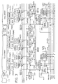
shift registers 2 coupled to acell array 1. The shift registers 2 convey a word line selection signal from stage to stage, according to control signals CNTRa, CNTRb, and the like from the corresponding shift register controller 4, thereby driving word lines WL0 to WLn successively to select each word to be refreshed. The proposed refresh mechanism only requires a single set of shift registers to work simultaneously, during which the other sets of shift registers need no clocks. That is, the present invention limits the number of shift register control signals CNTRa, CNTRb, and the like, which actually consume electric current. - This section describes a first embodiment of the present invention. FIG. 2 is a schematic circuit diagram showing a part of a semiconductor memory device according to a first embodiment of the invention. The illustrated semiconductor memory device comprises the following elements: cell arrays 11x, 11a, 11b, and so on (collectively referred to by the numeral "11"); sense amplifiers 12a, 12b, and so on (collectively "12"); word line decoders (MWLDEC) 13a(0) to 13a (63) , 13b (0) , 13b (1) , and so on (collectively "13"); word line drivers (MWLDRV) 15a(0) to 15a(64), 15b(0), 15b(1), and so on (collectively "15"); redundancy circuits (RDN) 17a(0) to 17a (64), 17b (0), 17b(1), and so on (collectively "17"); shift registers 19a(1) to 19a(64), 19b(1), 19b(2), and so on (collectively "19"); shift switches 21x, 21a, and so on (collectively "21"); row block (RBLK) latches 22a, 22b, and so on (collectively "22"); shift command generators 23a, 23b, and so on (collectively "23"); control signal generators 24a, 24b, and so on (collectively "24").
- The cell arrays 11 are blocks of memory cells arranged in matrix form, each containing a predetermined number of rows (word lines). Memory words in each cell array 11 are selected by a combination of main word line address and subordinate word line address. The main word lines of the illustrated
cell array 11a are driven by a set ofword line drivers 15a(0) to 15a(64), while those of thenext cell array 11b are driven by another set ofword line drivers 15b(0) to 15b(64) (not all shown). - The sense amplifiers 12 detect and amplify a voltage that appears at each bit line of the corresponding cell arrays 11. Each set of sense amplifiers 12 is shared by two neighboring cell arrays. In the example of FIG. 2, the
sense amplifiers 12b are shared by twocell arrays cell array 11a is being refreshed. In this case thecorresponding sense amplifiers 12a detect and amplify bit line voltages of thecell array 11a, and so do the subsequent set ofsense amplifiers 12b. - Each cell array 11 is assigned a dedicated set of word line decoders 13. In FIG. 2, a first set of
word line decoders 13a(0) to 13a(63) serve thecell array 11a, while a second set ofword line decoders 13b(0), 13b(1) , and the like serve thecell array 11b. - The
word line decoders 13a(0) to 13a(63) receive address switching signals SREFCXa and SREFCZa from theRBLK latch 22a and normal address signals RAAZ0 to RAAZ7 and RABZ0 to RABZ7 from other source. The leftmostword line decoder 13a(0) in FIG. 2 further receives a refresh signal REFA00a from the precedingshift switch 21x. The nextword line decoder 13a(1) receives a refresh signal REFA01a from the first-stage shift register 19a(1). Other decoders each receive refresh signals in a similar way, and the lastword line decoder 13a (63) receives a refresh signal REFA63a from theshift register 19a (63). - Address switching signals SREFCXa, SREFCZa, SREFCXb, and SREFCZb indicate the presence of an internal refresh request or a data read/write request from the external circuit. Normal address signals RAAZ0 to RAAZ7 and RABZ0 to RABZ7 represent a lower and upper address inputs given by external circuitry, respectively. Refresh signals REFA00a to REFA63a are used to drive main word lines of the
cell array 11a to refresh the memory cells on those lines. Refresh signals REFA00b, REFA01b, and so on are used to drive main word lines of thecell array 11b to refresh the corresponding cells. - Depending on the state of the address switching signals SREFCXa and SREFCZa, the
word line decoders 13a(0) to 13a(63) choose and decode either the normal address signals RAAZ0 to RAAZ7 and RABZ0 to RABZ7 or the refresh signals REFA00a to REFA63a, thus supplying theircorresponding redundancy circuit 17a(0) to 17a(64) with signals to drive main word lines of thecell array 11a. Suppose, for example, that the address switching signal SREFCXa and its complementary counterpart SREFCZa indicate the presence of a refresh request (i.e., SREFCXa is low, while SREFCZa is high). In this case, theword line decoders 13a(0) to 13a(63) provide their associatedredundancy circuits 17a(0) to 17a(64) with a signal for driving one main word line as specified by the refresh signals REFA00a to REFA63a. When, in turn, the address switching signals SREFCXa and SREFCZa indicate the presence of a data read/write request (i.e., SREFCXa is high, while SREFCZa is low), theword line decoders 13a(0) to 13a(63) decode the given normal address signals RAAZ0 to RAAZ7 and RABZ0 to RABZ7, thus supplying main word line driving signals to their associatedredundancy circuits 17a(0) to 17a(64). - The next set of
word line decoders 13b(0) to 13b(63) (not all shown) operate similarly to theword line decoders 13a(0) to 13a(63) described above. That is, they either decode normal address signals RAAZ0 to RAAZ7 and RABZ0 to RABZ7 or activate themselves according to given refresh signals REFA00b, REFA01b, and so on, depending on the state of address switching signals SREFCXb and SREFCZb provided from theRBLK latch 22b. Their outputs are supplied to theredundant circuits 17b(0) to 17b(65) to drive main word lines of thecell array 11b. - FIG. 3 is a schematic circuit diagram showing an example of word line decoder structure. The illustrated
word line decoder 13a(0) is composed of transistors M1(1) and M1(2), M2, M3, and M4. All transistors are n-channel MOSFETs. - Three transistors M1 (1) , M1 (2) , and M2 are connected in series, and the drain of the topmost transistor M1(1) is wired to the
redundancy circuits 17a(0) and 17a(1) through the line named PMWLX. " Given to the gate of transistor M1 (1) is one of the lower normal address signals RAAZ0 to RAAZ7. Likewise, the gate of transistor M1 (2) is driven with one of the upper normal address signals RABZ0 to RABZ7. Only a particular combination of upper and lower address signals will turn on the transistors M1 (1) and M1 (2) simultaneously, thus closing the series circuit. - The gate of the transistor M2 is driven by an address switching signal SREFCXa. Connected to its source terminal is BKEX, a voltage supplied when either the normal address signals RAAZ0 to RAAZ7 and RABZ0 to RABZ7 or the refresh signal REFA00a is valid. When the address switching signal SREFCXa goes high (i.e., when there is a data read/write request), the transistor M2 turns on its source-drain channel. The transistor M4 turns off at this moment, since another address switching signal SREFCZa (which is complementary to SREFCXa) becomes low.
- In operation, the transistors M1(1) and M1(2) and M2 will all turn on when the address switching signal SREFCXa is in a high state to indicate the presence of a data read/write request, and only when the normal address signals RAAZ0 to RAAZ7 and RABZ0 to RABZ7 match with a predefined pattern. This condition results in a voltage BKEX appearing at the drain of transistor M1 (1). BKEX is the delivered to the
redundancy circuits 17a(0) and 17a (1) for use as a word-line driving signal PMWLX, which selects a particular word in thecell array 11a. - Referring now to the right half of FIG. 3, the source terminal of transistor M3 is connected to the drain of transistor M4, and the gate of same is driven by a refresh signal REFA00a. The drain of transistor M3 is connected together with the drain of transistor M1(1). Transistor M4, on the other hand, receives an address switching signal SREFCZa at its gate terminal. Connected to its source terminal is BKEX, a voltage that becomes available when refresh signal REFA00a is valid.
- In operation, the two transistors M3 and M4 will turn on when the address switching signal SREFCXa is in a high state to indicate the presence of a refresh request, and only when the refresh signal REFA00a is active. This causes the voltage BKEX to appear at the drain of transistor M3, which is then supplied to the
redundancy circuits 17a(0) and 17a(1) for use as a word-line driving signal PMWLX. - The other
word line decoders 13a(1) to 13a(63) shown in FIG. 2 are configured in the same way as theword line decoder 13a(0) described above, except that their transistors M1 (1) and M1 (2) are activated by different combinations of normal address signals, and that their respective transistors M3 are controlled by different refresh signals REFA01a, REFA02a, ...REFA63a. That is, only one of theword line decoders 13a(0) to 13a(63) is allowed to activate a main word line with its word-line driving signal PMWLX, when a particular pattern of normal address signals RAAZ0 to RAAZ7 and RABZ0 to RABZ7 are given. The same is applied to otherword line decoders 13b(0), 13b (1) , and the like, for which we will omit the explanation. - Referring back to FIG. 2, the memory device has a dedicated set of word line drivers 15 for each cell array 11. Specifically, one set of
word line drivers 15a(0) to 15a(64) are attached to thecell array 11a, and another set ofword line drivers 15b(0) to 15b(64) (not all shown) are attached to thesubsequent cell array 11b. Theword line drivers 15a(0) to 15a(64) receive the output signals of theword line decoders 13a(0) to 13a(63) via thecorresponding redundancy circuits 17a(0) to 17a(64), and use them to drive main word lines of thecell array 11a. Similarly, theword line drivers 15b(0) to 15b(64) receive the output signals ofword line decoders 13b(0) to 13b(63) (not all shown) via thecorresponding redundancy circuits 17b (0) to 17b(64) (not all shown). Those signals are used to drive the main word lines of thecell array 11b. - The purpose of the intervening redundancy circuits 17 is to repair a defect found in the memory cells. The output of each word line decoder 13 is connected to two redundancy circuits 17. If a defective memory cell is found on a certain main word line, the relevant redundancy circuits 17 configure themselves to route the word line driving signal from the corresponding word line decoder 13 to a different word line driver 15. Suppose, for example, that the
cell array 11a has a defective cell on the first main word line that theword line driver 15a(0) drives. Theredundancy circuit 17a(0) disables its associatedword line driver 15a(0) while causing the nextredundant circuit 17a(1) to supply theword line driver 15a(1) with a main word line driving signal from theword line decoder 13a(0). - Each cell array 11 is given a set of shift registers 19. Specifically,
shift registers 19a(1) to 19a(64) serve thecell array 11a, and another set ofshift registers 19b(1) to 19b(64) (not all shown) serve thenext cell array 11b. The former set ofshift registers 19a(1) to 19a(64) are each allocated to a particular main word line of thecell array 11a. Likewise, the latter set ofshift registers 19b(1) to 19b(64) are each allocated to a particular main word line of thecell array 11b. - The
shift registers 19a(1) to 19a(64) operate under the control of their localshift command generator 23a. In synchronization with subordinate shift command signals SSFTXa and SSFTZa given from theshift command generator 23a, theshift registers 19a(1) to 19a(64) successively produce refresh signals REFA01a to REFA64a. The seed of those signals is a refresh signal REFA00a sent from the precedingshift switch 21x. Note that the refresh signals REFA01a to REFA64a become active only one at a time. - The next set of
shift registers 19b(1) to 19b(64) (not all shown) operate in a similar way to theshift registers 19a(1) to 19a(64) described above. That is, they successively produce refresh signals REFA01b to REFA64b (not all shown) in synchronization with subordinate shift command signals SSFTXb and SSFTZb supplied from their localshift command generator 23b, with a seed refresh signal REFA00b received from the precedingshift switch 21a. - FIG. 4 is a schematic circuit diagram showing an example of shift register structure. The illustrated
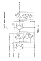
shift register 19a(1) is composed of twotransfer gates latch circuits first latch circuit 32 could change the initial state of REFA01a to low level, without affecting the structure of the other part. - The
first transfer gate 31 is composed of two transistors M5 and M6, the former being a p-channel MOSFET, and the latter being an n-channel MOSFET. A subordinate shift command signal SSFTZa is applied to the gate of one transistor M5, while its complementary counterpart SSFTXa is given to the gate of the other transistor M6. Thistransfer gate 31 transfers a given refresh signal REFA00a from the precedingshift switch 21x to thelatch circuit 32 in response to the subordinate shift command signals SSFTXa and SSFTZa. - The
first latch circuit 32 is composed of an inverter Z1, a NAND gate Z2, and two transistors T1 and T2. Given to one input of the NAND gate Z2 is an initialization signal CLRNX, which is one of the miscellaneous control signals CSIG shown in FIG. 2. Thislatch circuit 32 captures and holds the refresh signal REFA00a from thetransfer gate 31, making it available to thesubsequent transfer gate 33. If an initialization signal CLRNX is given to the NAND gate Z2, thelatch circuit 32 clears the latched state of REFA00a, thus sending a low level signal to thetransfer gate 33. Transistors T1 (p-channel MOSFET) and T2 (n-channel MOSFET) are attached to the NAND gate Z2. Both transistors T1 and T2 turn off when thetransfer gate 31 is active, thus disabling the NAND gate Z2 from driving its load. This additional circuit ensures reliable signal transfer operation from thetransfer gate 31 to thelatch circuit 32. - The
second transfer gate 33 is composed of two transistors M7 and M8, the former being an n-channel MOSFET, and the latter being a p-channel MOSFET. The subordinate shift command signal SSFTZa is given to the gate of one transistor M7, while its complementary counterpart SSFTXa is given to the gate of the other transistor M8. Thistransfer gate 33 supplies thesecond latch circuit 34 with the refresh signal held in thefirst latch circuit 32, in response to the subordinate shift command signals SSFTXa and SSFTZa. The twotransfer gates - The
second latch circuit 34 is formed from two inverters Z3 and Z4 and two transistors T3 and T4.. Thislatch circuit 34 captures and holds the refresh signal REFA00a from thetransfer gate 33, and supplies it to thesubsequent shift register 19a(1) as a refresh signal REFA01a. Optionally, thesecond latch circuit 34 may have the same structure as thefirst latch circuit 32. Transistors T3 (p-channel MOSFET) and T4 (n-channel MOSFET) are attached to the inverter Z4 in thelatch circuit 34. Both transistors T3 and T4 turn off when thetransfer gate 33 is active, thus disabling the inverter Z4 from driving its load. This additional circuit ensures reliable signal transfer operation from thetransfer gate 33 to thelatch circuit 34. - Subordinate shift command signals SSFTXa and SSFTZa are a complementary pair of clock signals alternating between high and low states. In the first half cycle of SSFTXa and SSFTZa, a given refresh signal REFA00a is transferred from the preceding
shift switch 21x to thefirst latch circuit 32 through thefirst transfer gate 31 that is turned on. In the second half cycle of SSFTXa and SSFTZa, thefirst transfer gate 31 is closed, whereas thesecond transfer gate 33 is opened. Accordingly, the refresh signal REFA00a held at thefirst latch circuit 32 is passed to thesecond latch circuit 34, which is then supplied to the subsequent shift register as a refresh signal REFA01a. - While we have concentrated on the
first shift register 19a(1), the same principle is applied to all theother shift registers 19a(2), 19a(3), and so on. We will therefore omit the explanation of those registers here. - Referring back to FIG. 2, the shift flag signal FLAG indicates whether the refresh of subordinate word lines has finished in each cell array 11. Think of a hierarchical word line structure where each main word line of the
cell array 11a corresponds to, for example, two subordinate word lines. And suppose that the current refresh process has only finished with the first subordinate word lines. At this point, the shift flag signal FLAG indicates the fact that the refresh operation is not yet completed, since the second subordinate word lines are not done. The shift flag signal FLAG will indicate completion when the second subordinate word lines of thecell array 11a are refreshed. - The memory device of FIG. 2 has one shift switch 21 for each cell array 11. Specifically, a
shift switch 21x serves thecell array 11x, and anothershift switch 21a serves thecell array 11a. Those shift switches 21 are each attached to the last-stage shift register of their respective local cell arrays 11. - The
shift switch 21a receives a refresh signal REFA64a from the last-stage shift register 19a(64), as well as the shift flag signal FLAG. If the shift flag signal FLAG at this point indicates that thecell array 11a has not been entirely refreshed, theshift switch 21a feeds the received refresh signal REFA64a back to the first-stage shift register 19a(1) as a new active refresh signal REFA00a. With this refresh signal REFA00a, theshift registers 19a(1) to 19a(63) activates their respective refresh signals REFA01a to REFA63a one by one, according to given subordinate shift command signals SSFTXa and SSFTZa. - In the case the shift flag signal FLAG indicates the completion of all refresh cycles for the
cell array 11a, the control should now be passed to the subsequent circuit block serving thecell array 11b that will be refreshed next. Thus theshift switch 21a outputs a refresh signal to the next first-stage shift register 19b (1) and theRBLK latch 22b. Theshift switch 21a also sends the same signal to itslocal RBLK latch 22a, which has controlled theshift registers 19a(1) to 19a(64) so far. - Similar to the
shift switch 21a described above, theshift switch 21x receives a refresh signal from the preceding last-stage shift register (not shown) and feeds it back to the first-stage shift register (also not shown) of that group, if so specified by the state of the shift flag signal FLAG. Or, depending on the shift flag signal FLAG, theshift switch 21x sends a refresh signal to theRBLK latch 22a andshift register 19a(1) that will control thecell array 11a in the subsequent refresh cycles, as well as to the RBLK latch that has controlled the present group of shift registers. - The functions of shift switches 21 can thus be summarized as follows: Each shift switch 21 causes its local shift registers to repeat scanning the corresponding cell array 11, until all subordinate word lines of that array 11 are refreshed. When the subordinate word lines are all refreshed, the shift switch 21 sends a refresh signal to shift registers of the succeeding cell array 11 that is to be refreshed next, as well as to the local and succeeding RBLK latches 22.
- FIG. 5 is a schematic circuit diagram showing an example of shift switch structure. The illustrated
shift switch 21a is composed of eight transistors M9 to M16 and three inverters Z5 to Z7. Referring first to the middle part of FIG. 5, transistors M9 and M10 are p-channel MOSFETs, whereas transistors M11 and M12 are n-channel MOSFETs. The source of M9 is connected to the supply voltage Vii, and the drain of M9 is connected to the source of M10. The drain of M10 is connected to the drain of M11. The source of M11 is connected to the drain of M12. The source of M12 is connected to the low side of supply voltage. - The middle two transistors M10 and M11 form an inverter circuit, and their gate inputs are driven by an inverter Z7, which offers an inverted version of the refresh signal REFA64a received from the last-
stage shift register 19a(64). Shift flag signal FLAG is given to the gate of M9 through two inverters Z5 and Z6, and also to the gate of M12 through the inverter Z5. The drains of M10 and M11 are wired together to the first-stage shift register 19a(1) of thecell array 11a. - In operation, the shift flag signal FLAG turns on and off the upper and lower transistors M9 and M12, and depending on the state of M9 and M12, the middle two transistors M10 and M11 transfer the given refresh signal REFA64a to the first-
stage shift register 19a(1) of thecell array 11a that is currently refreshed. More specifically, the shift flag signal FLAG is low during the refresh. This low state of FLAG turns on the upper and lower transistors M9 and M12, thus enabling the middle two transistors M10 and M11 to reverse the inverted refresh signal REFA64a and deliver it to the first-stage shift register 19a(1) of the currently refreshedcell array 11a. - Referring to the right part of FIG. 5, transistors M13 and M14 are p-channel MOSFETs, whereas transistors M15 and M16 are n-channel MOSFETs. The source of M13 is connected to the supply voltage Vii, and the drain of M13 is connected to the source of M14. The drain of M14 is connected to the drain of M15. The source of M15 is connected to the drain of M16. The source of M16 is connected to the low side of supply voltage.
- The middle two transistors M14 and M15 form an inverter circuit. Their gate inputs are driven by the inverter Z7, which offers an inverted version of the refresh signal REFA64a received from the last-
stage shift register 19a(64). Shift flag signal FLAG is given to the gate of M13 through the inverter Z5, as well as to the gate of M16 through the inverters Z5 and Z6. The drains of M14 and M15 are wired to theRBLK latch 22a of thecorresponding cell array 11a, as well as to theRBLK latch 22b andshift register 19b(1) of thesubsequent cell array 11b. - In operation, the shift flag signal FLAG turns on and off the upper and lower transistors M13 and M16, and depending on that state of M13 and M16, the middle two transistors M14 and M15 transfer the given refresh signal REFA64a to the
RBLK latch 22a of thecell array 11a that is about to finish, as well as to the first-stage shift register 19b(1) andRBLK latch 22b of thecell array 11b that is to be refreshed next. More specifically, the shift flag signal FLAG becomes high to indicate that the refresh has finished. This high state of FLAG turns on the upper and lower transistors M13 and M16, thus enabling the middle two transistors M14 and M15 to reverse the inverted refresh signal REFA64a and deliver it to theRBLK latch 22a of the now-refreshedcell array 11a, as well as to the first-stage shift register 19b(1) andRBLK latch 22b of thecell array 11b, which is the next to be refreshed. - The
other shift switch 21x shown in FIG. 2 has the same circuit structure as theshift switch 21a described above. Accordingly, we will omit the explanation of its function here. - Referring again to FIG. 2, the illustrated memory device has an RBLK latch 22 for each cell array 11 to control the corresponding set of shift registers 19. Specifically, one
RBLK latch 22a controlsshift registers 19a(1) to 19a(64) of thecell array 11a, while anotherRBLK latch 22b controlsshift registers 19b(1) to 19b(64) (not all shown) of thecell array 11b. - Upon receipt of a refresh signal from the
shift switch 21x of the preceding cell array that is about to finish the refresh operation, theRBLK latch 22a interprets it as a trigger to refresh itslocal cell array 11a. TheRBLK latch 22a thus sends out address switching signals SREFCXa and SREFCZa that request the localword line decoders 13a to 13n to choose refresh address bits. TheRBLK latch 22a also asserts a row block selection signal RBLKEZb, thus notifying its localshift command generator 23a that thecell array 11a is selected as the subject of refresh operation. Further, theRBLK latch 22a provides its localcontrol signal generator 24a with subordinate refresh pulses SREFPZa and SREFPNZa. - When the refresh of the
cell array 11a is finished, theRBLK latch 22a is so notified by theshift switch 21a through its refresh signal output REFA00b. TheRBLK latch 22a then negates the row block selection signal RBLKEZb, thereby stopping theshift registers 19a(1) to 19a(64). - Also, during the time when the preceding
cell array 11x is being refreshed, theRBLK latch 22a receives a row block selection signal RBLKEZx from the preceding RBLK latch (not shown). This signal RBLKEZx causes theRBLK latch 22a to send subordinate refresh pulses SREFPNZa to its localcontrol signal generator 24a. As mentioned earlier, sense amplifiers are each shared by two neighboring cell arrays. Subordinate refresh pulses SREFPNZa are necessary in this situation in order to enable thesense amplifiers 12a. - The functions of RBLK latches 22 can thus be summarized as follows: First, upon receipt of a refresh signal from the shift switch 21 of the preceding cell array that is about to exit from the current refresh process, the RBLK latch 22 interprets it as a trigger to refresh its local cell array 11 and starts to control relevant circuits accordingly. Second, upon receipt of a refresh signal from the local shift switch 21 serving the corresponding cell array 11, the RBLK latch 22 recognizes it as a completion notification of refresh, and it thus stops further control operation. Third, upon receipt of a row block selection signal RBLKEZ from the preceding RBLK latch serving the cell array 11 that is about to start refreshing, the RBLK latch 22 activates its local sense amplifiers 12.
- FIG. 6 is a schematic circuit diagram showing an example of RBLK latch structure. The illustrated
RBLK latch 22a is composed of the following elements: NOR gates Z8 and Z9, inverters Z10, Z13, Z14, Z18, and Z19, NAND gates Z11, Z12, Z15, Z16, and Z17, and transistor M17 and T5. - Two NOR gates Z8 and Z9 constitute a flip-flop. The first NOR gate Z8 receives a refresh signal from the preceding
shift switch 21x when the precedingcell array 11x is about to leave the current refresh process. The second NOR gate Z9 receives a refresh signal from thelocal shift switch 21a when thelocal cell array 11a is about to finish refresh mode. Those two refresh signals change the state of the NOR gates Z8 and Z9, functioning as a flip-flop, and that state is sent out through an inverter Z10 as a row block selection signal RBLKEZa. That is, an active row block selection signal RBLKEZa is produced as the inverter Z10's output when a refresh signal is received from the precedingshift switch 21x. This row block selection signal RBLKEZb becomes inactive, when a refresh signal is received from thelocal shift switch 21a. The negation of RBLKEZa signifies the end of refresh cycles in thelocal cell array 11a. The row block selection signal RBLKEZa as such is sent to the localshift command generator 23a. The signal RBLKEZa is also sent to the succeedingRBLK latch 22b in order to enable thesense amplifiers 12b. - The topmost NAND gate Z11 in FIG. 6 receives a row block selection signal RBLKEZx from the preceding RBLK latch, along with main refresh pulse signal MREFPZ. When the row block selection signal RBLKEZx is active, the NAND gate Z11 passes the main refresh pulse signal MREFPZ to the subsequent inverter Z13. The output of the inverter Z13 is referred to as the subordinate refresh pulse SREFPNZa. Since
sense amplifiers RBLK latch 22a has to output subordinate refresh pulse signals SREFPNZa when the precedingcell array 11x enters refresh mode. - The second NAND gate Z12 receives a row block selection signal RBLKEZa from the inverter Z10, along with main refresh pulse signal MREFPZ. When the row block selection signal RBLKEZa is active, the NAND gate Z12 passes the main refresh pulse signal MREFPZ to the subsequent inverter Z14. The output of the inverter Z14 is referred to as the subordinate refresh pulses SREFPZa. The
RBLK latch 22a supplies those subordinate refresh pulses SREFPZa to thecontrol signal generator 24a serving thelocal cell array 11a. - The bottommost NAND gate Z15 receives a block reset signal BLTRZ and an external/internal address switching disable signal SNORSTXa, both of which are among the miscellaneous control signals CSIG shown in the bottom-left corner of FIG. 2. The block reset signal BLTRZ goes low when disconnecting active sense amplifiers from inactive cell arrays, and it goes high when connecting them. The external/internal address switching disable signal SNORSTXa becomes high when the
cell array 11a is available for read/write operation. It is set to low when thecell array 11a is in refresh mode. During a refresh process, this external/internal address switching disable signal SNORSTXa locks the state of corresponding address switching signals SREFCXa and SREFCZa, so that theword line decoders 13a(0) to 13a(63) will keep selecting the internally generated address. As long as the external/internal address switching disable signal SNORSTXa is asserted, the NAND gate Z15 does not allow the block reset signal BLTRZ to reach the subsequent gates. - The remaining two NAND gates Z16 and Z17 are combined as a flip-flop. The NAND gate Z16 receives the output of the NAND gate Z12, and the NAND gate Z17 receives the output of the NAND gate Z15. That is, the flip-flop of Z16 and Z17 is set by the signal that the NAND gate Z12 produces in synchronization with the main refresh pulse signal MREFPZ. The flip-flop is cleared by a reset signal BLTRZ, which is allowed only when the external/internal address switching disable signal SNORSTXa is high. The output of this flip-flop is reversed by two subsequent inverters Z18 and Z19, and the resulting complementary signals are supplied to
word line decoders 13a(0) to 13a(63) as address switching signals SREFCXa and SREFCZa. - Referring to the top-left portion of FIG. 6, initialization signal CLRNX is among the miscellaneous control signals CSIG. Transistor M17 is a p-channel MOSFET, whose drain and source are connected to the output of the NOR gate Z8 and a high-side supply voltage, respectively. Another transistor T5 is an n-channel MOSFET, which controls the low-side output of NOR gate Z8. The initialization signal CLRNX, when asserted, turns on the p-channel transistor M17 and turns off the n-channel transistor T5. As a result, the flip-flop of Z8 and Z9 is set to high state.
- While we have described the
RBLK latch 22a, theother RBLK latch 22b shown in FIG. 2 is constructed in the same way. We will therefore omit the explanation for theRBLK latch 22b here. - Referring back to FIG. 2, the illustrated memory device has a shift command generator 23 for each cell array 11. Specifically, the illustrated
shift command generators shift command generator 23a produces subordinate shift command signals SSFTXa and SSFTZa as long as the row block selection signal RBLKEZa is provided from theRBLK latch 22a. Likewise, theshift command generator 23b produces subordinate shift command signals SSFTXb and SSFTZb as long as the row block selection signal RBLKEZb is provided from theRBLK latch 22b. Further, theshift command generator 23a keeps producing shift command signals SSFTXa and SSFTZa for a predetermined period (one clock cycle) after the row block selection signal RBLKEZa is negated. Likewise, theshift command generator 23b keeps producing subordinate shift command signals SSFTXb and SSFTZb for a predetermined period after the row block selection signal RBLKEZb is negated. Such extra shift command signals permit the activated last-stage shift register 19a(64) or the like to be clocked one more time and thus return to an inactive state. - FIG. 7 is a schematic circuit diagram showing an example of the shift command generators 23. The illustrated
shift command generator 23a is composed of twotransfer gates latches - The
first transfer gate 35 is composed of two transistors M18 and M19, the former being a p-channel MOSFET, and the latter being an n-channel MOSFET. Given to the input is a row block selection signal RBLKEZa. Thetransfer gate 35 transfers this signal RBLKEZa to thesubsequent latch circuit 36, in response to the main shift clock signal MSFTX, which is supplied through a NOR gate 30 and inverters Z31 and Z32. - The
latch circuit 36 is composed of a NAND gate Z21, an inverter Z22, and transistors T6 and T7. Thislatch circuit 36 captures and holds the row block selection signal RBLKEZa from thetransfer gate 35, making it available to anothertransfer gate 37 that follows. The initialization signal CLRNX given to the NAND gate Z21 initializes the subordinate shift command signals SSFTXa and SSFTZa. Transistors T6 (p-channel MOSFET) and T7 (n-channel MOSFET) are attached to the inverter Z22. Both transistors T6 and T7 turn off when the precedingtransfer gate 35 is active, thus disabling the inverter Z22 from driving its load. This additional circuit ensures reliable signal transfer operation from thetransfer gate 35 to thelatch circuit 36. - The
second transfer gate 37 is composed of two transistors M20 and M21, the former being an n-channel MOSFET, and the latter being a p-channel MOSFET. Thistransfer gate 37 forwards the row block selection signal RBLKEZa from thefirst latch circuit 36 to thesecond latch circuit 38, in response to the main shift clock signal MSFTX. - The
second latch circuit 38 is composed of two inverters Z23 and Z24 and two transistors T8 and T9 Thislatch circuit 38 captures and holds the row block selection signal RBLKEZa from thesecond transfer gate 37, making it available to a NOR gate Z25 that follows. The twotransfer gates transfer gate 37 is active, thus disabling the inverter Z24 from driving its load. This additional circuit ensures reliable signal transfer operation from thetransfer gate 37 to thelatch circuit 38. - When the row block selection signal RBLKEZa is removed from the input of the
transfer gate 35, the active state of RBLKEZa still remains in thefirst latch circuit 36, and that state is transferred to thesecond latch circuit 38 through thesecond transfer gate 37 that turns on at the next falling edge of the main shift clock signal MSFTX. The row block selection signal RBLKEZa thus appears at the output of thesecond latch circuit 38 with a delay of one cycle period of the main shift clock signal MSFTX, relative to the original row block selection signal RBLKEZa given at the input of thefirst transfer gate 35, which is now removed. This delayed version of the row block selection signal RBLKEZa is then sent to the NOR gate Z25. - The NOR gate Z25 combines the original row block selection signal RBLKEZa and its delayed version explained above. The original row block selection signal RBLKEZa goes through the NOR gate Z25 and reaches the subsequent inverter Z26, and even when that RBLKEZa is negated, the delayed row block selection signal RBLKEZa from the
second latch circuit 35 is still there. Accordingly, the row block selection signal RBLKEZa appearing at the output of the inverter Z26 is an extended version of RBLKEZa that lasts one MSFTX-cycle longer than the original row block selection signal RBLKEZa. - The extended row block selection signal RBLKEZa is sent from the inverter Z26 to a NAND gate Z28 via another inverter Z27. The other input given to the NAND gate Z28 is an initialization signal CLRNX. Since the initialization signal CLRNX is an active-low signal, the output of the NAND gate Z28 is forced to be high when CLRNX is asserted. The NAND gate Z28 actually produces a logical sum of the initialization signal CLRNX and the extended row block selection signal RBLKEZa, which is then sent to a NAND gate Z34 and NOR gate Z29. The NOR gate Z29 combines this logical sum signal with the original row block selection signal RBLKEZa, which comes from the
RBLK latch 22a, and sends an inverted version of the result to another NOR gate Z30 that follows. The NOR gate Z30 actually produces a logical product of two low-active inputs. When the NOR gate Z29 gives a low signal derived from the initialization signal CLRNX, the NOR gate Z30 outputs a high signal to the subsequent inverter Z31 since the main shift clock signal MSFTX at the other input of Z30 is also driven to low by some other circuit (not shown) during the initialization period. Another case that the NOR gate Z29 gives a low signal to the NOR gate Z30 is when the original or extended version of the row block selection signal RBLKEZa is active. The NOR gate Z30 then allows the main shift clock signal MSFTX to reach the inverter Z31. - When the extended row block selection signal RBLKEZ is active at the NAND gate Z28's output, the NAND gate Z34 delivers the main shift clock signal MSFTX to a NAND gate Z36, as well as to another NAND gate Z37 via an inverter Z35. The two NAND gates Z36 and Z37 form a flip-flop. The main shift clock signal MSFTX at the output of the NAND gate Z36 goes to the
shift registers 19a(1) to 19a(64) via inverters Z38 and Z40, which is used as a low-active subordinate shift command signal SSFTXa. The main shift clock signal MSFTX at the output of the NAND gate Z36 is also inverted by an inverter Z39 for delivery as a high-active subordinate shift command signal SSFTZa to theshift registers 19a(1) to 19a(64). - The functions of the
shift command generator 23a as a whole can thus be summarized as follows: Theshift command generator 23a produces subordinate shift command signals SSFTXa and SSFTZa from a given main shift clock signal MSFTX, during the period when the row block selection signal RBLKEZa is in the active state. Theshift command generator 23a further outputs an extra SSFTXa and SSFTZa for another cycle period of MSFTX after the row block selection signal RBLKEZa is negated. This extra shift command permits the last-stage shift register 19a(64) to clear out its content. - Referring back to FIG. 2, the control signal generators 24 receive subordinate refresh pulses SREFPZa, SREFPNZa, SREFPZb, SREFPNZb, or the like from their associated RBLK latches 22. The control signal generators 24 also receive a control signal CSIG, as well as an RBLK selection address signal SELAD that specifies which local cell array 11 to refresh. When those signals are given, the control signal generators 24 produce an amplifier control signal ACTLa, ACTLb, or the like and a main word line control signal MWLa, MWLb, or the like. The sense amplifiers 12 operate according to their respective amplifier control signals ACTLa, ACTLb, and so on and main word line controls signal MWLa, MWLb, and so on. Main word line control signal MWLa derives the voltage BKEX explained earlier in FIG. 3.
- While we have described the functions of individual elements of the proposed semiconductor memory device, this section will explain how the circuit of FIG. 2 operate in its entirety. Suppose now that the
shift switch 21x has sent a refresh signal to its succeedingRBLK latch 22a. TheRBLK latch 22a responds to this signal by providing its localword line decoders 13a(0) to 13a(63) with address switching signals SREFCXa and SREFCZa to indicate the presence of a refresh request. Theword line decoders 13a(0) to 13a(63) are activated one at a time by refresh signals REFA00a to REFA63a given from theshift registers 19a (1) to 19a(64) . When activated, eachword line decoder 13a(0) to 13a(63) produces a signal for driving a particular main word line of theirlocal cell array 11a and sends it to thecorresponding redundancy circuits 17a(0) to 17a(64) . - On the other hand, the
RBLK latch 22a asserts a row block selection signal RBLKEZa for use in the localshift command generator 23a and the succeedingRBLK latch 22b. TheRBLK latch 22a also begins sending subordinate refresh pulses SREFPZa to thecontrol signal generator 24a. In response to the row block selection signal RBLKEZa from theRBLK latch 22a, theshift command generator 23a produces subordinate shift command signals SSFTXa and SSFTZa from the main shift clock signal MSFTX. Theshift registers 19a(1) to 19a(64) output refresh signals REFA01a to REFA63a successively in synchronization with given subordinate shift command signals SSFTXa and SSFTZa. - The
RBLK latch 22b responds to the row block selection signal RBLKEZa from the precedingRBLK latch 22a by sending subordinate refresh pulses SREFPNZb to its localcontrol signal generator 24b. Thecontrol signal generator 24b thus outputs an amplifier control signal ACTLb, which causes thesense amplifiers 12b to serve thecell array 11a. - Shift flag signal FLAG is initially in the low state, indicating that subordinate word lines of the
cell array 11a have not been refreshed. This state of FLAG causes theshift switch 21a to feed a last refresh signal back to the first-stage shift register 19a(1) when it comes out of the last-stage shift register 19a(64). Theshift registers 19a(1) to 19a(64) thus repeat another round of scanning word lines, successively generating refresh signals REFA01a to REFA63a. - When all subordinate word lines are finished, the shift flag signal FLAG goes high. Accordingly, the
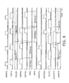
shift switch 21a forwards a final refresh signal from the last-stage shift register 19a(64) to the succeeding row block for use as a new refresh signal REFA00b in the first-stage shift register 19b(1) of thecell array 11b. This refresh signal is also directed to the RBLK latches 22a and 22b. In response to this, theRBLK latch 22a negates the row block selection signal RBLKEZa and stops feeding subordinate refresh pulses SREFPZa. Now that the external/internal address switching disable signal SNORSTXa is high, theRBLK latch 22a changes the state of address switching signals SREFCXa and SREFCZa to indicate that it is ready to accept data read/write requests. The refresh signal from theshift switch 21a further triggers the succeedingRBLK latch 22b to operate similarly to the above-describedRBLK latch 22a, so that itslocal cell array 11b will be refreshed. - Memory refresh is performed on an array-by-array basis. Referring now to the timing diagram of FIG. 8, we will look into how this switching is achieved. FIG. 8 shows signal waveforms in a transient period where the refresh control is transferred from one
cell array 11a to anothercell array 11b. - As FIG. 8 shows, the
RBLK latch 22a creates subordinate refresh pulses SREFPZa from main refresh pulses MREFPZ, while theshift command generator 23a produces a subordinate shift command signal SSFTXa from the main shift clock signal MSFTX. Theshift register 19a(63) captures the state of refresh signal REFA62a at the rising edge of the subordinate shift command signal SSFTXa and outputs it as a new refresh signal REFA63a at the falling edge of the same. - Simultaneously with the falling edge the refresh signal REFA63a, the
shift switch 21a outputs a refresh signal REFA00b, which is actually sent from the last-stage shift register 19a(64). This event deactivates the present row block selection signal RBLKEZa and activates the next row block selection signal RBLKEZb, instead. - The
shift command generator 23a produces one more pulse of subordinate shift command signal SSFTXa after the row block selection signal RBLKEZa is deactivated. This extra SSFTXa causes theshift register 19a(64) to remove the source of the refresh signal REFA00b. Theshift command generator 23b produces a subordinate shift command signal SSFTXb, thus allowing itslocal shift registers 19b(1) to 19b(64) (not all shown) to successively produce refresh signals REFA01b, REFA02b, and so on. - Shown on the third from the bottom row of FIG. 8 is a block reset signal BLTRZ, which is an active-high reset signal. As mentioned earlier in FIG. 6, the block reset signal BLTRZ cannot stop the generation of active-high address switching signal SREFCZ and its active-low counterpart SREFCX (which indicate that the
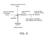
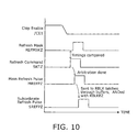
cell array 11a is in refresh mode) as long as the external/internal address switching disable signal SNORSTXa is asserted to low. - FIG. 9 shows a critical path that must be followed to initiate refresh operation. The round symbol represents an arbiter, and the bold arrows indicate the critical path. The arbiter is an integral part of the semiconductor memory device. Its function is to determine in what order to process given input signals, and to distribute those signals to their relevant processing circuits.
- The arbiter receives an active-low internal event status signal ICSX that indicates the presence of some ongoing internal event. Specifically, when ICSX is high, the arbiter permits other input signals to be serviced in the order of arrival. When ICSX is low, the arbiter suspends external commands and refresh request until the ongoing internal event is finished. The diagram of FIG. 9 assumes a high (inactive) state for this internal event status signal ICSX.
- Another input to the arbiter is an internal refresh command SRTZ, which represents a refresh request produced by a control circuit inside the device. Yet another input to the arbiter is a refresh mask signal REFMSKZ, which requests a halt of refresh operation. This refresh mask signal REFMSKZ is derived from an externally controlled chip enable signal /CE1. Specifically, the chip enable signal /CE1 indicates a read/write attempt from external circuitry, or a transition of the device itself to an output disable state.
- Once an internal refresh command SRTZ is recognized and allowed by the arbiter, the relevant control circuit in the semiconductor memory device generates main refresh pulses MREFPZ and distributes them to the RBLK latches 22 through a buffer circuit (not shown in FIG. 2). As described in FIG. 6, those main refresh pulses MREFPZ are then ANDed with a row block selection signal RBLKEZx, RBLKEZa, or the like for use as subordinate refresh pulse SREFPZa, SREFPZb, and the like.
- FIG. 10 is a timing diagram explaining a critical path that must be followed to initiate refresh operation. As seen, the process begins with assertion of chip enable signal /CE1, which activates refresh mask signal REFMSKZ. If there is an active internal refresh command SRTZ that has reached the arbiter earlier than the refresh mask signal REFMSKZ, the corresponding control circuit starts to generate main refresh pulses MREFPZ. The main refresh pulses MREFPZ are supplied to RBLK latch circuits 22 through buffers, and then ANDded with row block selection signals RBLKEZa, RBLKEZb, and so on. The resulting signals are sent out as subordinate refresh pulses SREFPZa, SREFPZb, or the like thus enabling refresh cycles to start.
- In the refresh process according to the present invention, the word lines are addressed successively by the shift registers 19. Conventional memory refresh mechanisms using an address counter spend time to fetch and decode address signals, wait for internal address to settle and activate a cell array, and activate timing signals. In contrast to this, the semiconductor memory device of the present invention needs no such time margins. While the above example is about memory access time from chip enable signal /CE1, the same advantage applies to address access time and other performance factors of memory devices.
- To summarize this section, the first embodiment of the invention provides RBLK latches 22 designed to send a subordinate shift command signal to a limited number of shift registers 19 that are currently generating main word line selection signals to refresh a cell array 11. This structure reduces the amount of electrical current consumed in driving subordinate shift command lines.
- This section will describe a second embodiment of the present invention. FIG. 11 is a schematic circuit diagram of a semiconductor memory device according to a second embodiment of the invention. The illustrated semiconductor memory device differs from the device of FIG. 2 in that it employs
buffers shift switches shift switch 21a controlsshift registers 19a(1) to 19a(64) such that their refresh signals REFA00a to REFA63a will circulate until all subordinate word lines of thecorresponding cell array 11a are refreshed. Theother shift switch 21x operates in the same way. The device of FIG. 11, on the other hand, is designed to advance the refresh process without waiting completion of all subordinate word lines of each cell array 11. That is, the refresh process scans all cell arrays 11 by successively activating main word lines, but not changing subordinate word line address. When one round of such scanning is finished, the next round starts with a different subordinate word line address. This is repeated until all subordinate word lines are refreshed. The following section will provide details of the second embodiment. Because the second embodiment (FIG. 11) shares many components with the first embodiment (FIG. 2), we will omit the explanation of such common components, while affixing the same reference numerals to them. - Referring to FIG. 11, the illustrated memory device has
buffers individual cell arrays buffer 41a transfers a refresh signal from the last-stage shift register 19a(64) to thesubsequent shift register 19b(1), as well as to thelocal RBLK latch 22a and precedingRBLK latch 22b. Likewise, thebuffer 41x receives a refresh signal from the last-stage shift register (not shown) of thecell array 11x. Thebuffer 41a transfers that refresh signal to its local RBLK latch (not shown) as well as to the first-stage shift register 19a (1) andRBLK latch 22a of the succeedingcell array 11a that is to be refreshed next. - The buffers 41 have no particular control inputs. This is unlike the device of the first embodiment (FIG. 2), in which the shift switches 21 are controlled by a shift flag signal FLAG. The buffers 41 in the second embodiment simply forward a refresh signal from the preceding shift register to the succeeding shift register immediately when it is produced. The refresh process therefore proceeds from one cell array to another without finishing all subordinate word lines at each cell. When the last cell array is reached, the process goes back to the first cell array and starts another round in a similar way, but selecting the next unfinished subordinate word line address.
- As can be seen from the above, the semiconductor memory device of the second embodiment is designed to repeat a simple circulation of a refresh signal through a large loop of shift registers and buffers, involving the entire set of cell arrays. Besides eliminating the wiring of shift flag signals FLAG, this architecture requires no feedback path of a refresh signal from a last-stage shift register to a first-stage shift register. The second embodiment is advantageous in terms of simplicity of refresh control circuit.
- The second embodiment also inherits the power saving feature from the first embodiment. That is, the RBLK latches 22 send a subordinate shift command signal to only a limited number of shift registers 19 that are currently active. This structure reduces the amount of electrical current consumed in driving subordinate shift command lines.
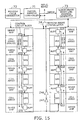
- This section describes a third embodiment of the present invention. FIG. 12 is a schematic circuit diagram of a semiconductor memory device according to a third embodiment of the invention. Unlike FIG. 2, FIG. 12 provides a wider perspective of a proposed semiconductor memory device. The illustrated memory device, however, is different from the device of FIG. 2 in that the cell arrays can be refreshed in partial refresh mode. Despite this difference, the two devices are similar in most part. More specifically, the cell arrays shown in FIG. 12 correspond to the cell arrays 11 explained in FIG. 2. Sense amplifiers in FIG. 12 correspond to the sense amplifiers 12 explained in FIG. 2. Shift register sets (SRS) in FIG. 12 correspond to the shift registers 19 explained in FIG. 2. Switches (SW) in FIG. 12 correspond to the shift switches 21 explained in FIG. 2, except that one
switch 53 is added a function that the shift switches 21 do not have. Control circuit blocks represented by the hatched rectangles in FIG. 12 include the RBLK latches 22, shift command generators 23, and control signal generators 24 explained in FIG. 2. RBLKEZ (indicated by the dotted arrows) in FIG. 12 are what we described in FIG. 2 as the row block selection signals RBLKEZx, RBLKEZa, and so on. RBLKRZ in FIG. 12 corresponds to the refresh signal path that extends from each shift switch 21 to its preceding RBLK latch 22. FLAG in FIG. 12 corresponds to the shift flag signal FLAG in FIG. 2. - In addition to the components named above, the semiconductor memory device of FIG. 12 has the following elements: a
partial refresh controller 51, arefresh cycle generator 52, a refresh array status latch 54, NOR gates Z41 and Z43, and inverters Z42, Z44, Z45, and Z46. - Cell arrays are blocks of memory cells arranged in matrix form, each block containing a predetermined number of rows (or word lines) . Those cell arrays are divided into two large groups. In partial refresh mode, the refresh process is interrupted in the middle of one group of cell arrays, and the control is transferred to the other group of cell arrays to continue the process. In the example of FIG. 12, cell arrays are divided into the left group and right group.
- The
partial refresh controller 51 accepts a partial refresh request from external circuitry, when the refresh process has returned to a predefined start point. Upon receipt of such a partial refresh request, thepartial refresh controller 51 produces a refresh area switching signal REFSW. In a partial refresh process, thepartial refresh controller 51 initiates individual refresh cycles at the intervals specified by therefresh cycle generator 52. When terminating the partial refresh mode, thepartial refresh controller 51 first expands the refresh area to the original entire memory area and then resets the refresh interval to normal interval. - The
refresh cycle generator 52 produces refresh timing signals for use in partial refresh operation. Usually therefresh cycle generator 52 specifies a prescribed interval for normal refresh mode, which covers the entire memory area. In partial refresh mode, therefresh cycle generator 52 varies the refresh interval according to the ratio of partial refresh area size to total memory size. - The
switch 53 functions as follows. When a final refresh signal appears at the output of the local shift register set, theswitch 53 normally forwards it to the succeeding shift register set. The exception is when a refresh area switching signal REFSW is given from thepartial refresh controller 51. In this case, theswitch 53 directs the refresh signal, not to the succeeding shift register set, but to the control circuit block of one cell array belonging to the other group (right group in FIG. 12). The NOR gate Z41 adjacent to theswitch 53 receives the refresh signal, whether theswitch 53 has directed it to the right cell array group or the succeeding shift register. The NOR gate Z41 sends this refresh signal through an inverter Z42 to the local control circuit block that serves the local shift register set. - The logic formed from a NOR gate Z43 and inverters Z44 to Z46 detects the transfer of a refresh signal from one group to the other (from the left group to the right group in FIG. 12) and notifies the refresh array status latch 54 of that event. The refresh array status latch 54 is also monitoring the other direction, i.e., from the right group to the left group. Monitoring those refresh signals transferred across the groups permits the refresh array status latch 54 to recognize which group of cell arrays is currently refreshed. Based on this knowledge, the refresh array status latch 54 asserts either one of two refresh area signals REFLZ or REFRZ. More specifically, REFLZ is set to low, and REFRZ is set to high, when a refresh signal has been transferred from the left group to the right group. REFLZ is set to high, and REFRZ is set to low, when a refresh signal has been transferred from the right group to the left group.
- FIG. 13 shows the entry to and exit from partial refresh mode and how refresh loops are created. The
cell array group 61 shown on the left represents the cell arrays located on the left-hand side of FIG. 12. The othercell array group 62 represents the cell arrays located on the right-hand side of FIG. 12. The symbols P1 to P6 and associated arrows shown in FIG. 13 indicate in what order thecell array groups cell array groups - FIG. 14 is a table showing the relationship between refresh areas shown in FIG. 13 and refresh intervals. The symbol "CE2" in this table means an input signal that allows external circuitry to direct the memory device to operate in partial refresh mode. The memory device performs normal refresh over the entire memory area when CE2 is high. Setting CE2 to low enables partial refresh. The AREA SIZE field of the table indicates the ratio of partial refresh area to the entire cell array area. For example, the AREA SIZE value "1/2" in the third row means that only half the total cell array area is refreshed in partial refresh mode.
- Enabling partial refresh mode with a high-to-low transition of CE2 alone would cause a problem. Suppose, for example, that CE2 is asserted when a refresh process is proceeding from point P2 to P5. Hastily changing the setup of refresh area and interval in response to this event would make it impossible for a refresh signal to be passed from point P3 to P4. For this reason, entry to partial refresh mode has to be deferred until the refresh signal returns to the initial point P1. As mentioned earlier, the refresh area signal REFLZ becomes high when a circulating refresh signal returns from the right group to the left group. That is, the high level of REFLZ suggests that the left group of cell arrays is ready to begin a partial refresh process from the initial point P1. The
partial refresh controller 51 then sets the refresh area to "x1/2" (half the entire area), and therefresh cycle generator 52 sets the refresh interval to "x2" (double the normal interval). - Another issue to consider is how to exit from partial refresh mode when the process is exactly at the branch point P2. The problem here is that this situation could bring about two parallel refresh processes, one from P2 to P5 and the other from P3 to P4. Yet another problematic case is where the exit from partial refresh mode occurs immediately before the branch point P2. In this case the memory cells located at point P3 would remain unrefreshed for as long as (14/8)T (T: minimum refresh time required for data retention), because the path P3-P4-P1-P2 takes time T and P2-P5-P6-P3 takes time 6/8T. To meet the requirement of minimum refresh rate, the refresh interval has to be reduced by the factor of 8/14. For this reason, the exit from partial refresh mode in the present invention is designed to start with changing the refresh interval to half the normal interval upon detection of a low-to-high transition of CE2. The refresh area signal REFLZ goes high when the remaining partial refresh area is finished, and this event causes the refresh area to revert to normal "x1" (i.e., the entire area). The next round thus refreshes all cell arrays at double speed, which ends with the second occurrence of high REFLZ. The refresh interval is reset to the normal interval at this point.
- The reason for halving the refresh interval before everything else is as follows. Suppose that the exit from partial refresh mode is triggered just after the point P1 is passed, immediately followed by a write operation to some address between P6 and P3. Since the path is not allowed to change to P1-P5-P6-P4 right away, the refresh process has to take the path of P1-P2-P3-P4 and then P1-P2-P5-P6-P3-P4. If refresh was done at the normal rate, the worst-case period for the above write address would amount to (5/4)T since the path P1-P2-P3-P4 takes time (1/2)T and P1-P5-P6-P3 takes time (3/4)T. To meet the requirement of minimum refresh rate, the refresh interval in partial refresh mode has to be set to 4/5 times the normal interval, resulting in an increased data retention current in standby mode. To avoid this undesirable current consumption, the refresh rate is temporarily raised when exiting from partial refresh mode.
- As seen, the example of FIG. 12 assumes such a memory chip structure where cell arrays are split into a left and right blocks, and the control circuit is designed to switch the refresh areas and intervals at a reference point where a refresh process jumps from the right to the left. The present invention, however, should not be limited to this particular configuration. For example, the reference point may be set to another appropriate point on the refresh address space.
- To summarize this section, the third embodiment of the present invention employs a
switch 53 at a point in the loop of shift registers to change the flow of refresh control signals. According to the state of a refresh area switching signal REFSW indicating the presence of a partial refresh request, theswitch 53 interrupts the ongoing refresh process in the middle of one of two major groups of cell arrays, so that the refresh process will continue in the other group of cell arrays. The present invention implements partial refresh mode in this way, which reduces the device's power consumption by limiting the number of cell arrays that need data refreshing. - This section will describe a fourth embodiment of the present invention. FIG. 15 is a schematic circuit diagram of a semiconductor memory device according to a fourth embodiment of the invention. Unlike FIG. 11, FIG. 15 provides a wider perspective of the proposed semiconductor memory device. The illustrated memory device, however, is different from the device of FIG. 11 in that the cell arrays can be refreshed in partial refresh mode. Despite this difference, the two devices are similar in most part. More specifically, the cell arrays shown in FIG. 15 correspond to the cell arrays 11 shown in FIG. 11. Sense amplifiers in FIG. 15 correspond to the sense amplifiers 12 shown in FIG. 11. Shift register sets (SRS) in FIG. 15 correspond to the shift registers 19 shown in FIG. 11. Buffers (BUFF) in FIG. 15 correspond to the buffers 41 explained in FIG. 11. Control circuit blocks represented by the hatched rectangles in FIG. 15 include the RBLK latches 22, shift command generators 23, and control signal generators 24 shown in FIG. 11. RBLKEZ (indicated by the dotted arrows) in FIG. 15 are the row block selection signals RBLKEZx, RBLKEZa, and the like shown in FIG. 11 RBLKRZ in FIG. 15 corresponds to the refresh signal path that extends from each shift switch 21 to its preceding RBLK latch 22.
- In addition to the components named above, the semiconductor memory device of FIG. 15 has the following elements: a
partial refresh controller 71, arefresh cycle generator 72, a refresharray status latch 74, and inverters Z47 and Z48. - Cell arrays are blocks of memory cells arranged in matrix form, each block containing a predetermined number of rows (or word lines). Those cell arrays are divided into two large groups. In the example of FIG. 15, they are divided into the left group and right group.
- The
partial refresh controller 71 accepts a partial refresh request from external circuitry when the refresh process has returned to a predefined start point. Upon acceptance of such a partial refresh request, thepartial refresh controller 71 sends a refresh area switching signal REFSW to the subordinate wordline address generator 73. In a partial refresh process, thepartial refresh controller 71 initiates individual refresh cycles at the intervals specified by therefresh cycle generator 72. - The
refresh cycle generator 72 produces refresh timing signals for use in partial refresh processes. Specifically, therefresh cycle generator 72 determines partial refresh intervals by dividing a specified interval of the entire memory refresh according to the ratio of partial refresh area size to total memory size. - The inverters Z47 to Z48 detects transfer of a refresh signal from one group to the other (from the left group to the right group in FIG. 15) and notifies the refresh
array status latch 74 of that event. - When the
partial refresh controller 71 has sent a refresh area switching signal REFSW indicating partial refresh mode, the subordinate wordline address generator 73 increments the subordinate word line address each time all main word lines are refreshed. The subordinate wordline address generator 73 actually skips some subordinate word lines. This is because the active range of subordinate word line address is defined in its upper digits including the most significant bit, depending on the size of a memory space that needs refresh. In other words, the subordinate wordline address generator 73 only varies this predefined upper portion of subordinate word line address, skipping some lowest bits. - The refresh
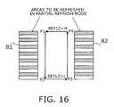
array status latch 74 monitors refresh signals transferred across the groups. By so doing, the refresh array status latch 54 can recognize which group of cell arrays is currently refreshed, and based on this knowledge, it asserts either one of two refresh area signals REFLZ or REFRZ. More specifically, REFLZ is set to low and REFRZ is set to high when a refresh signal has been transferred from the left group to the right group in FIG. 15. REFLZ is set to high and REFRZ is set to low when a refresh signal has been transferred from the right group to the left group. - FIG. 16 shows the entry to and exit from partial refresh mode and explains how refresh loops are created. The
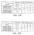
cell array group 81 shown on the left represents the cell arrays located on the left-hand side of FIG. 15. The othercell array group 82 represents the cell arrays located on the right-hand side of FIG. 12. The symbols P1 to P4 and associated arrows shown in FIG. 16 indicate in what order thecell array groups cell array groups - FIG. 17A gives a table showing the relationship between the refresh areas shown in FIG. 16 and refresh intervals. The symbol "CE2" in this table denotes an input signal that allows external circuitry to direct the memory device to operate in partial refresh mode. The memory device performs normal refresh over the entire memory area when CE2 is high. Setting CE2 to low enables partial refresh. The AREA SIZE field of the table indicates the ratio of partial refresh area to the entire cell array area. For example, the AREA SIZE value "1/2" shown in the third row of the table means that only half the total cell array area is refreshed in partial refresh mode.
- The table of FIG. 17A represents the following scenario. When CE2 is asserted to low, the
partial refresh controller 71 waits until the refresh area signal REFLZ becomes high. Upon detection of this REFLZ, thepartial refresh controller 71 halves the refresh area, and therefresh cycle generator 72 doubles the refresh interval. As FIG. 16 shows, the refresh process always follows the same path P1-P2-P3-P4. The refresh intervals can be doubled simply because the refresh area is reduced to half. Afterwards, CE2 returns to high, and the memory device exits from partial refresh mode by resetting the refresh area to "x1" (i.e., entire area) and refresh interval to "x1" (i. e., normal interval). - FIG. 17B is a table showing an alternative control method that can be applied to the fourth embodiment. When CE2 is asserted to low, the
partial refresh controller 71 enters to partial refresh mode immediately. In partial refresh mode, thepartial refresh controller 71 keeps scanning address at normal refresh intervals, and if it encounters an address that is out of the predetermined partial refresh area, thecontroller 71 simply skips the refresh cycle of that address by masking a refresh start command. In this way the refresh area is substantively reduced. When CE2 returns to high, the memory device exits from partial refresh mode by resetting the refresh area to "x1" (i.e., entire area). - As can be seen from the above, the architecture of FIG. 15 requires no special steps when changing the refresh interval to exit from partial refresh mode. This is because the refresh process follows the same path P1-P2-P3-P4, whether it is in normal refresh mode or partial refresh mode. That is, the semiconductor memory device of FIG. 15 is advantageous over the device of FIG. 12 in terms of the simplicity of control in exiting from partial refresh mode.
- The fourth embodiment of the present invention accomplishes partial refresh by repeating a refresh cycle for entire cell arrays while skipping some bits of subordinate word line address. This refresh mode limits the number of subordinate word lines to be refreshed, thus reducing the device's power consumption.
- In conclusion, the present invention provides a semiconductor memory device with a shift register-based refresh address generation function. Shift registers provide each cell array with word line selection signals for use in refresh operation, under the control of dedicated shift register controllers. The shift register controllers are designed to activate a minimum number of shift registers that need to operate. This feature of the present invention reduces the amount of electrical current consumed in driving shift register control signals.
- The foregoing is considered as illustrative only of the principles of the present invention. Further, since numerous modifications, changes will readily occur to those skilled in the art, it is not desired to limit the invention to the exact construction, applications shown, described,, accordingly, all suitable modifications, equivalents may be regarded as falling within the scope of the invention in the appended claims, their equivalents.
Claims (12)
- A semiconductor memory device with a function of refreshing stored data, comprising:a plurality of cell arrays, each composed of a predetermined number of rows of memory cells;a plurality of sets of shift registers, an nth set of shift registers successively activating word line selection signals according to a given control signal, so as to refresh corresponding word lines of an nth cell array; anda plurality of shift register controllers, an nth shift register controller providing the control signal to the nth set of shift registers when the nth cell array is being refreshed, the nth shift register controller forwarding the control signal to an (n+1) th set of shift registers when said refresh of the nth cell array is finished.
- The semiconductor memory device according to claim 1, wherein the control signal that the nth shift register controller forwards to the (n+1) th set of shift registers is the word line selection signal used to refresh the last word line of the nth cell array.
- The semiconductor memory device according to claim 1, wherein:the word lines are hierarchically composed of main word lines and subordinate word lines; andthe nth shift register controller forwards the control signal to the (n+1)th set of shift registers when refresh of all the subordinate word lines of the nth cell array is finished.
- The semiconductor memory device according to claim 1, wherein:the word lines are hierarchically composed of main word lines and subordinate word lines; andsubordinate word line address specifying which subordinate word line to refresh is advanced each time the main word lines of the nth cell array are all refreshed.
- The semiconductor memory device according to claim 1, wherein:the plurality of cell arrays are divided into a plurality of groups of cell arrays; andthe semiconductor memory device further comprises a partial refresh controller that controls refresh of a limited refresh area of the plurality of groups in partial refresh mode.
- The semiconductor memory device according to claim 5, wherein:one of the plurality of cell arrays is designated as a refresh start point; andthe partial refresh controller accepts a partial refresh request only when a refresh process has circulated among the cell arrays and returned to the refresh start point.
- The semiconductor memory device according to claim 5, wherein, in the partial refresh mode, the partial refresh controller sets a refresh interval in inverse proportion to a ratio of the limited refresh area relative to an entire area of the cell arrays.
- The semiconductor memory device according to claim 7, wherein the partial refresh controller exits from the partial refresh mode by expanding the refresh interval to the entire area of the cell arrays and then resetting the refresh interval to a normal interval.
- The semiconductor memory device according to claim 4, wherein not all the subordinate word lines are selected in partial refresh mode.
- The semiconductor memory device according to claim 1, wherein address selection of the cell arrays is locked by an external/internal address switching disable signal during a refresh process so that the cell arrays use internally generated address.
- The semiconductor memory device according to claim 1, further comprising a plurality of redundancy circuits, one for each of the word lines, to repair a defect in the memory cells.
- The semiconductor memory device according to claim 1, wherein data in said cell arrays are read out through shared sense amplifiers.
Applications Claiming Priority (2)
| Application Number | Priority Date | Filing Date | Title |
|---|---|---|---|
| JP2003071660A JP4381013B2 (en) | 2003-03-17 | 2003-03-17 | Semiconductor memory device |
| JP2003071660 | 2003-03-17 |
Publications (3)
| Publication Number | Publication Date |
|---|---|
| EP1460638A2 true EP1460638A2 (en) | 2004-09-22 |
| EP1460638A3 EP1460638A3 (en) | 2005-04-27 |
| EP1460638B1 EP1460638B1 (en) | 2007-01-10 |
Family
ID=32821283
Family Applications (1)
| Application Number | Title | Priority Date | Filing Date |
|---|---|---|---|
| EP04005805A Expired - Fee Related EP1460638B1 (en) | 2003-03-17 | 2004-03-11 | Semiconductor memory device with shift register-based refresh address generation circuit |
Country Status (5)
| Country | Link |
|---|---|
| US (2) | US7145825B2 (en) |
| EP (1) | EP1460638B1 (en) |
| JP (1) | JP4381013B2 (en) |
| CN (1) | CN1530962B (en) |
| DE (1) | DE602004004182T2 (en) |
Cited By (1)
| Publication number | Priority date | Publication date | Assignee | Title |
|---|---|---|---|---|
| WO2017205378A1 (en) | 2016-05-25 | 2017-11-30 | Advanced Micro Devices, Inc. | Fine granularity refresh |
Families Citing this family (57)
| Publication number | Priority date | Publication date | Assignee | Title |
|---|---|---|---|---|
| WO2004095466A1 (en) * | 2003-04-23 | 2004-11-04 | Fujitsu Limited | Semiconductor memory |
| TWI269166B (en) * | 2005-04-22 | 2006-12-21 | Via Tech Inc | Automatic memory-updating method |
| US8327104B2 (en) | 2006-07-31 | 2012-12-04 | Google Inc. | Adjusting the timing of signals associated with a memory system |
| US7643430B2 (en) * | 2005-11-30 | 2010-01-05 | Cisco Technology, Inc. | Methods and apparatus for determining reverse path delay |
| KR101096255B1 (en) * | 2009-06-26 | 2011-12-22 | 주식회사 하이닉스반도체 | Counter control signal generation circuit and refresh circuit |
| US8045401B2 (en) * | 2009-09-18 | 2011-10-25 | Arm Limited | Supporting scan functions within memories |
| US8310893B2 (en) * | 2009-12-16 | 2012-11-13 | Micron Technology, Inc. | Techniques for reducing impact of array disturbs in a semiconductor memory device |
| US8774010B2 (en) | 2010-11-02 | 2014-07-08 | Cisco Technology, Inc. | System and method for providing proactive fault monitoring in a network environment |
| US8559341B2 (en) | 2010-11-08 | 2013-10-15 | Cisco Technology, Inc. | System and method for providing a loop free topology in a network environment |
| US8982733B2 (en) | 2011-03-04 | 2015-03-17 | Cisco Technology, Inc. | System and method for managing topology changes in a network environment |
| US8670326B1 (en) | 2011-03-31 | 2014-03-11 | Cisco Technology, Inc. | System and method for probing multiple paths in a network environment |
| US8724517B1 (en) | 2011-06-02 | 2014-05-13 | Cisco Technology, Inc. | System and method for managing network traffic disruption |
| US8830875B1 (en) | 2011-06-15 | 2014-09-09 | Cisco Technology, Inc. | System and method for providing a loop free topology in a network environment |
| KR20130117424A (en) * | 2012-04-17 | 2013-10-28 | 삼성전자주식회사 | Refresh circuit in semiconductor memory device |
| KR20130129786A (en) * | 2012-05-21 | 2013-11-29 | 에스케이하이닉스 주식회사 | Method for refresh and semiconductor memory device using the same |
| US9450846B1 (en) | 2012-10-17 | 2016-09-20 | Cisco Technology, Inc. | System and method for tracking packets in a network environment |
| US9324398B2 (en) * | 2013-02-04 | 2016-04-26 | Micron Technology, Inc. | Apparatuses and methods for targeted refreshing of memory |
| CN110069420A (en) * | 2013-04-02 | 2019-07-30 | 太阳诱电株式会社 | Semiconductor device |
| US9047978B2 (en) | 2013-08-26 | 2015-06-02 | Micron Technology, Inc. | Apparatuses and methods for selective row refreshes |
| JP2015219938A (en) | 2014-05-21 | 2015-12-07 | マイクロン テクノロジー, インク. | Semiconductor device |
| JP2017182854A (en) | 2016-03-31 | 2017-10-05 | マイクロン テクノロジー, インク. | Semiconductor device |
| US10490251B2 (en) | 2017-01-30 | 2019-11-26 | Micron Technology, Inc. | Apparatuses and methods for distributing row hammer refresh events across a memory device |
| US10192608B2 (en) * | 2017-05-23 | 2019-01-29 | Micron Technology, Inc. | Apparatuses and methods for detection refresh starvation of a memory |
| US10580475B2 (en) | 2018-01-22 | 2020-03-03 | Micron Technology, Inc. | Apparatuses and methods for calculating row hammer refresh addresses in a semiconductor device |
| US11017833B2 (en) | 2018-05-24 | 2021-05-25 | Micron Technology, Inc. | Apparatuses and methods for pure-time, self adopt sampling for row hammer refresh sampling |
| US11152050B2 (en) | 2018-06-19 | 2021-10-19 | Micron Technology, Inc. | Apparatuses and methods for multiple row hammer refresh address sequences |
| US10685696B2 (en) | 2018-10-31 | 2020-06-16 | Micron Technology, Inc. | Apparatuses and methods for access based refresh timing |
| WO2020117686A1 (en) | 2018-12-03 | 2020-06-11 | Micron Technology, Inc. | Semiconductor device performing row hammer refresh operation |
| CN117198356A (en) | 2018-12-21 | 2023-12-08 | 美光科技公司 | Apparatus and method for timing interleaving for targeted refresh operations |
| US10770127B2 (en) | 2019-02-06 | 2020-09-08 | Micron Technology, Inc. | Apparatuses and methods for managing row access counts |
| US11043254B2 (en) | 2019-03-19 | 2021-06-22 | Micron Technology, Inc. | Semiconductor device having cam that stores address signals |
| US11227649B2 (en) | 2019-04-04 | 2022-01-18 | Micron Technology, Inc. | Apparatuses and methods for staggered timing of targeted refresh operations |
| US11264096B2 (en) | 2019-05-14 | 2022-03-01 | Micron Technology, Inc. | Apparatuses, systems, and methods for a content addressable memory cell with latch and comparator circuits |
| US11158364B2 (en) | 2019-05-31 | 2021-10-26 | Micron Technology, Inc. | Apparatuses and methods for tracking victim rows |
| US11069393B2 (en) | 2019-06-04 | 2021-07-20 | Micron Technology, Inc. | Apparatuses and methods for controlling steal rates |
| US11158373B2 (en) | 2019-06-11 | 2021-10-26 | Micron Technology, Inc. | Apparatuses, systems, and methods for determining extremum numerical values |
| US11139015B2 (en) | 2019-07-01 | 2021-10-05 | Micron Technology, Inc. | Apparatuses and methods for monitoring word line accesses |
| US10832792B1 (en) | 2019-07-01 | 2020-11-10 | Micron Technology, Inc. | Apparatuses and methods for adjusting victim data |
| US11386946B2 (en) | 2019-07-16 | 2022-07-12 | Micron Technology, Inc. | Apparatuses and methods for tracking row accesses |
| US10943636B1 (en) | 2019-08-20 | 2021-03-09 | Micron Technology, Inc. | Apparatuses and methods for analog row access tracking |
| US10964378B2 (en) | 2019-08-22 | 2021-03-30 | Micron Technology, Inc. | Apparatus and method including analog accumulator for determining row access rate and target row address used for refresh operation |
| US11200942B2 (en) | 2019-08-23 | 2021-12-14 | Micron Technology, Inc. | Apparatuses and methods for lossy row access counting |
| US11302374B2 (en) | 2019-08-23 | 2022-04-12 | Micron Technology, Inc. | Apparatuses and methods for dynamic refresh allocation |
| US11302377B2 (en) | 2019-10-16 | 2022-04-12 | Micron Technology, Inc. | Apparatuses and methods for dynamic targeted refresh steals |
| US11309010B2 (en) | 2020-08-14 | 2022-04-19 | Micron Technology, Inc. | Apparatuses, systems, and methods for memory directed access pause |
| US11348631B2 (en) | 2020-08-19 | 2022-05-31 | Micron Technology, Inc. | Apparatuses, systems, and methods for identifying victim rows in a memory device which cannot be simultaneously refreshed |
| US11380382B2 (en) | 2020-08-19 | 2022-07-05 | Micron Technology, Inc. | Refresh logic circuit layout having aggressor detector circuit sampling circuit and row hammer refresh control circuit |
| US11222682B1 (en) | 2020-08-31 | 2022-01-11 | Micron Technology, Inc. | Apparatuses and methods for providing refresh addresses |
| US11557331B2 (en) | 2020-09-23 | 2023-01-17 | Micron Technology, Inc. | Apparatuses and methods for controlling refresh operations |
| US11222686B1 (en) | 2020-11-12 | 2022-01-11 | Micron Technology, Inc. | Apparatuses and methods for controlling refresh timing |
| US11462291B2 (en) | 2020-11-23 | 2022-10-04 | Micron Technology, Inc. | Apparatuses and methods for tracking word line accesses |
| US11264079B1 (en) | 2020-12-18 | 2022-03-01 | Micron Technology, Inc. | Apparatuses and methods for row hammer based cache lockdown |
| US11482275B2 (en) | 2021-01-20 | 2022-10-25 | Micron Technology, Inc. | Apparatuses and methods for dynamically allocated aggressor detection |
| US11600314B2 (en) | 2021-03-15 | 2023-03-07 | Micron Technology, Inc. | Apparatuses and methods for sketch circuits for refresh binning |
| US11664063B2 (en) | 2021-08-12 | 2023-05-30 | Micron Technology, Inc. | Apparatuses and methods for countering memory attacks |
| US11790974B2 (en) | 2021-11-17 | 2023-10-17 | Micron Technology, Inc. | Apparatuses and methods for refresh compliance |
| US11688451B2 (en) | 2021-11-29 | 2023-06-27 | Micron Technology, Inc. | Apparatuses, systems, and methods for main sketch and slim sketch circuit for row address tracking |
Citations (1)
| Publication number | Priority date | Publication date | Assignee | Title |
|---|---|---|---|---|
| EP0188769A2 (en) * | 1984-12-25 | 1986-07-30 | Fujitsu Limited | Dynamic type semiconductor memory device |
Family Cites Families (4)
| Publication number | Priority date | Publication date | Assignee | Title |
|---|---|---|---|---|
| JPH09161478A (en) * | 1995-12-12 | 1997-06-20 | Mitsubishi Electric Corp | Semiconductor memory |
| JP2000311487A (en) | 1999-04-27 | 2000-11-07 | Mitsubishi Electric Corp | Semiconductor memory |
| US6633952B2 (en) * | 2000-10-03 | 2003-10-14 | Broadcom Corporation | Programmable refresh scheduler for embedded DRAMs |
| JP3737437B2 (en) * | 2001-02-01 | 2006-01-18 | Necエレクトロニクス株式会社 | Semiconductor memory and entry method of operation mode thereof |
-
2003
- 2003-03-17 JP JP2003071660A patent/JP4381013B2/en not_active Expired - Fee Related
-
2004
- 2004-03-11 EP EP04005805A patent/EP1460638B1/en not_active Expired - Fee Related
- 2004-03-11 DE DE602004004182T patent/DE602004004182T2/en not_active Expired - Lifetime
- 2004-03-16 US US10/800,831 patent/US7145825B2/en not_active Expired - Fee Related
- 2004-03-17 CN CN2004100294355A patent/CN1530962B/en not_active Expired - Fee Related
-
2006
- 2006-07-14 US US11/486,002 patent/US7286434B2/en not_active Expired - Fee Related
Patent Citations (1)
| Publication number | Priority date | Publication date | Assignee | Title |
|---|---|---|---|---|
| EP0188769A2 (en) * | 1984-12-25 | 1986-07-30 | Fujitsu Limited | Dynamic type semiconductor memory device |
Cited By (2)
| Publication number | Priority date | Publication date | Assignee | Title |
|---|---|---|---|---|
| WO2017205378A1 (en) | 2016-05-25 | 2017-11-30 | Advanced Micro Devices, Inc. | Fine granularity refresh |
| EP3433860A4 (en) * | 2016-05-25 | 2019-11-20 | Advanced Micro Devices, Inc. | Fine granularity refresh |
Also Published As
| Publication number | Publication date |
|---|---|
| DE602004004182T2 (en) | 2007-10-25 |
| US7286434B2 (en) | 2007-10-23 |
| EP1460638A3 (en) | 2005-04-27 |
| US20060256638A1 (en) | 2006-11-16 |
| CN1530962A (en) | 2004-09-22 |
| EP1460638B1 (en) | 2007-01-10 |
| JP4381013B2 (en) | 2009-12-09 |
| JP2004280957A (en) | 2004-10-07 |
| US7145825B2 (en) | 2006-12-05 |
| US20040184323A1 (en) | 2004-09-23 |
| DE602004004182D1 (en) | 2007-02-22 |
| CN1530962B (en) | 2010-06-02 |
Similar Documents
| Publication | Publication Date | Title |
|---|---|---|
| EP1460638B1 (en) | Semiconductor memory device with shift register-based refresh address generation circuit | |
| DE60005645T2 (en) | Semiconductor memory device with reduced power consumption in data hold mode | |
| EP1255254B1 (en) | Word line driver for a semiconductor memory device | |
| US20020031030A1 (en) | Dram Capable Of Selectively Performing Self-Refresh Operation For Memory Bank | |
| US5521527A (en) | Semiconductor integrated circuits with power reduction mechanism | |
| US20060018174A1 (en) | Semiconductor memory device performing auto refresh in the self refresh mode | |
| US7102936B2 (en) | Internal voltage generating circuit for periphery, semiconductor memory device having the circuit and method thereof | |
| US6504783B2 (en) | Semiconductor device having early operation high voltage generator and high voltage supplying method therefor | |
| US5335201A (en) | Method for providing synchronous refresh cycles in self-refreshing interruptable DRAMs | |
| US20150023121A1 (en) | Memory refresh methods, memory section control circuits, and apparatuses | |
| CN1034373C (en) | Boosting circuit device capable of pre-pumping and semiconducotr memory device | |
| EP0782141B1 (en) | Voltage pumping circuit for semiconductor memory device | |
| KR100203724B1 (en) | Memory device with hierarchical boosted power line sheme | |
| US20040184336A1 (en) | Reducing digit equilibrate current during self-refresh mode | |
| WO1994022222A1 (en) | Dynamic control of configurable logic | |
| CN112133346B (en) | Apparatus and method for controlling word line discharge | |
| JPH04321252A (en) | Dynamic random access memory device | |
| JPH08190789A (en) | Dynamic semiconductor storage | |
| US7426151B2 (en) | Device and method for performing a partial array refresh operation | |
| JPH08167291A (en) | Semiconductor memory device | |
| US5229969A (en) | Method for synchronizing refresh cycles in self-refreshing DRAMs having timing circuit shutdown | |
| EP0811980A2 (en) | Low voltage bootstrapping circuit | |
| US6191995B1 (en) | Sharing signal lines in a memory device | |
| EP0337172B1 (en) | Static random access memory device with a power dissipation reduction function | |
| US5802008A (en) | Word line driver in semiconductor memory device using a main decoder and a plurality of middle and sub-decoders |
Legal Events
| Date | Code | Title | Description |
|---|---|---|---|
| PUAI | Public reference made under article 153(3) epc to a published international application that has entered the european phase |
Free format text: ORIGINAL CODE: 0009012 |
|
| AK | Designated contracting states |
Kind code of ref document: A2 Designated state(s): AT BE BG CH CY CZ DE DK EE ES FI FR GB GR HU IE IT LI LU MC NL PL PT RO SE SI SK TR |
|
| AX | Request for extension of the european patent |
Extension state: AL LT LV MK |
|
| PUAL | Search report despatched |
Free format text: ORIGINAL CODE: 0009013 |
|
| AK | Designated contracting states |
Kind code of ref document: A3 Designated state(s): AT BE BG CH CY CZ DE DK EE ES FI FR GB GR HU IE IT LI LU MC NL PL PT RO SE SI SK TR |
|
| AX | Request for extension of the european patent |
Extension state: AL LT LV MK |
|
| 17P | Request for examination filed |
Effective date: 20050412 |
|
| 17Q | First examination report despatched |
Effective date: 20050603 |
|
| AKX | Designation fees paid |
Designated state(s): DE FR IT |
|
| GRAP | Despatch of communication of intention to grant a patent |
Free format text: ORIGINAL CODE: EPIDOSNIGR1 |
|
| GRAS | Grant fee paid |
Free format text: ORIGINAL CODE: EPIDOSNIGR3 |
|
| GRAA | (expected) grant |
Free format text: ORIGINAL CODE: 0009210 |
|
| AK | Designated contracting states |
Kind code of ref document: B1 Designated state(s): DE FR IT |
|
| REF | Corresponds to: |
Ref document number: 602004004182 Country of ref document: DE Date of ref document: 20070222 Kind code of ref document: P |
|
| ET | Fr: translation filed | ||
| PLBE | No opposition filed within time limit |
Free format text: ORIGINAL CODE: 0009261 |
|
| STAA | Information on the status of an ep patent application or granted ep patent |
Free format text: STATUS: NO OPPOSITION FILED WITHIN TIME LIMIT |
|
| 26N | No opposition filed |
Effective date: 20071011 |
|
| REG | Reference to a national code |
Ref country code: FR Ref legal event code: TP |
|
| PGFP | Annual fee paid to national office [announced via postgrant information from national office to epo] |
Ref country code: IT Payment date: 20090321 Year of fee payment: 6 |
|
| PGFP | Annual fee paid to national office [announced via postgrant information from national office to epo] |
Ref country code: FR Payment date: 20090316 Year of fee payment: 6 |
|
| REG | Reference to a national code |
Ref country code: FR Ref legal event code: ST Effective date: 20101130 |
|
| PG25 | Lapsed in a contracting state [announced via postgrant information from national office to epo] |
Ref country code: FR Free format text: LAPSE BECAUSE OF NON-PAYMENT OF DUE FEES Effective date: 20100331 |
|
| PG25 | Lapsed in a contracting state [announced via postgrant information from national office to epo] |
Ref country code: IT Free format text: LAPSE BECAUSE OF NON-PAYMENT OF DUE FEES Effective date: 20100311 |
|
| REG | Reference to a national code |
Ref country code: DE Ref legal event code: R082 Ref document number: 602004004182 Country of ref document: DE Representative=s name: REICHERT & LINDNER PARTNERSCHAFT PATENTANWAELT, DE |
|
| REG | Reference to a national code |
Ref country code: DE Ref legal event code: R081 Ref document number: 602004004182 Country of ref document: DE Owner name: SOCIONEXT INC., YOKOHAMA-SHI, JP Free format text: FORMER OWNER: FUJITSU SEMICONDUCTOR LTD., YOKOHAMA, KANAGAWA, JP Effective date: 20150512 Ref country code: DE Ref legal event code: R082 Ref document number: 602004004182 Country of ref document: DE Representative=s name: REICHERT & LINDNER PARTNERSCHAFT PATENTANWAELT, DE Effective date: 20150512 |
|
| PGFP | Annual fee paid to national office [announced via postgrant information from national office to epo] |
Ref country code: DE Payment date: 20190321 Year of fee payment: 16 |
|
| REG | Reference to a national code |
Ref country code: DE Ref legal event code: R119 Ref document number: 602004004182 Country of ref document: DE |
|
| PG25 | Lapsed in a contracting state [announced via postgrant information from national office to epo] |
Ref country code: DE Free format text: LAPSE BECAUSE OF NON-PAYMENT OF DUE FEES Effective date: 20201001 |