EP1460607A1 - Production method for plane-type display unit - Google Patents
Production method for plane-type display unit Download PDFInfo
- Publication number
- EP1460607A1 EP1460607A1 EP02793384A EP02793384A EP1460607A1 EP 1460607 A1 EP1460607 A1 EP 1460607A1 EP 02793384 A EP02793384 A EP 02793384A EP 02793384 A EP02793384 A EP 02793384A EP 1460607 A1 EP1460607 A1 EP 1460607A1
- Authority
- EP
- European Patent Office
- Prior art keywords
- region
- flat
- regions
- manufacturing
- display apparatuses
- Prior art date
- Legal status (The legal status is an assumption and is not a legal conclusion. Google has not performed a legal analysis and makes no representation as to the accuracy of the status listed.)
- Withdrawn
Links
Images




Classifications
-
- H—ELECTRICITY
- H01—ELECTRIC ELEMENTS
- H01J—ELECTRIC DISCHARGE TUBES OR DISCHARGE LAMPS
- H01J9/00—Apparatus or processes specially adapted for the manufacture, installation, removal, maintenance of electric discharge tubes, discharge lamps, or parts thereof; Recovery of material from discharge tubes or lamps
- H01J9/24—Manufacture or joining of vessels, leading-in conductors or bases
- H01J9/241—Manufacture or joining of vessels, leading-in conductors or bases the vessel being for a flat panel display
-
- G—PHYSICS
- G02—OPTICS
- G02F—OPTICAL DEVICES OR ARRANGEMENTS FOR THE CONTROL OF LIGHT BY MODIFICATION OF THE OPTICAL PROPERTIES OF THE MEDIA OF THE ELEMENTS INVOLVED THEREIN; NON-LINEAR OPTICS; FREQUENCY-CHANGING OF LIGHT; OPTICAL LOGIC ELEMENTS; OPTICAL ANALOGUE/DIGITAL CONVERTERS
- G02F1/00—Devices or arrangements for the control of the intensity, colour, phase, polarisation or direction of light arriving from an independent light source, e.g. switching, gating or modulating; Non-linear optics
- G02F1/01—Devices or arrangements for the control of the intensity, colour, phase, polarisation or direction of light arriving from an independent light source, e.g. switching, gating or modulating; Non-linear optics for the control of the intensity, phase, polarisation or colour
- G02F1/13—Devices or arrangements for the control of the intensity, colour, phase, polarisation or direction of light arriving from an independent light source, e.g. switching, gating or modulating; Non-linear optics for the control of the intensity, phase, polarisation or colour based on liquid crystals, e.g. single liquid crystal display cells
-
- G—PHYSICS
- G02—OPTICS
- G02F—OPTICAL DEVICES OR ARRANGEMENTS FOR THE CONTROL OF LIGHT BY MODIFICATION OF THE OPTICAL PROPERTIES OF THE MEDIA OF THE ELEMENTS INVOLVED THEREIN; NON-LINEAR OPTICS; FREQUENCY-CHANGING OF LIGHT; OPTICAL LOGIC ELEMENTS; OPTICAL ANALOGUE/DIGITAL CONVERTERS
- G02F1/00—Devices or arrangements for the control of the intensity, colour, phase, polarisation or direction of light arriving from an independent light source, e.g. switching, gating or modulating; Non-linear optics
- G02F1/01—Devices or arrangements for the control of the intensity, colour, phase, polarisation or direction of light arriving from an independent light source, e.g. switching, gating or modulating; Non-linear optics for the control of the intensity, phase, polarisation or colour
- G02F1/13—Devices or arrangements for the control of the intensity, colour, phase, polarisation or direction of light arriving from an independent light source, e.g. switching, gating or modulating; Non-linear optics for the control of the intensity, phase, polarisation or colour based on liquid crystals, e.g. single liquid crystal display cells
- G02F1/133—Constructional arrangements; Operation of liquid crystal cells; Circuit arrangements
- G02F1/1333—Constructional arrangements; Manufacturing methods
-
- G—PHYSICS
- G02—OPTICS
- G02F—OPTICAL DEVICES OR ARRANGEMENTS FOR THE CONTROL OF LIGHT BY MODIFICATION OF THE OPTICAL PROPERTIES OF THE MEDIA OF THE ELEMENTS INVOLVED THEREIN; NON-LINEAR OPTICS; FREQUENCY-CHANGING OF LIGHT; OPTICAL LOGIC ELEMENTS; OPTICAL ANALOGUE/DIGITAL CONVERTERS
- G02F1/00—Devices or arrangements for the control of the intensity, colour, phase, polarisation or direction of light arriving from an independent light source, e.g. switching, gating or modulating; Non-linear optics
- G02F1/01—Devices or arrangements for the control of the intensity, colour, phase, polarisation or direction of light arriving from an independent light source, e.g. switching, gating or modulating; Non-linear optics for the control of the intensity, phase, polarisation or colour
- G02F1/13—Devices or arrangements for the control of the intensity, colour, phase, polarisation or direction of light arriving from an independent light source, e.g. switching, gating or modulating; Non-linear optics for the control of the intensity, phase, polarisation or colour based on liquid crystals, e.g. single liquid crystal display cells
- G02F1/133—Constructional arrangements; Operation of liquid crystal cells; Circuit arrangements
- G02F1/1333—Constructional arrangements; Manufacturing methods
- G02F1/133351—Manufacturing of individual cells out of a plurality of cells, e.g. by dicing
-
- H—ELECTRICITY
- H01—ELECTRIC ELEMENTS
- H01J—ELECTRIC DISCHARGE TUBES OR DISCHARGE LAMPS
- H01J9/00—Apparatus or processes specially adapted for the manufacture, installation, removal, maintenance of electric discharge tubes, discharge lamps, or parts thereof; Recovery of material from discharge tubes or lamps
- H01J9/24—Manufacture or joining of vessels, leading-in conductors or bases
-
- G—PHYSICS
- G02—OPTICS
- G02F—OPTICAL DEVICES OR ARRANGEMENTS FOR THE CONTROL OF LIGHT BY MODIFICATION OF THE OPTICAL PROPERTIES OF THE MEDIA OF THE ELEMENTS INVOLVED THEREIN; NON-LINEAR OPTICS; FREQUENCY-CHANGING OF LIGHT; OPTICAL LOGIC ELEMENTS; OPTICAL ANALOGUE/DIGITAL CONVERTERS
- G02F1/00—Devices or arrangements for the control of the intensity, colour, phase, polarisation or direction of light arriving from an independent light source, e.g. switching, gating or modulating; Non-linear optics
- G02F1/01—Devices or arrangements for the control of the intensity, colour, phase, polarisation or direction of light arriving from an independent light source, e.g. switching, gating or modulating; Non-linear optics for the control of the intensity, phase, polarisation or colour
- G02F1/13—Devices or arrangements for the control of the intensity, colour, phase, polarisation or direction of light arriving from an independent light source, e.g. switching, gating or modulating; Non-linear optics for the control of the intensity, phase, polarisation or colour based on liquid crystals, e.g. single liquid crystal display cells
- G02F1/133—Constructional arrangements; Operation of liquid crystal cells; Circuit arrangements
- G02F1/1333—Constructional arrangements; Manufacturing methods
- G02F1/133354—Arrangements for aligning or assembling substrates
-
- G—PHYSICS
- G02—OPTICS
- G02F—OPTICAL DEVICES OR ARRANGEMENTS FOR THE CONTROL OF LIGHT BY MODIFICATION OF THE OPTICAL PROPERTIES OF THE MEDIA OF THE ELEMENTS INVOLVED THEREIN; NON-LINEAR OPTICS; FREQUENCY-CHANGING OF LIGHT; OPTICAL LOGIC ELEMENTS; OPTICAL ANALOGUE/DIGITAL CONVERTERS
- G02F1/00—Devices or arrangements for the control of the intensity, colour, phase, polarisation or direction of light arriving from an independent light source, e.g. switching, gating or modulating; Non-linear optics
- G02F1/01—Devices or arrangements for the control of the intensity, colour, phase, polarisation or direction of light arriving from an independent light source, e.g. switching, gating or modulating; Non-linear optics for the control of the intensity, phase, polarisation or colour
- G02F1/13—Devices or arrangements for the control of the intensity, colour, phase, polarisation or direction of light arriving from an independent light source, e.g. switching, gating or modulating; Non-linear optics for the control of the intensity, phase, polarisation or colour based on liquid crystals, e.g. single liquid crystal display cells
- G02F1/133—Constructional arrangements; Operation of liquid crystal cells; Circuit arrangements
- G02F1/1333—Constructional arrangements; Manufacturing methods
- G02F1/1345—Conductors connecting electrodes to cell terminals
- G02F1/13452—Conductors connecting driver circuitry and terminals of panels
Definitions
- This invention relates to a manufacturing method for flat display apparatuses.
- LCD liquid crystal display
- PDP plasma display panel
- FED field emission display
- SED surface-conduction emitter display
- the intensity of light is controlled by utilizing the orientation of a liquid crystal.
- phosphors are caused to glow by means of ultraviolet rays that are produced by plasma discharge.
- phosphors are caused to glow by means of electron beams that are emitted from field-emission electron emitting elements.
- phosphors are caused to glow by means of electron beams that are emitted from surface-conduction electron emitting elements.
- the size of display apparatuses should enjoy wide variation to cope with market demands. It is to be desired, moreover, that commodities of different sizes should be able to be quickly supplied to meet the needs.
- the manufacturing line may be complicated or the manufacturing equipment must be remodeled or, in some cases, changed completely on each occasion, thus requiring a vast investment.
- flat substrates that are used in the flat display apparatuses must be formed having patterns for a phosphor screen, color filter, electron sources, plasma cells, drive wiring array, TFT array, etc., depending on the specifications of the display apparatuses.
- Manufacturing apparatuses that can cope with size differences must be used to manufacture a plurality of types of flat substrates of different sizes on the same manufacturing line.
- This invention has been made in consideration of these circumstances, and its object is to provide a method of manufacturing flat display apparatuses, in which flat display apparatuses of different sizes can be manufactured with use of a common substrate material and common manufacturing processes.
- Another object of this invention is to provide a manufacturing method such that interference of manufacturing equipment with processes can be reduced and that the frame width of flat display apparatuses can be narrowed.
- a method of manufacturing flat display apparatuses is a manufacturing method for flat display apparatuses, in which the flat display apparatuses are manufactured by working flat substrates, and comprises preparing a flat substrate having a first region which forms a flat display apparatus and a second region outside the first region, working at least the first region, and cutting and separating the second region from the flat substrate after the working.
- the flat substrate in manufacturing processes is provided with the first region to be used as the flat display apparatus and the second regions, which are finally cut and separated as unnecessary for the flat display apparatus.
- An image display pattern such as a phosphor screen is formed in the first region of one flat substrate, while an image display pattern such as an electron source is provided in the first region of another flat substrate.
- the second region is provided with electric wires that connect with the first region.
- the flat substrate is fixed, held, and transported with use of the second regions, or electrical processing is carried out with use of the second regions.
- common mechanical and electrical processes can be carried out with use of common manufacturing equipment without regard to the size of flat display apparatuses to be manufactured, so that manufacturing processes can be realized corresponding to different sizes.
- the second regions that are used to hold the manufacturing apparatuses are distant from the first region, moreover, bad influences of manufacturing apparatus portions on the first region can be eliminated, and the yield of production and quality of products can be improved. Further, a so-called frame region outside an image display region part of the flat display apparatus, which is obtained by cutting and separating substrate portions that are unnecessary for the flat display apparatus, can be minimized in size. Thus, there may be obtained a manufacturing method that can realize flat display apparatuses with high commercial value.
- a flat display apparatus 10 comprises two rectangular flat substrates 11 and 12, each with an image display region 13 provided thereon. Formed on the image display region 13 are various image display patterns 8 for a phosphor screen, color filter, electron sources, plasma cells, drive wiring array, TFT array, etc.
- the flat substrate 11 and the flat substrate 12 are stuck to each other by means of a frame 7 in a sealing region 14 that is situated around the image display region 13, and are sealed and combined with a given space between them.
- Drive wires 6 for driving image display elements, such as the electron sources, plasma cells, etc., are led out of the peripheral portion of at least one of the flat substrates 11 and 12.
- the drive wires 6 are connected to a drive circuit board (not shown) in positions corresponding to mounting regions 15a and 15b.
- FIGS. 2A and 2B individually show flat display apparatuses of the same configuration and different sizes.
- Butting portions 16 for positioning the end faces of the substrate and register marks 17 for finely adjusting the superposition of a plurality of patterns are used in a working process for the flat substrate 11, such as a printing process or photolithography process as shown in FIG. 3, for example.
- a working process for the flat substrate 11 such as a printing process or photolithography process as shown in FIG. 3, for example.
- jigs used in the manufacturing processes, moreover, are jigs (not shown) for supporting the periphery of the flat substrate 11 and inspection probes (not shown) that touch the mounting regions 15a and 15b of the flat substrate 11 to inspect wiring.
- the equipment includes the aforesaid reference butting portions 16, a mark recognition device, the supporting jigs, the inspection probes, etc.
- flat substrates of a common size are prepared for flat display apparatuses of some supposable sizes.
- the individual manufacturing processes are executed using mechanical, thermal, electrical, and chemical manufacturing equipment that match the flat substrates of the common size.
- a first region for use as the flat display apparatus and second regions outside the first region are set on each flat substrate. After the first region of a certain size is worked, the second regions are cut and separated, whereupon the flat display apparatus is produced.
- the first region and its corresponding second regions, having different sizes, are provided on each flat substrate of the common size.
- the flat display apparatuses of different sizes can be manufactured by common manufacturing equipment in the common manufacturing processes.
- the second regions of the flat substrate are also cut and separated in the case of flat display apparatuses of different sizes.
- the substrates and the manufacturing equipment can be standardized for the image display apparatuses of the individual sizes, so that the flat display apparatuses of different sizes can be easily coped with at low cost. In consequence, the operating efficiency of the manufacturing equipment is improved, so that the manufacturing cost can be lowered.
- a flat substrate 21a that is one size larger than first regions 21b, 21c, 21d and 21e used in flat display apparatuses of several supposable sizes is used as the flat substrate of the common size.
- Peripheral regions 30a, 30b, 31a and 31b around the first regions 21b, 21c, 21d and 21e of the flat substrate 21a are regarded as second regions.
- the manufacturing equipment can be standardized for the manufacture of the flat display apparatuses of several sizes. Since the second regions 30a, 30b, 31a and 31b are spread wider, moreover, adverse influences of the manufacturing equipment on the manufacturing processes can be lessened.
- each second region depends on the design of the manufacturing equipment that is used in common for the region. If it is too large, idle areas increase. Accordingly, the size of each second region must be set deliberately. In manufacturing a small-sized, flat display apparatus by the present manufacturing method, the second regions to be finally cut and separated from the flat substrate is wide. It is appropriate, therefore, to restrict differences in size between the flat image display apparatuses to be manufactured to about 10 inches at the maximum. The manufacture of flat display apparatuses having size differences of more than 10 inches entails an increase in idle areas in the second regions. Thus, an alternative manufacturing line should preferably be used to cope with this.
- the rectangular flat substrate 21a is prepared as a common flat substrate, as shown in FIG. 5.
- the flat substrate 21a is given a size of 42 inches, for example.
- the rectangular first region 21b to be used for the 35-inch FED is set on the flat substrate 21a, and this first region is worked as desired.
- a sealing region 24 in the form of a rectangular frame situated around the image display region, mounting regions 25a and 25b situated outside the sealing region, and other necessary regions for the flat display apparatus are intensively formed in the first region 21b.
- the first region 21b is set in the central portion of the flat substrate 21a.
- the second regions 30a, 30b, 31a and 31b are set around the first region 21b.
- All the necessary parts for the manufacture, including the register marks 17, butting portions 16, etc., are formed in advance in the second regions 30a, 30b, 31a and 31b.
- the register marks 17 are formed individually in the four corner portions of the flat substrate 21a, and engaging portions that engage the butting members 16 are located in two spots on one long side of the flat substrate and in one spot on one short side.
- the register marks 17 may be located at any points on the flat substrate 21a, obverse, reverse, inside, or outside. Preferably, the register marks 17 should be located on the end portions: of the flat substrate 21a, e.g., in the four corner portions. After the FED is manufactured, moreover, the second regions 30a, 30b, 31a and 31b are cut and separated, as mentioned later. If the register marks 17 are provided in the second regions from the start, therefore, spaces for positioning marks need not be secured in the first region 21b, so that the FED can be reduced to a narrow frame. Further, the flat substrate may be registered by means of the butting members 16 only, without using the register marks 17.
- Manufacturing processes for working the flat substrate 21a can cope with sizes of up to 40 inches.
- the flat substrate 21a is aligned with the manufacturing apparatus with a substrate end face of the flat substrate 21a abutting against the butting members 16 or with reference to the register marks 17 in the second regions 30a, 30b, 31a and 31b.
- all the equipment for the recognizing the butting members 16 and the register marks 17 can be standardized by standardizing the shape of the flat substrate 21a or the positions of the register marks 17 without regard to the size of the FED to be manufactured.
- Common devices can be also used as the transporting and supporting devices for the flat substrate 21a.
- the flat substrate 21a is delivered directly to the next process.
- the flat substrate 21a may be delivered to the next process after the peripheral second regions 30a, 30b, 31a and 31b, which are useless or obstructive, are cut and separated partially or entirely.
- Two desiredly worked flat substrates 21a are formed individually in the processes described above, and these two flat substrates are stuck to each other with the sealing region 24 between them.
- the FED is completed with the respective first regions 21b of the flat substrates 21a
- the second regions 30a, 30b, 31a and 31b are cut and separated from each flat substrate.
- the two flat substrates 21a may be stuck together after the useless second regions of one or both of the flat substrates are cut and separated. In this case, the second regions are cut and separated again, thereafter, so that the frame portion of the flat display apparatus is smallest.
- the flat substrate 21a is cut by the following methods.
- the methods include a scratched portion tensile stress cutting method in which the flat substrate is doubled after it is scratched along the boundaries between the first region 21b and the second regions 30a, 30b, 31a and 31b.
- the methods further include a method in which the flat substrate is cut by means of thermal stress that is produced as a heating element is brought into contact with it. Alternatively, a diamond cutter or water jet is used to cut the flat substrate.
- the various parts may be mounted by utilizing the register marks 17 before the second regions 30a, 30b, 31a and 31b are cut.
- the two flat substrates 21a of the common size are sealed together.
- flexible drive wires are mounted on the mounting region of at least one of the flat substrates 21a by using an anisotropic conductive film (ACF), for example.
- ACF anisotropic conductive film
- the flexible drive wires are mounted by heat-bonding the ACF under pressure after the position of the ACF is adjusted with reference to the register marks 17 in the second regions 30a, 30b, 31a and 31b. Thereafter, the useless second regions can be cut and separated from each flat substrate 21a.
- the flat substrates 21a of the common size are provided with the first regions 21b of different sizes and the second regions 30a, 30b, 31a and 31b corresponding individually to the first regions 21b, so that FEDs of different sizes can be manufactured in by means of the common manufacturing equipment in the common manufacturing processes. Accordingly, the FEDs of different sizes can be easily coped with at low cost. Thus, the operating efficiency of the manufacturing equipment is improved, so that the FEDs can be provided at low cost.
- the second regions 30a, 30b, 31a and 31b are used as regions for the incidental manufacturing equipment that support and align the flat substrates 21a, and are set around the first regions 21b in common for the individual sizes.
- the second regions 30a, 30b, 31a and 31b are secured having good areas around the flat substrates 21a that are common to the FEDs of different sizes.
- the manufacturing equipment that are used to support and align the substrates are standardized, and the flat substrates 12a are standardized.
- flexible, high-productivity manufacturing processes can be realized.
- the second regions 30a, 30b, 31a and 31b are isolated from the first regions 21b, have good areas, and are finally cut and separated from the first regions.
- the manufacturing processes including processes of holding, fixing, and transporting the substrates, can be carried out securely and safely.
- bad influences of the manufacturing processes on the first regions and the FED fabricating processes such as temperature irregularity, can be reduced, and the quality and yield of products can be improved. In consequence, narrow-frame FEDs without any useless regions can be realized.
- Example 1 The manufacturing method using the single flat substrate or the two flat substrates has been described in connection with Example 1.
- the same manufacturing method as aforesaid may be applied to the grid.
- the manufacturing equipment may be shared, and besides, member shapes for transfer films, protective sheets, sputtering targets, etc. may be standardized.
- Example 2 as shown in FIGS. 6A and 6B, various manufacturing processes are carried out with a first region 21b set near one corner portion of a flat substrate 21a and with use of only two second regions 30a and 31a. According to the present example, there are few cut portions, so that the manufacturing efficiency can be improved.
- This example shares other configurations with the foregoing example, and a detailed description of them is omitted.
- second regions 30a, 30b, 31a and 31b are formed so that a frame region of a first region 21b that is situated outside a sealing region 14 is asymmetric, in order to make the first region as compact as possible. More specifically, the other two side portions of the frame region are made narrower than those two side portions on which mounting regions 25a and 25b are formed.
- inspection wiring regions 26a and 26b are arranged in second regions 30a, 30b and 31a that are situated outside mounting regions 25a and 25b of a flat substrate 21a, during the manufacturing processes. They are formed by leading out wiring portions individually from the mounting regions in an enlarged form.
- the locations of the inspection probes can be standardized without regard to the size of a first region 21b. Further, the wiring space is widened, so that the inspection probes can be contacted more securely and introduced more easily. Thus, the inspection time can be shortened, so that the manufacturing efficiency can be improved.
- lead-out patterns of the inspection wiring regions 26a and 26b are adjusted also for FEDs that are different in resolution or number of wires, whereby inspection probes corresponding to the maximum resolution can be prepared in advance. By doing this, FEDs of all sizes can be inspected.
- the second regions 30a, 30b, 31a and 31b may be partially worked in a manufacturing process.
- the second regions 30a, 30b, 31a and 31b are partially formed with a print pattern that resembles the image display region 23 in a printing process or the like. Improvement on quality control can be made by inspecting this partial print pattern and checking the image display region 23 for quality or by feeding back the result of inspection to control conditions for the printing process.
- the second regions 30a, 30b, 31a and 31b are subjected to the same treatment for the image display region 23 that is carried out in various processes, whereupon a plurality of small treated regions are formed side by side in due order in each second region.
- a control code such as a bar code for the discriminative recognition of the flat substrate is assigned to each of the second regions 30a, 30b, 31a and 31b.
- the control codes can be used to control or inspect the treated regions of the second regions, thus serving for product quality control or analysis of causes of problems, if any.
- a method of evacuating the envelope in this manner includes a manufacturing process in which a front substrate and a rear substrate that constitutes the envelope are finally assembled in a vacuum tank.
- the front substrate and the rear substrate that are first located in the vacuum tank are heated fully. This is done in order to reduce gas discharge from the inner surfaces of the substrates that constitutes a main cause of lowering of the degree of vacuum of the envelope.
- getter flashing is carried out in the vacuum tank to form a getter film on a phosphor screen, in order to improve and maintain the degree of vacuum of the envelope.
- the front substrate and the rear substrate are heated again to a temperature such that a sealing material melts, and the front substrate and the rear substrate are lapped together and cooled so that the sealing material solidifies.
- the vacuum envelope fabricated by this method is obtained in a process that combines a getter process, sealing process, and vacuum encapsulation process, and can enjoy a very satisfactory degree of vacuum without requiring any such time for the case where the inside of the envelope is exhausted by means of an exhaust pipe.
- two flat substrates 51a and 51b that are treated as desired by the same method for the foregoing examples are prepared. They are located in a vacuum tank 60 in a manner such that a first region 51b of the flat substrate 51a and a first region 52b of the flat substrate 52a are opposed to each other. In order to fix the relative positions of the first regions 51b and 52b, in doing this, the respective substrate end faces of second regions 32a, 32b, 33a and 33b of the two flat substrates 51a and 51b are butted individually against butting members (not shown) to be aligned in position.
- Image display patterns 8 of the flat substrates 51a and 52a are monitored by means of a camera 19 outside the vacuum tank 60 as the second regions 32a, 32b, 33a and 33b are supported individually by means of separate supporting members 18. Thereafter, the flat substrates 51a and 52a are sealed to each other in positions corresponding to sealing regions 54 by heating the flat substrates 51a and 52a to melt the sealing material by means of a heater 47 in the vacuum tank 60.
- the sealing process that is carried out in a vacuum includes many steps that utilize the peripheral portions of the flat substrates, such as the steps of supporting the flat substrates 51a and 52a and butting the substrate end faces. Further, heating and pressurization are carried out simultaneously. Also for these treatments, as mentioned before, the size and shape of the flat substrates 51a and 52a are standardized, and the second regions 32a, 32b, 33a and 33b and the first regions 51b and 52b are cut and separated after the desired treatments are finished. By doing this, the manufacture of FEDs of different sizes can be easily coped with, and problems, such as heating temperature irregularity that depends on the manufacturing equipment, can be eased.
- a large-sized flat substrate 51a is provided with four small-sized first regions 51b of the same size, and second regions 32a, 32b, 33a and 33b are formed around these four first regions.
- An image display region 53, sealing region 54, and mounting regions 55a and 55b are formed in each first region 51b by the same method for the foregoing examples.
- a large-sized flat substrate 52a is prepared having four small-sized first regions 52b of the same size and second regions 32a, 32b, 33a and 33b around these four first regions.
- the flat substrates 51a and 52a are heated by means of a heater and pressurized at the same time.
- the respective sealing regions 54 of the first regions 51b and 52b are fused and sealed together.
- the first regions are cut and separated along division lines 71 and 72 from one another.
- the four FEDs can be manufactured at a time.
- second regions 73 and 74 may be provided between a plurality of first regions 51b and 52b that adjoin one another.
- the second regions 73 and 74 can be utilized as regions that ease interaction between the adjacent flat substrates 51a and 52a.
- they may be utilized as formation regions for leader wires for inspection that are arranged near the respective centers of the flat substrates 51a and 52a off the surrounding second regions 32a, 32b, 33a and 33b.
- the first regions 51b and 52b on the flat substrates 51a and 51b may be formed as regions of different sizes. Also in this case, a plurality of FEDs can be manufactured at a time by the same method as aforesaid.
- the vacuum tank 60 is brought into contact with the second regions 32a, 32b, 33a and 33b of one flat substrates, e.g., flat substrate 52a, and the flat substrate 52a itself forms one wall of the vacuum tank, as shown in FIG. 13. Further, the peripheral edge portion of the flat substrate 52a projects from the vacuum tank 60 into the atmosphere.
- a decompression tank 61 is located on the backside of the flat substrate 52a, and the inside of the decompression tank is decompressed to about 1/1 to 1/1,000 atm. so that a high atmospheric pressure does not act on the flat substrate 52a.
- the flat substrates 51a and 52a, set in the aforesaid manner, are heat-treated and sealed together by the same method for Example 5.
- heat treatment can be carried out with the respective peripheral portions of the second regions 32a, 32b, 33a and 33b of the flat substrate 52a exposed to the atmosphere.
- failure in the first regions 51b and 52b that are situated in the vacuum tank 60 can be checked for occurrence from outside the vacuum tank.
- the rear flat substrate 52a can be placed directly on the heater 47 as it is heated.
- the one flat substrate 51a has second regions 71a and 71b outside two long sides, individually, of its first region on which the mounting region 55a is formed.
- the other flat substrate 52a has second regions 72a and 72b outside two short sides, individually, of its first region 52b on which the mounting region 55b is located.
- the two flat substrates 51a and 52a are opposed to each other so that the second regions 71a and 71b of the flat substrate 51a project from the flat substrate 52a and that the second regions 72a and 72b of the flat substrate 52a project from the flat substrate 51a, and these substrates are sealed to each other.
- cut surfaces along which the second regions of each flat substrate are cut and separated are situated at an outside distance from the end faces of the other flat substrate even after the substrates are sealed together. Accordingly, the second regions can be easily cut and separated, and sharp angular cut portions 80a and 80b can be chamfered.
- the second regions 71a, 71b, 72a and 72b can be used to support and align the substrates in the sealing process or the like.
- the long-side-direction positions, short-side-direction positions, and rotational positions of the flat substrates 51a and 52a can be properly aligned by means of register marks 73a, 73b, 74a and 74b that are located on the respective central axes of the flat substrates 51a and 52a.
- a common length is used for the side length of those sides of the flat substrates 51a and 52a on which the second regions 71a, 71b, 72a and 72b are provided.
- the lengths of the sides perpendicular to those sides vary according to the size.
- the length of one side of each flat substrate varies according to the substrate size. Since those portions which are used to support and align the substrates are substrate end portions that mainly include the second regions having a standardized side length, however, the manufacturing equipment can be standardized, as in the foregoing alternative examples.
- a second region 30a is cut and separated, as shown in FIG. 16B.
- sharp angular cut portions 80a, 80b, 80c and 80d appear.
- these sharp angular cut portions should be chamfered in view of safety and the durability of flexible wires that are attached to mounting regions.
- the angular portion 80c on the sealed surface side is situated in a position such that it cannot be chamfered with ease.
- the angular portion 80c is not chamfered. If the angular portion 80c is left unchamfered, it does not result directly in the aforesaid problem, since it is situated in a position that is inaccessible to the outside and cannot be reached by a flexible wiring board.
- FIGS. 17 and 18 may be sued as alternative treatment methods for the sharp angular cut portions.
- the angular portion 80c that cannot be chamfered with ease is covered by a protective material 90.
- the angular portion 80c can be prevented from being touched from the outside.
- a resin, adhesive agent, putty, or tape is used for the protective material 90.
- the protective material 90 serves also to encapsulate a bonded surface 101 of the flexible wiring board 100.
- the flexible wiring board 100 is attached to the substrates by being heat-bonded with use of an anisotropic conductive film under pressure.
- the bonded portion 101 that bears proof pressure between wires that are arranged at short pitches or the like is susceptible to external moisture and foreign matter, and is subjected to force when the flexible wiring board 100 is bent.
- the protective material 90 is effective means that can serve both to cover the sharp angular portions and to protect the bonded surface 101 of the flexible wiring board 100.
- This example shares the manufacturing method for the flat substrates themselves with the foregoing examples, and a detailed description of the method is omitted.
- flat substrates are given a large common size in manufacturing processes, and useless regions of the flat substrates are finally cut and separated.
- flat display apparatuses of different sizes can be manufactured with use of common substrates and common manufacturing processes.
- a manufacturing method for flat display apparatuses such that interference of manufacturing equipment with the manufacturing processes can be reduced and that the flat display apparatuses can be formed having a narrower frame structure.
Landscapes
- Physics & Mathematics (AREA)
- Nonlinear Science (AREA)
- General Physics & Mathematics (AREA)
- Crystallography & Structural Chemistry (AREA)
- Chemical & Material Sciences (AREA)
- Manufacturing & Machinery (AREA)
- Engineering & Computer Science (AREA)
- Optics & Photonics (AREA)
- Mathematical Physics (AREA)
- Devices For Indicating Variable Information By Combining Individual Elements (AREA)
- Manufacture Of Electron Tubes, Discharge Lamp Vessels, Lead-In Wires, And The Like (AREA)
- Liquid Crystal (AREA)
- Electroluminescent Light Sources (AREA)
Abstract
In a method of a manufacturing flat display apparatuses by working flat substrates, a flat substrate (21a) is prepared having a first region (21b) which is used as a flat display apparatus and a second region (30a, 30b, 31a, 31b) outside the first region. After the first region is worked as desired, the second region is cut and separated from the flat substrate.
Description
- This invention relates to a manufacturing method for flat display apparatuses.
- Recently, various flat display apparatuses have been developed as a next generation of lightweight, thin image display apparatuses to replace cathode-ray tubes (hereinafter referred to as CRT). These known flat display apparatuses include a liquid crystal display (hereinafter referred to as LCD), plasma display panel (hereinafter referred to as PDP), field emission display (hereinafter referred to as FED), surface-conduction emitter display (hereinafter referred to as SED), etc. In the LCD, the intensity of light is controlled by utilizing the orientation of a liquid crystal. In the PDP, phosphors are caused to glow by means of ultraviolet rays that are produced by plasma discharge. In the FED, phosphors are caused to glow by means of electron beams that are emitted from field-emission electron emitting elements. In the SED, phosphors are caused to glow by means of electron beams that are emitted from surface-conduction electron emitting elements.
- Preferably, the size of display apparatuses, including ones that are not flat, should enjoy wide variation to cope with market demands. It is to be desired, moreover, that commodities of different sizes should be able to be quickly supplied to meet the needs.
- If various sizes that are required by the market are to be covered by the manufacture, however, the manufacturing line may be complicated or the manufacturing equipment must be remodeled or, in some cases, changed completely on each occasion, thus requiring a vast investment.
- Thus, in manufacturing processes for flat display apparatuses, flat substrates that are used in the flat display apparatuses must be formed having patterns for a phosphor screen, color filter, electron sources, plasma cells, drive wiring array, TFT array, etc., depending on the specifications of the display apparatuses. Manufacturing apparatuses that can cope with size differences must be used to manufacture a plurality of types of flat substrates of different sizes on the same manufacturing line.
- This invention has been made in consideration of these circumstances, and its object is to provide a method of manufacturing flat display apparatuses, in which flat display apparatuses of different sizes can be manufactured with use of a common substrate material and common manufacturing processes.
- Another object of this invention is to provide a manufacturing method such that interference of manufacturing equipment with processes can be reduced and that the frame width of flat display apparatuses can be narrowed.
- In order to solve the above problems, a method of manufacturing flat display apparatuses according to an aspect of this invention is a manufacturing method for flat display apparatuses, in which the flat display apparatuses are manufactured by working flat substrates, and comprises preparing a flat substrate having a first region which forms a flat display apparatus and a second region outside the first region, working at least the first region, and cutting and separating the second region from the flat substrate after the working.
- Thus, the flat substrate in manufacturing processes is provided with the first region to be used as the flat display apparatus and the second regions, which are finally cut and separated as unnecessary for the flat display apparatus. An image display pattern such as a phosphor screen is formed in the first region of one flat substrate, while an image display pattern such as an electron source is provided in the first region of another flat substrate. If necessary, the second region is provided with electric wires that connect with the first region.
- In the manufacturing processes, the flat substrate is fixed, held, and transported with use of the second regions, or electrical processing is carried out with use of the second regions. Thus, common mechanical and electrical processes can be carried out with use of common manufacturing equipment without regard to the size of flat display apparatuses to be manufactured, so that manufacturing processes can be realized corresponding to different sizes.
- Since the second regions that are used to hold the manufacturing apparatuses are distant from the first region, moreover, bad influences of manufacturing apparatus portions on the first region can be eliminated, and the yield of production and quality of products can be improved. Further, a so-called frame region outside an image display region part of the flat display apparatus, which is obtained by cutting and separating substrate portions that are unnecessary for the flat display apparatus, can be minimized in size. Thus, there may be obtained a manufacturing method that can realize flat display apparatuses with high commercial value.
-
- FIG. 1 is a perspective view showing an example of a flat display apparatus as an object of application of a manufacturing method according to an embodiment of this invention;
- FIG. 2A is a plan view schematically showing the flat display apparatus;
- FIG. 2B is a plan view schematically showing the flat display apparatus of a size different from that of the one shown in FIG. 2A;
- FIG. 3 is a plan view showing a general positioning process for a flat substrate;
- FIG. 4 is a plan view showing a flat substrate used in the manufacturing method according to the embodiment of this invention;
- FIG. 5A is a plan view schematically showing a flat substrate subject to a manufacturing method according to Example 1 of this invention;
- FIG. 5B is a plan view schematically showing a flat display apparatus subject to the manufacturing method according to Example 1;
- FIG. 6A is a plan view schematically showing a flat substrate subject to a manufacturing method according to Example 2 of this invention;
- FIG. 6B is a plan view schematically showing a flat display apparatus subject to the manufacturing method according to Example 2;
- FIG. 7A is a plan view schematically showing a flat substrate subject to a manufacturing method according to Example 3 of this invention;
- FIG. 7B is a plan view schematically showing a flat display apparatus subject to the manufacturing method according to Example 3;
- FIG. 8 is a plan view schematically showing a flat substrate and a flat display apparatus subject to a manufacturing method according to Example 4 of this invention;
- FIG. 9 is a sectional view showing a vacuum sealing process of a manufacturing method according to Example 5 of this invention;
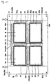
- FIG. 10 is a plan view showing a flat substrate worked by a manufacturing method according to Example 6 of this invention;
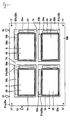
- FIG. 11 is a plan view showing a flat substrate according to a modification of Example 6;
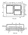
- FIG. 12 is a plan view showing a flat substrate according to another modification of Example 6;
- FIG. 13 is a sectional view showing a vacuum sealing process of a manufacturing method according to Example 7 of this invention;
- FIG. 14 is a plan view showing flat substrates worked by a manufacturing method according to Example 8 of this invention;
- FIG. 15 is a sectional view showing the flat substrates sealed by the manufacturing method according to Example 8;
- FIGS. 16A to 16C are sectional views individually showing cutting and separating processes and a chamfering process for flat substrates in a manufacturing method according to Example 9 of this invention;
- FIG. 17 is a sectional view showing flat substrates according to a modification of Example 9; and
- FIG. 18 is a sectional view showing flat substrates according to another modification of Example 9.
- A method of manufacturing flat display apparatuses according to an embodiment of this invention will now be described in detail with reference to the accompanying drawings.
- As shown in FIGS. 1, 2A and 2B, a
flat display apparatus 10 comprises two rectangularflat substrates image display region 13 provided thereon. Formed on theimage display region 13 are variousimage display patterns 8 for a phosphor screen, color filter, electron sources, plasma cells, drive wiring array, TFT array, etc. - In order to cut off the
image display region 13 from the ambience, theflat substrate 11 and theflat substrate 12 are stuck to each other by means of aframe 7 in asealing region 14 that is situated around theimage display region 13, and are sealed and combined with a given space between them.Drive wires 6 for driving image display elements, such as the electron sources, plasma cells, etc., are led out of the peripheral portion of at least one of theflat substrates drive wires 6 are connected to a drive circuit board (not shown) in positions corresponding to mountingregions - FIGS. 2A and 2B individually show flat display apparatuses of the same configuration and different sizes.
- In manufacturing processes for these flat display apparatuses, there are various incidental elements that are essential to the manufacture of the
flat substrates - Butting
portions 16 for positioning the end faces of the substrate and registermarks 17 for finely adjusting the superposition of a plurality of patterns are used in a working process for theflat substrate 11, such as a printing process or photolithography process as shown in FIG. 3, for example. Used in the manufacturing processes, moreover, are jigs (not shown) for supporting the periphery of theflat substrate 11 and inspection probes (not shown) that touch the mountingregions flat substrate 11 to inspect wiring. - If two types of flat substrates having different sizes, such as the ones shown in FIGS. 2A and 2B, are to be manufactured in common manufacturing processes, however, much manufacturing equipment must be replaced as well as fixing, holding, and transporting devices used in the manufacturing processes, depending on the size difference between the flat substrates. The equipment includes the aforesaid
reference butting portions 16, a mark recognition device, the supporting jigs, the inspection probes, etc. - In the manufacturing method for flat display apparatuses according to the present embodiment, therefore, flat substrates of a common size are prepared for flat display apparatuses of some supposable sizes. The individual manufacturing processes are executed using mechanical, thermal, electrical, and chemical manufacturing equipment that match the flat substrates of the common size. A first region for use as the flat display apparatus and second regions outside the first region are set on each flat substrate. After the first region of a certain size is worked, the second regions are cut and separated, whereupon the flat display apparatus is produced.
- In fabricating flat display apparatuses of different sizes, the first region and its corresponding second regions, having different sizes, are provided on each flat substrate of the common size. By doing this, the flat display apparatuses of different sizes can be manufactured by common manufacturing equipment in the common manufacturing processes. The second regions of the flat substrate are also cut and separated in the case of flat display apparatuses of different sizes. According to this method, the substrates and the manufacturing equipment can be standardized for the image display apparatuses of the individual sizes, so that the flat display apparatuses of different sizes can be easily coped with at low cost. In consequence, the operating efficiency of the manufacturing equipment is improved, so that the manufacturing cost can be lowered.
- As shown in FIG. 4, a
flat substrate 21a that is one size larger thanfirst regions Peripheral regions first regions flat substrate 21a are regarded as second regions. Thus, the manufacturing equipment can be standardized for the manufacture of the flat display apparatuses of several sizes. Since thesecond regions - The necessary width or extent for each second region depends on the design of the manufacturing equipment that is used in common for the region. If it is too large, idle areas increase. Accordingly, the size of each second region must be set deliberately. In manufacturing a small-sized, flat display apparatus by the present manufacturing method, the second regions to be finally cut and separated from the flat substrate is wide. It is appropriate, therefore, to restrict differences in size between the flat image display apparatuses to be manufactured to about 10 inches at the maximum. The manufacture of flat display apparatuses having size differences of more than 10 inches entails an increase in idle areas in the second regions. Thus, an alternative manufacturing line should preferably be used to cope with this.
- The following is a description of a case in which an FED is manufactured as a flat display apparatus, for example.
- The following is a description of a case in which a 35-inch FED is manufactured as FEDs of different sizes ranging from 30 to 40 inches are manufactured in a common manufacturing line.
- First, the rectangular
flat substrate 21a is prepared as a common flat substrate, as shown in FIG. 5. Theflat substrate 21a is given a size of 42 inches, for example. - Subsequently, the rectangular
first region 21b to be used for the 35-inch FED is set on theflat substrate 21a, and this first region is worked as desired. Thus, a rectangularimage display region 23 having theimage display pattern 8, a sealingregion 24 in the form of a rectangular frame situated around the image display region, mountingregions first region 21b. - The
first region 21b is set in the central portion of theflat substrate 21a. Thereupon, thesecond regions first region 21b. All the necessary parts for the manufacture, including the register marks 17, buttingportions 16, etc., are formed in advance in thesecond regions flat substrate 21a, and engaging portions that engage the buttingmembers 16 are located in two spots on one long side of the flat substrate and in one spot on one short side. - The register marks 17 may be located at any points on the
flat substrate 21a, obverse, reverse, inside, or outside. Preferably, the register marks 17 should be located on the end portions: of theflat substrate 21a, e.g., in the four corner portions. After the FED is manufactured, moreover, thesecond regions first region 21b, so that the FED can be reduced to a narrow frame. Further, the flat substrate may be registered by means of the buttingmembers 16 only, without using the register marks 17. - Manufacturing processes for working the
flat substrate 21a, such as printing, photolithography, etc., can cope with sizes of up to 40 inches. In manufacturing processes such as printing, photolithography, etc., theflat substrate 21a is aligned with the manufacturing apparatus with a substrate end face of theflat substrate 21a abutting against the buttingmembers 16 or with reference to the register marks 17 in thesecond regions members 16 and the register marks 17 can be standardized by standardizing the shape of theflat substrate 21a or the positions of the register marks 17 without regard to the size of the FED to be manufactured. Common devices can be also used as the transporting and supporting devices for theflat substrate 21a. - After the desired
image display pattern 8 is formed on thefirst region 21b, theflat substrate 21a is delivered directly to the next process. Depending on the conditions of the manufacturing equipment for the next process, theflat substrate 21a may be delivered to the next process after the peripheralsecond regions - Two desiredly worked
flat substrates 21a are formed individually in the processes described above, and these two flat substrates are stuck to each other with the sealingregion 24 between them. After the FED is completed with the respectivefirst regions 21b of theflat substrates 21a, thesecond regions flat substrates 21a may be stuck together after the useless second regions of one or both of the flat substrates are cut and separated. In this case, the second regions are cut and separated again, thereafter, so that the frame portion of the flat display apparatus is smallest. - The
flat substrate 21a is cut by the following methods. The methods include a scratched portion tensile stress cutting method in which the flat substrate is doubled after it is scratched along the boundaries between thefirst region 21b and thesecond regions - Further, the various parts may be mounted by utilizing the register marks 17 before the
second regions flat substrates 21a of the common size are sealed together. Thereafter, flexible drive wires are mounted on the mounting region of at least one of theflat substrates 21a by using an anisotropic conductive film (ACF), for example. In doing this, the flexible drive wires are mounted by heat-bonding the ACF under pressure after the position of the ACF is adjusted with reference to the register marks 17 in thesecond regions flat substrate 21a. - According to the manufacturing method for the FED constructed in this manner, the
flat substrates 21a of the common size are provided with thefirst regions 21b of different sizes and thesecond regions first regions 21b, so that FEDs of different sizes can be manufactured in by means of the common manufacturing equipment in the common manufacturing processes. Accordingly, the FEDs of different sizes can be easily coped with at low cost. Thus, the operating efficiency of the manufacturing equipment is improved, so that the FEDs can be provided at low cost. - In the manufacturing processes, the
second regions flat substrates 21a, and are set around thefirst regions 21b in common for the individual sizes. Thus, thesecond regions flat substrates 21a that are common to the FEDs of different sizes. By doing this, the manufacturing equipment that are used to support and align the substrates are standardized, and the flat substrates 12a are standardized. Thus, flexible, high-productivity manufacturing processes can be realized. - Further, the
second regions first regions 21b, have good areas, and are finally cut and separated from the first regions. Thus, the manufacturing processes, including processes of holding, fixing, and transporting the substrates, can be carried out securely and safely. At the same time, bad influences of the manufacturing processes on the first regions and the FED fabricating processes, such as temperature irregularity, can be reduced, and the quality and yield of products can be improved. In consequence, narrow-frame FEDs without any useless regions can be realized. - The manufacturing method using the single flat substrate or the two flat substrates has been described in connection with Example 1. In manufacturing a flat display apparatus in which a grid is located between two first regions, for example, however, the same manufacturing method as aforesaid may be applied to the grid.
- In some cases, according to the manufacturing method described above, the manufacturing equipment may be shared, and besides, member shapes for transfer films, protective sheets, sputtering targets, etc. may be standardized.
- According to Example 2, as shown in FIGS. 6A and 6B, various manufacturing processes are carried out with a
first region 21b set near one corner portion of aflat substrate 21a and with use of only twosecond regions - According to Example 3, as shown in FIGS. 7A and 7B,
second regions first region 21b that is situated outside a sealingregion 14 is asymmetric, in order to make the first region as compact as possible. More specifically, the other two side portions of the frame region are made narrower than those two side portions on which mountingregions - According to this manufacturing method, differences that are attributable to differences in size between display apparatuses to be manufactured involve differences in cutting specifications only. Therefore, this example shares load on the manufacturing processes with the other examples even though cutting and the like are made so that the frame region is asymmetric. According to the present example, which shares the same functions and effects with the foregoing alternative examples, the frame of a resulting FED can be further narrowed. This example shares other configurations with the foregoing examples, and a detailed description of them is omitted.
- According to the present example, as shown in FIG. 8,
inspection wiring regions second regions regions flat substrate 21a, during the manufacturing processes. They are formed by leading out wiring portions individually from the mounting regions in an enlarged form. - In subjecting a wiring array to open/short inspection using inspection probes (not shown), therefore, the locations of the inspection probes can be standardized without regard to the size of a
first region 21b. Further, the wiring space is widened, so that the inspection probes can be contacted more securely and introduced more easily. Thus, the inspection time can be shortened, so that the manufacturing efficiency can be improved. - Further, lead-out patterns of the
inspection wiring regions - As another example of application, moreover, the
second regions second regions image display region 23 in a printing process or the like. Improvement on quality control can be made by inspecting this partial print pattern and checking theimage display region 23 for quality or by feeding back the result of inspection to control conditions for the printing process. - According to the present example, moreover, the
second regions image display region 23 that is carried out in various processes, whereupon a plurality of small treated regions are formed side by side in due order in each second region. Further, a control code, such as a bar code for the discriminative recognition of the flat substrate is assigned to each of thesecond regions second regions flat substrate 21a, the control codes can be used to control or inspect the treated regions of the second regions, thus serving for product quality control or analysis of causes of problems, if any. This example shares other configurations with the foregoing examples, and a detailed description of them is omitted. - In a flat display apparatus, such as an FED or SED, the inside of an envelope that is composed of two flat substrates must be kept in a vacuum. Also in a PDP, discharge gas must be charged after the inside of the envelope is temporarily evacuated. A method of evacuating the envelope in this manner includes a manufacturing process in which a front substrate and a rear substrate that constitutes the envelope are finally assembled in a vacuum tank.
- In this case, the front substrate and the rear substrate that are first located in the vacuum tank are heated fully. This is done in order to reduce gas discharge from the inner surfaces of the substrates that constitutes a main cause of lowering of the degree of vacuum of the envelope. When the front substrate and the rear substrate are then cooled so that the degree of vacuum in the vacuum tank is fully enhanced, getter flashing is carried out in the vacuum tank to form a getter film on a phosphor screen, in order to improve and maintain the degree of vacuum of the envelope. Thereafter, the front substrate and the rear substrate are heated again to a temperature such that a sealing material melts, and the front substrate and the rear substrate are lapped together and cooled so that the sealing material solidifies.
- The vacuum envelope fabricated by this method is obtained in a process that combines a getter process, sealing process, and vacuum encapsulation process, and can enjoy a very satisfactory degree of vacuum without requiring any such time for the case where the inside of the envelope is exhausted by means of an exhaust pipe.
- According to the present example, as shown in FIG. 9, two
flat substrates vacuum tank 60 in a manner such that afirst region 51b of theflat substrate 51a and afirst region 52b of theflat substrate 52a are opposed to each other. In order to fix the relative positions of thefirst regions second regions flat substrates -
Image display patterns 8 of theflat substrates camera 19 outside thevacuum tank 60 as thesecond regions members 18. Thereafter, theflat substrates regions 54 by heating theflat substrates heater 47 in thevacuum tank 60. - Thus, the sealing process that is carried out in a vacuum includes many steps that utilize the peripheral portions of the flat substrates, such as the steps of supporting the
flat substrates flat substrates second regions first regions - Although the sealing process has been described in connection with the present example, the same method may be also applied to any other processes of heat treatment in a vacuum. This example shares the manufacturing method for the flat substrates themselves with the foregoing examples, and a detailed description of the method is omitted.
- According to this example, as shown in FIG. 10, a large-sized
flat substrate 51a is provided with four small-sizedfirst regions 51b of the same size, andsecond regions image display region 53, sealingregion 54, and mountingregions first region 51b by the same method for the foregoing examples. - Further, a large-sized
flat substrate 52a is prepared having four small-sizedfirst regions 52b of the same size andsecond regions - These
flat substrates vacuum tank 60 in the same method for Example 5 shown in FIG. 9. The respective end faces of thesecond regions flat substrates - Subsequently, the
flat substrates respective sealing regions 54 of thefirst regions second regions first regions division lines - As shown in FIG. 11, moreover,
second regions first regions second regions flat substrates flat substrates second regions - As shown in FIG. 12, moreover, the
first regions flat substrates - In heating
flat substrates vacuum tank 60, according to Example 7, thevacuum tank 60 is brought into contact with thesecond regions flat substrate 52a, and theflat substrate 52a itself forms one wall of the vacuum tank, as shown in FIG. 13. Further, the peripheral edge portion of theflat substrate 52a projects from thevacuum tank 60 into the atmosphere. - Furthermore, a
decompression tank 61 is located on the backside of theflat substrate 52a, and the inside of the decompression tank is decompressed to about 1/1 to 1/1,000 atm. so that a high atmospheric pressure does not act on theflat substrate 52a. Theflat substrates - According to this arrangement, heat treatment can be carried out with the respective peripheral portions of the
second regions flat substrate 52a exposed to the atmosphere. Thus, failure in thefirst regions vacuum tank 60 can be checked for occurrence from outside the vacuum tank. Further, the rearflat substrate 52a can be placed directly on theheater 47 as it is heated. - If mounting
regions first regions flat substrates flat substrate 51a hassecond regions region 55a is formed. The otherflat substrate 52a hassecond regions first region 52b on which the mountingregion 55b is located. The twoflat substrates second regions flat substrate 51a project from theflat substrate 52a and that thesecond regions flat substrate 52a project from theflat substrate 51a, and these substrates are sealed to each other. - According to the arrangement described above, cut surfaces along which the second regions of each flat substrate are cut and separated are situated at an outside distance from the end faces of the other flat substrate even after the substrates are sealed together. Accordingly, the second regions can be easily cut and separated, and sharp
angular cut portions - In this case, the
second regions flat substrates register marks flat substrates - In order to cope with different sizes, a common length is used for the side length of those sides of the
flat substrates second regions - After the two
flat substrates second region 30a is cut and separated, as shown in FIG. 16B. Thereupon, sharpangular cut portions angular portion 80c on the sealed surface side is situated in a position such that it cannot be chamfered with ease. - According to present example, as shown in FIG. 16C, therefore, the
angular portion 80c is not chamfered. If theangular portion 80c is left unchamfered, it does not result directly in the aforesaid problem, since it is situated in a position that is inaccessible to the outside and cannot be reached by a flexible wiring board. - Methods shown in FIGS. 17 and 18 may be sued as alternative treatment methods for the sharp angular cut portions. In the example shown in FIG. 17, the
angular portion 80c that cannot be chamfered with ease is covered by aprotective material 90. Thus, theangular portion 80c can be prevented from being touched from the outside. - A resin, adhesive agent, putty, or tape is used for the
protective material 90. - In the example shown in FIG. 18, moreover, all the
angular portions protective material 90 without being chamfered at all. Theprotective material 90 serves also to encapsulate a bondedsurface 101 of theflexible wiring board 100. - Normally, the
flexible wiring board 100 is attached to the substrates by being heat-bonded with use of an anisotropic conductive film under pressure. However, the bondedportion 101 that bears proof pressure between wires that are arranged at short pitches or the like is susceptible to external moisture and foreign matter, and is subjected to force when theflexible wiring board 100 is bent. - According to the present example, the
protective material 90 is effective means that can serve both to cover the sharp angular portions and to protect the bondedsurface 101 of theflexible wiring board 100. - This example shares the manufacturing method for the flat substrates themselves with the foregoing examples, and a detailed description of the method is omitted.
- This invention is not limited to the examples described, and various modifications may be effected without departing from the scope of the invention. Although the manufacture of FEDs has been described in connection with the foregoing examples, for example, this invention is not limited to FEDs and may be also applied to the manufacture of any other flat display apparatuses, such as SEDs, PDPs, etc. The dimensions of the flat substrates used, the dimensions and number of first regions to be formed, etc. may be selected as required without being limited to the values described in conjunction with foregoing examples.
- According to an aspect of this invention, flat substrates are given a large common size in manufacturing processes, and useless regions of the flat substrates are finally cut and separated. By doing this, flat display apparatuses of different sizes can be manufactured with use of common substrates and common manufacturing processes. According to an aspect of this invention, there may be provided a manufacturing method for flat display apparatuses such that interference of manufacturing equipment with the manufacturing processes can be reduced and that the flat display apparatuses can be formed having a narrower frame structure.
Claims (27)
- A method of manufacturing flat display apparatuses, in which the flat display apparatuses are manufactured by working flat substrates, the method comprising:preparing a flat substrate having a first region which constitutes a flat display apparatus and second regions outside the first region;working at least the first region; andcutting and separating the second regions from the flat substrate after the working.
- A method of manufacturing flat display apparatuses according to claim 1, wherein the flat substrate used is a flat substrate of a predetermined common size, the first region of one size selected from a plurality of sizes smaller than the common size is formed on the flat substrate of the common size, and the flat display apparatus of the selected one size is manufactured.
- A method of manufacturing flat display apparatuses according to claim 2, wherein the given working is carried out for the first regions of the plurality of sizes by using a common manufacturing apparatus.
- A method of manufacturing flat display apparatuses according to claim 1, wherein the flat substrate has thereon a plurality of first regions which individually form flat display apparatuses.
- A method of manufacturing flat display apparatuses according to claim 4, wherein the flat substrate has thereon a plurality of first regions of the same size which individually form the flat display apparatuses.
- A method of manufacturing flat display apparatuses according to claim 4, wherein the flat substrate has thereon a plurality of first regions of different sizes which individually form the flat display apparatuses.
- A method of manufacturing flat display apparatuses according to claim 1, wherein the flat substrate is rectangular, and the second region is located on end portions along at least one long side and one short side of the flat substrate.
- A method of manufacturing flat display apparatuses according to claim 7, wherein the flat substrate is rectangular, and the second region is located on end portions along four sides of the flat substrate.
- A method of manufacturing flat display apparatuses according to claim 7, wherein the flat substrate has thereon a plurality of first regions which individually constitute flat display apparatuses, and the second region is located so as to cover regions between the first regions.
- A method of manufacturing flat display apparatuses according to claim 1, wherein the first region is located in a central portion of the flat substrate, and the second region is located so as to surround the first region.
- A method of manufacturing flat display apparatuses according to claim 1, wherein the first region is located on a peripheral portion of the flat display apparatus including at least one side thereof.
- A method of manufacturing flat display apparatuses according to claim 1, wherein the working includes forming a substantially rectangular image display region and a frame portion in the first region, the frame portion being situated around the image display region and having a plurality of side portions, and the second region is located so that the respective widths of the side portions of the frame portion are unequal.
- A method of manufacturing flat display apparatuses according to claim 1, wherein the working includes forming a substantially rectangular image display region and a frame portion in the first region, the frame portion being situated around the image display region and having a plurality of side portions, and providing mounting regions individually on at least two side portions of the frame portion so that the width of the other side portions of the frame portion on which the mounting regions are not provided is smaller than the width of the side portions on which the mounting regions are provided.
- A method of manufacturing flat display apparatuses according to claim 1, wherein the working includes supporting and fixing the flat substrate in positions corresponding to the second region.
- A method of manufacturing flat display apparatuses according to claim 1, wherein the flat substrate is aligned with use of end portions of the second region.
- A method of manufacturing flat display apparatuses according to claim 1, wherein the working includes providing specific patterns to be used in the working in the second region.
- A method of manufacturing flat display apparatuses according to claim 16, wherein the specific patterns include wiring patterns led out through the first region, and the flat substrate is worked and inspected with use of the specific patterns.
- A method of manufacturing flat display apparatuses according to claim 16, wherein the flat substrate and the formed flat display apparatus are worked and controlled in quality in accordance with the specific patterns.
- A method of manufacturing flat display apparatuses according to claim 18, wherein the specific patterns includes control codes for the flat display apparatus, and quality control for the flat display apparatus is carried out with use of the specific patterns and the control codes in the cut and separated second region after the second region is removed by cutting.
- A method of manufacturing flat display apparatuses according to claim 1, wherein the working includes working in a vacuum.
- A method of manufacturing flat display apparatuses according to claim 20, wherein the working in the vacuum includes a heat treatment for the flat substrate.
- A method of manufacturing flat display apparatuses according to claim 20, wherein the working in the vacuum includes forming a getter film in the first region by getter flashing in the vacuum.
- A method of manufacturing flat display apparatuses according to claim 20, wherein two flat substrates are prepared each having the first region and the second region, and the two flat substrates are sealed to each other in the vacuum after the respective first regions of the flat substrates are subjected to the working.
- A method of manufacturing flat display apparatuses according to claim 22, wherein one flat substrate, out of the two flat substrates, is provided with second regions outside two long sides of the first region thereof, and the other flat substrate is provided with second regions outside two short sides of the first region thereof.
- A method of manufacturing flat display apparatuses according to claim 1, wherein two flat substrates are prepared each having the first region and the second region, and the working includes sealing the two flat substrates, each having the first and second regions, to each other and covering a cut-side end portion of at least one of the flat substrates, from which the second region is separated, with a protective material after the sealing.
- A method of manufacturing flat display apparatuses according to claim 25, wherein the working includes forming a substantially rectangular image display region and a frame portion in the first region, the frame portion being situated around the image display region and having a plurality of side portions, providing mounting regions individually on at least two side portions of the frame portion, adhesively bonding flexible wiring boards to at least two side portions of the frame portion, and encapsulating bonded regions of the flexible wiring boards with the protective material.
- A method of manufacturing flat display apparatuses according to claim 1, wherein the flat display apparatus is a field emission display or a surface-conduction emitter display.
Applications Claiming Priority (3)
| Application Number | Priority Date | Filing Date | Title |
|---|---|---|---|
| JP2001398183A JP2003197103A (en) | 2001-12-27 | 2001-12-27 | Method for manufacturing flat display device |
| JP2001398183 | 2001-12-27 | ||
| PCT/JP2002/013526 WO2003056533A1 (en) | 2001-12-27 | 2002-12-25 | Production method for plane-type display unit |
Publications (2)
| Publication Number | Publication Date |
|---|---|
| EP1460607A1 true EP1460607A1 (en) | 2004-09-22 |
| EP1460607A4 EP1460607A4 (en) | 2006-09-20 |
Family
ID=19189288
Family Applications (1)
| Application Number | Title | Priority Date | Filing Date |
|---|---|---|---|
| EP02793384A Withdrawn EP1460607A4 (en) | 2001-12-27 | 2002-12-25 | Production method for plane-type display unit |
Country Status (7)
| Country | Link |
|---|---|
| US (2) | US7273403B2 (en) |
| EP (1) | EP1460607A4 (en) |
| JP (1) | JP2003197103A (en) |
| KR (1) | KR100713729B1 (en) |
| CN (1) | CN1322480C (en) |
| TW (1) | TWI284914B (en) |
| WO (1) | WO2003056533A1 (en) |
Families Citing this family (38)
| Publication number | Priority date | Publication date | Assignee | Title |
|---|---|---|---|---|
| JP2003197103A (en) * | 2001-12-27 | 2003-07-11 | Toshiba Corp | Method for manufacturing flat display device |
| KR100414914B1 (en) * | 2002-03-05 | 2004-01-13 | 삼성전자주식회사 | Wide band erbium doped fiber amplifier with gain enhancement |
| US7285914B2 (en) * | 2003-11-13 | 2007-10-23 | Samsung Sdi Co., Ltd. | Plasma display panel (PDP) having phosphor layers in non-display areas |
| JP4376597B2 (en) * | 2003-11-26 | 2009-12-02 | 日立プラズマディスプレイ株式会社 | Flat panel display |
| KR100966430B1 (en) * | 2004-08-31 | 2010-06-28 | 엘지디스플레이 주식회사 | Soft baking apparatus having a substrate support pin and soft baking method using the same |
| JP4686154B2 (en) * | 2004-09-14 | 2011-05-18 | 大日本印刷株式会社 | Manufacturing method of display element substrate |
| US8603288B2 (en) | 2008-01-18 | 2013-12-10 | Rockwell Collins, Inc. | Planarization treatment of pressure sensitive adhesive for rigid-to-rigid substrate lamination |
| US8118075B2 (en) * | 2008-01-18 | 2012-02-21 | Rockwell Collins, Inc. | System and method for disassembling laminated substrates |
| US8936057B2 (en) * | 2005-08-30 | 2015-01-20 | Rockwell Collins, Inc. | Substrate lamination system and method |
| US7814676B2 (en) * | 2008-01-18 | 2010-10-19 | Rockwell Collins, Inc. | Alignment system and method thereof |
| US8137498B2 (en) | 2005-08-30 | 2012-03-20 | Rockwell Collins Inc. | System and method for completing lamination of rigid-to-rigid substrates by the controlled application of pressure |
| US8691043B2 (en) * | 2005-08-30 | 2014-04-08 | Rockwell Collins, Inc. | Substrate lamination system and method |
| KR100879296B1 (en) * | 2006-04-20 | 2009-01-16 | 삼성에스디아이 주식회사 | Vacuum container for display device, manufacturing method of vacuum container, and electron emission display device using vacuum container |
| US7461564B2 (en) * | 2006-10-04 | 2008-12-09 | Corning Incorporated | Method and apparatus for proof testing a sheet of brittle material |
| US9733349B1 (en) | 2007-09-06 | 2017-08-15 | Rockwell Collins, Inc. | System for and method of radar data processing for low visibility landing applications |
| US9939526B2 (en) | 2007-09-06 | 2018-04-10 | Rockwell Collins, Inc. | Display system and method using weather radar sensing |
| WO2009091923A2 (en) | 2008-01-18 | 2009-07-23 | Rockwell Collins, Inc. | Substrate lamination system and method |
| JP2011048012A (en) * | 2009-08-25 | 2011-03-10 | Citizen Finetech Miyota Co Ltd | Liquid crystal display device |
| ES2450520T5 (en) | 2010-03-05 | 2017-08-07 | Sage Electrochromics, Inc. | Laminated electrochromic device to glass substrates |
| US8411235B1 (en) | 2010-03-16 | 2013-04-02 | Rockwell Collins, Inc. | Displays for three-dimensional imaging |
| US8419496B1 (en) | 2010-03-18 | 2013-04-16 | Rockwell Collins, Inc. | Display panel alignment system |
| US8486535B1 (en) | 2010-05-24 | 2013-07-16 | Rockwell Collins, Inc. | Systems and methods for adherable and removable thin flexible glass |
| US8576370B1 (en) | 2010-06-30 | 2013-11-05 | Rockwell Collins, Inc. | Systems and methods for nonplanar laminated assemblies |
| FR2962682B1 (en) | 2010-07-16 | 2015-02-27 | Saint Gobain | ELECTROCHEMICAL WINDOW WITH ELECTRONICALLY CONTROLLED OPTICAL AND / OR ENERGY PROPERTIES |
| CN102169260B (en) | 2010-10-15 | 2015-01-21 | 京东方科技集团股份有限公司 | TFT-LCD (thin film transistor liquid crystal display) pixel electrode layer structure, preparation method and mask plate thereof |
| US8643260B1 (en) | 2011-09-02 | 2014-02-04 | Rockwell Collins, Inc. | Systems and methods for display assemblies having printed masking |
| US9272941B2 (en) | 2012-04-05 | 2016-03-01 | Sage Electrochromics, Inc. | Method of cutting a panel using a starter crack and a glass panel including a starter crack |
| US8647727B1 (en) | 2012-06-29 | 2014-02-11 | Rockwell Colllins, Inc. | Optical assembly with adhesive layers configured for diffusion |
| JP2014160201A (en) * | 2013-02-20 | 2014-09-04 | Sumitomo Chemical Co Ltd | Method for manufacturing optical sheet |
| US9262932B1 (en) | 2013-04-05 | 2016-02-16 | Rockwell Collins, Inc. | Extended runway centerline systems and methods |
| US9809491B2 (en) * | 2013-09-09 | 2017-11-07 | Shenzhen China Star Optoelectronics Technology Co., Ltd. | Device and method for baking substrate |
| US9981460B1 (en) | 2014-05-06 | 2018-05-29 | Rockwell Collins, Inc. | Systems and methods for substrate lamination |
| CN104102051B (en) * | 2014-06-30 | 2016-08-17 | 京东方科技集团股份有限公司 | A kind of motherboard of liquid crystal display to cassette method, the liquid crystal display substrate of off-standard size |
| US10928510B1 (en) | 2014-09-10 | 2021-02-23 | Rockwell Collins, Inc. | System for and method of image processing for low visibility landing applications |
| KR102293124B1 (en) * | 2015-04-29 | 2021-08-24 | 삼성디스플레이 주식회사 | Method of manufacturing display device |
| US10705201B1 (en) | 2015-08-31 | 2020-07-07 | Rockwell Collins, Inc. | Radar beam sharpening system and method |
| US10228460B1 (en) | 2016-05-26 | 2019-03-12 | Rockwell Collins, Inc. | Weather radar enabled low visibility operation system and method |
| US10353068B1 (en) | 2016-07-28 | 2019-07-16 | Rockwell Collins, Inc. | Weather radar enabled offshore operation system and method |
Family Cites Families (33)
| Publication number | Priority date | Publication date | Assignee | Title |
|---|---|---|---|---|
| US3960534A (en) * | 1974-04-29 | 1976-06-01 | Rca Corporation | Method of assembling a liquid crystal cell |
| US4195892A (en) * | 1978-06-01 | 1980-04-01 | International Business Machines Corporation | Batch production of plasma display panels |
| JPS60111068U (en) * | 1983-12-28 | 1985-07-27 | アルプス電気株式会社 | flexible printed circuit board |
| US4691995A (en) * | 1985-07-15 | 1987-09-08 | Semiconductor Energy Laboratory Co., Ltd. | Liquid crystal filling device |
| JPH0389431A (en) * | 1989-08-31 | 1991-04-15 | Nec Kansai Ltd | Manufacture of fluorescent panel |
| JPH04149926A (en) * | 1990-10-15 | 1992-05-22 | Nec Corp | Manufacture of plasma display panel and seasoning method thereof |
| JPH04163422A (en) * | 1990-10-26 | 1992-06-09 | Seikosha Co Ltd | Manufacture for liquid crystal panel |
| US5592199A (en) * | 1993-01-27 | 1997-01-07 | Sharp Kabushiki Kaisha | Assembly structure of a flat type device including a panel having electrode terminals disposed on a peripheral portion thereof and method for assembling the same |
| US5686790A (en) * | 1993-06-22 | 1997-11-11 | Candescent Technologies Corporation | Flat panel device with ceramic backplate |
| JPH07318879A (en) * | 1994-05-20 | 1995-12-08 | Casio Comput Co Ltd | Liquid crystal display device manufacturing method |
| TW378276B (en) * | 1995-01-13 | 2000-01-01 | Seiko Epson Corp | Liquid crystal display device and its fabrication method |
| CN1136215A (en) * | 1995-02-28 | 1996-11-20 | 社团法人高等技术研究院研究组合 | Field emission display |
| JPH08328486A (en) * | 1995-05-29 | 1996-12-13 | Canon Inc | Image forming apparatus manufacturing method |
| JPH09244547A (en) * | 1996-03-12 | 1997-09-19 | Toshiba Corp | Display device manufacturing method |
| JPH09305125A (en) * | 1996-05-13 | 1997-11-28 | Noritake Co Ltd | Image display element and seal spacer |
| CN1145914C (en) * | 1996-07-08 | 2004-04-14 | 三星电管株式会社 | field emission display device |
| JPH1195231A (en) | 1997-09-22 | 1999-04-09 | Toshiba Electronic Engineering Corp | Liquid crystal display |
| GB9721804D0 (en) * | 1997-10-15 | 1997-12-17 | Gec Marconi Avionics Holdings | Improvements in or relating to liquid crystal displays |
| JPH11119204A (en) * | 1997-10-16 | 1999-04-30 | Toray Ind Inc | Substrate with color filter |
| JPH11295755A (en) * | 1998-04-09 | 1999-10-29 | Seiko Epson Corp | Wiring board inspection method and liquid crystal device manufacturing method |
| JPH11305201A (en) * | 1998-04-17 | 1999-11-05 | Sharp Corp | Liquid crystal display |
| JP2000010111A (en) | 1998-06-19 | 2000-01-14 | Sharp Corp | Production of electrode substrate |
| JP2000162990A (en) | 1998-11-27 | 2000-06-16 | Seiko Epson Corp | Method for manufacturing display device |
| JP2000193950A (en) * | 1998-12-28 | 2000-07-14 | Optrex Corp | Manufacture of interference panel for stn type liquid crystal display element |
| JP3619085B2 (en) * | 1999-02-18 | 2005-02-09 | キヤノン株式会社 | Image forming apparatus, manufacturing method thereof, and storage medium |
| JP4372260B2 (en) * | 1999-03-17 | 2009-11-25 | シャープ株式会社 | Manufacturing method of liquid crystal panel |
| KR20010001152A (en) | 1999-06-02 | 2001-01-05 | 윤종용 | A test apparatus for testing liquid crystal display |
| KR20010001152U (en) * | 1999-06-25 | 2001-01-15 | 김순택 | Sealing structure of LCD |
| KR100720066B1 (en) * | 1999-11-09 | 2007-05-18 | 가부시키가이샤 한도오따이 에네루기 켄큐쇼 | Method of manufacturing a light emitting device |
| JP2001266768A (en) * | 2000-03-15 | 2001-09-28 | Matsushita Electric Works Ltd | Surface emission plate, method of producing plane luminescent plate, flat crt display, and field emission display |
| JP2001305568A (en) * | 2000-04-21 | 2001-10-31 | Matsushita Electric Ind Co Ltd | LCD module |
| JP2002023173A (en) * | 2000-07-03 | 2002-01-23 | Minolta Co Ltd | Manufacturing method of liquid crystal display element |
| JP2003197103A (en) * | 2001-12-27 | 2003-07-11 | Toshiba Corp | Method for manufacturing flat display device |
-
2001
- 2001-12-27 JP JP2001398183A patent/JP2003197103A/en active Pending
-
2002
- 2002-12-25 WO PCT/JP2002/013526 patent/WO2003056533A1/en not_active Ceased
- 2002-12-25 EP EP02793384A patent/EP1460607A4/en not_active Withdrawn
- 2002-12-25 KR KR1020047009993A patent/KR100713729B1/en not_active Expired - Fee Related
- 2002-12-25 TW TW091137321A patent/TWI284914B/en not_active IP Right Cessation
- 2002-12-25 CN CNB028260945A patent/CN1322480C/en not_active Expired - Fee Related
-
2004
- 2004-06-25 US US10/875,400 patent/US7273403B2/en not_active Expired - Fee Related
-
2007
- 2007-05-14 US US11/748,043 patent/US20070212971A1/en not_active Abandoned
Also Published As
| Publication number | Publication date |
|---|---|
| TWI284914B (en) | 2007-08-01 |
| CN1322480C (en) | 2007-06-20 |
| JP2003197103A (en) | 2003-07-11 |
| CN1608277A (en) | 2005-04-20 |
| WO2003056533A1 (en) | 2003-07-10 |
| TW200301916A (en) | 2003-07-16 |
| US20040233156A1 (en) | 2004-11-25 |
| EP1460607A4 (en) | 2006-09-20 |
| US20070212971A1 (en) | 2007-09-13 |
| US7273403B2 (en) | 2007-09-25 |
| KR20040064308A (en) | 2004-07-16 |
| KR100713729B1 (en) | 2007-05-04 |
Similar Documents
| Publication | Publication Date | Title |
|---|---|---|
| US7273403B2 (en) | Method of manufacturing flat display panels of different sizes from a common base substrate | |
| CN1210749C (en) | Method and apparatus for sealing a visual display | |
| US6323590B1 (en) | Wall assembly and method for attaching walls for flat panel display | |
| US6848964B1 (en) | Sealing method and apparatus for manufacturing high-performance gas discharge panel | |
| JP3270054B2 (en) | Field emission device with internal structure for aligning phosphor pixels with corresponding field emitters | |
| US20020079839A1 (en) | Sealing vessel, method for manufacturing thereof and a display apparatus using such sealing vessel | |
| US20080001619A1 (en) | Display panel lighting test apparatus, and test line employing the same | |
| US6356013B1 (en) | Wall assembly and method for attaching walls for flat panel display | |
| US4195892A (en) | Batch production of plasma display panels | |
| JPH10269935A (en) | Panel display manufacturing method and manufacturing apparatus | |
| JP3550027B2 (en) | Manufacturing method of flat display panel | |
| US6249266B1 (en) | Fluorescent display device and process for manufacturing same | |
| JP3943999B2 (en) | Method for forming spacer of flat display element | |
| JPH10199451A (en) | Panel structure of display device | |
| JP2003132823A (en) | Flat display device and method of manufacturing the same | |
| KR20000000636A (en) | Plat panel display having spacer being strengthened supporting state and manufacturing method of the same | |
| JP2008204854A (en) | Manufacturing method of flat display panel | |
| JPH08328486A (en) | Image forming apparatus manufacturing method | |
| JP2007155893A (en) | Method for manufacturing light-shielding mask, and light-shielding mask | |
| JPH01216317A (en) | Manufacture of liquid crystal display panel | |
| JP2003016937A (en) | Plate alignment method for flat panel display and flat panel display | |
| JPH08236041A (en) | Flat display | |
| WO2005122207A1 (en) | Image display device | |
| KR20060060433A (en) | Exposure apparatus for plasma display panel manufacturing | |
| JPH04357653A (en) | Flat panel image display device and its manufacturing method |
Legal Events
| Date | Code | Title | Description |
|---|---|---|---|
| PUAI | Public reference made under article 153(3) epc to a published international application that has entered the european phase |
Free format text: ORIGINAL CODE: 0009012 |
|
| 17P | Request for examination filed |
Effective date: 20040625 |
|
| AK | Designated contracting states |
Kind code of ref document: A1 Designated state(s): DE FR GB IT NL |
|
| AX | Request for extension of the european patent |
Extension state: AL LT LV MK RO |
|
| A4 | Supplementary search report drawn up and despatched |
Effective date: 20060821 |
|
| STAA | Information on the status of an ep patent application or granted ep patent |
Free format text: STATUS: THE APPLICATION HAS BEEN WITHDRAWN |
|
| 18W | Application withdrawn |
Effective date: 20080211 |