EP1455376A2 - Electron-emitting device, electron source, and image display apparatus - Google Patents
Electron-emitting device, electron source, and image display apparatus Download PDFInfo
- Publication number
- EP1455376A2 EP1455376A2 EP04005148A EP04005148A EP1455376A2 EP 1455376 A2 EP1455376 A2 EP 1455376A2 EP 04005148 A EP04005148 A EP 04005148A EP 04005148 A EP04005148 A EP 04005148A EP 1455376 A2 EP1455376 A2 EP 1455376A2
- Authority
- EP
- European Patent Office
- Prior art keywords
- electron
- emitting
- gate electrode
- cathode electrode
- end portions
- Prior art date
- Legal status (The legal status is an assumption and is not a legal conclusion. Google has not performed a legal analysis and makes no representation as to the accuracy of the status listed.)
- Granted
Links
Images


Classifications
-
- B—PERFORMING OPERATIONS; TRANSPORTING
- B82—NANOTECHNOLOGY
- B82Y—SPECIFIC USES OR APPLICATIONS OF NANOSTRUCTURES; MEASUREMENT OR ANALYSIS OF NANOSTRUCTURES; MANUFACTURE OR TREATMENT OF NANOSTRUCTURES
- B82Y10/00—Nanotechnology for information processing, storage or transmission, e.g. quantum computing or single electron logic
-
- E—FIXED CONSTRUCTIONS
- E02—HYDRAULIC ENGINEERING; FOUNDATIONS; SOIL SHIFTING
- E02B—HYDRAULIC ENGINEERING
- E02B5/00—Artificial water canals, e.g. irrigation canals
- E02B5/02—Making or lining canals
-
- H—ELECTRICITY
- H01—ELECTRIC ELEMENTS
- H01J—ELECTRIC DISCHARGE TUBES OR DISCHARGE LAMPS
- H01J1/00—Details of electrodes, of magnetic control means, of screens, or of the mounting or spacing thereof, common to two or more basic types of discharge tubes or lamps
- H01J1/02—Main electrodes
- H01J1/30—Cold cathodes, e.g. field-emissive cathode
- H01J1/304—Field-emissive cathodes
-
- H—ELECTRICITY
- H01—ELECTRIC ELEMENTS
- H01J—ELECTRIC DISCHARGE TUBES OR DISCHARGE LAMPS
- H01J3/00—Details of electron-optical or ion-optical arrangements common to two or more basic types of discharge tubes or lamps
- H01J3/02—Electron guns
- H01J3/021—Electron guns using a field emission, photo emission, or secondary emission electron source
- H01J3/022—Electron guns using a field emission, photo emission, or secondary emission electron source with microengineered cathode, e.g. Spindt-type
-
- H—ELECTRICITY
- H01—ELECTRIC ELEMENTS
- H01J—ELECTRIC DISCHARGE TUBES OR DISCHARGE LAMPS
- H01J2201/00—Electrodes common to discharge tubes
- H01J2201/30—Cold cathodes
- H01J2201/304—Field emission cathodes
- H01J2201/30446—Field emission cathodes characterised by the emitter material
- H01J2201/30453—Carbon types
- H01J2201/30469—Carbon nanotubes (CNTs)
-
- H—ELECTRICITY
- H01—ELECTRIC ELEMENTS
- H01J—ELECTRIC DISCHARGE TUBES OR DISCHARGE LAMPS
- H01J2329/00—Electron emission display panels, e.g. field emission display panels
Definitions
- the present invention relates to an electron-emitting device having a film containing an electron-emitting material, an electron source in which a large number of electron-emitting devices are arranged, and an image display apparatus using the electron source.
- a carbon fiber such as a carbon nanotube (hereinafter referred to as a "CNT") serving as a cold cathode material is attracting attention.
- the carbon nanotube is a fullerene having a cylindrical structure in which graphite of several layers or a single layer is wound, and is a new carbon material discovered in 1991 (Nature, 354, (1991) 56). Further, an application of a carbon nanotube to an image display apparatus using an electron source in which a large number of minute electron-emitting devices are two-dimensionally formed is being attempted.
- the above-mentioned Spindt type electron-emitting device utilizes an electron field emission from a sharpened tip portion of a cathode electrode.
- a carbon fiber such as a CNT has a shape of a high aspect ratio with a minute diameter of several tens of nm and a length of several hundreds of nm to several ⁇ m. Therefore, when the carbon fiber is used for the electron source, it can be driven at low voltage. In addition, because a large allowable current capacity is obtained, the carbon fiber has a large number of characteristics such as a stable large emission current, which are advantageous on an application to the image display apparatus (for example, see Japanese Patent Application Laid-Open No. 2002-025477).
- an example of an electron-emitting device having a lateral structure for example, see US 4728851 and US 4904895.
- a cathode electrode whose tip is sharpened and a gate electrode to extract electrons from the tip of the cathode electrode are formed parallel to a substrate.
- An anode electrode is located in a direction perpendicular to a direction along which the gate electrode and the cathode electrode are opposed.
- an image forming apparatus can be constructed in combination with an image forming member composed of a phosphor and the like.
- a conventional electron source composed of the lateral type electron-emitting device using the carbon fiber such as the carbon nanotube for the electron-emitting region has the following problems.
- Fig. 9 shows an example of the lateral type electron-emitting device.
- Fig. 9 is a plan view when the lateral type electron-emitting device is viewed from above the surface of a base, in which reference numeral 91 denotes a substrate, 92 denotes a cathode electrode, 93 denotes a gate electrode, and 94 denotes an electron-emitting film.
- the electron-emitting film 94 which includes a plurality of carbon fibers, patterned along an edge of the cathode electrode 92 opposed to the gate electrode 93 is formed on the cathode electrode 92.
- the presence or absence of the electron emission from the electron-emitting film 94 is determined according to the electric field strength effectively applied to an electron-emitting part of the carbon fiber. More specifically, this is determined according to (1) a macro electric field strength in accordance with a distance from the opposite gate electrode and (2) an electric field enhancing effect specified by, for example, a shape of the carbon fiber.
- Fig. 10 is a schematic cross sectional view of the electron-emitting device shown in Fig. 9 along the edge portion of the cathode electrode 92.
- a structure of the carbon fiber and a formation density thereof can be made relatively uniform.
- the edge portions 95 are formed at the edge regions of the patterned area. In the edge portions 95, the electric field enhancing effect resulting from electric field concentration generally becomes larger, so that a threshold voltage to the electron emission reduces.
- An object of the present invention is to provide an electron-emitting device, and an electron source, which can be used to manufacture an image forming apparatus having a superior display quality and in which the development of the abnormal light emission point is suppressed and the non-uniformity of brightness is not caused.
- the present invention has been made by an earnest study to solve the above-mentioned problems and is provided through the following electron-emitting device.
- an electron-emitting device is characterized in that:
- an electron-emitting device is characterized in that:
- an electron-emitting device is characterized in that:
- an electron-emitting device is characterized in that:
- an electron-emitting device is characterized in that:
- a plurality of fibrous conductive materials may be used.
- a film mainly containing carbon may be used as the film containing the electron-emitting material.
- a plurality of carbon fibers may be used as the film containing the electron-emitting material.
- each of the plurality of carbon fibers may be one of a carbon nanotube, a graphite nanofiber, an amorphous carbon fiber, and a diamond fiber.
- an electron source including a plurality of electron-emitting devices, each of which is constructed according to the present invention as described above.
- an image display apparatus including:
- an electron-emitting device in which an electron-emitting characteristic distribution in the electron-emitting region is small and to reduce a variation in electron-emitting characteristic between electron-emitting devices. Therefore, by using electron source in which a plurality of electron-emitting devices according to the present invention are arranged, an image forming apparatus capable of uniformly displaying an image having a preferable quality on a large area is obtained.
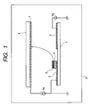
- Fig. 1 is a schematic view showing a state in which an anode electrode 7 is provided opposite to a substrate 1 of the electron-emitting device(2,3,4 and 5), and the electron-emitting device and the anode electrode 7 are set in a vacuum vessel 8.
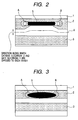
- Fig. 2 is a schematic view showing an example of the electron-emitting device according to the present invention when it is viewed from above the substrate.
- reference numeral 1 denotes a substrate (base); 2, a cathode electrode (negative electrode); 3, a gate electrode (extraction electrode); 4, a conductive layer; 5, a film containing an electron-emitting material (hereinafter referred to as "electron-emitting film”); 6, an anode substrate; 7, an anode electrode; and 8, a vacuum vessel.
- the vacuum vessel 8 is connected with a vacuum evacuation apparatus (not shown).
- a structure including the cathode electrode 2 and the conductive layer 4 is called the cathode electrode.
- the electron-emitting film 5 has two end portions A and B in a plane substantially parallel to a surface of the substrate 1 in a direction substantially perpendicular to a direction along which the cathode electrode 2 and the gate electrode 3 are opposed to each other.
- the electron emissions from the two end portions A and B of the electron-emitting film 5 may be suppressed, so that the electron emission from the region between the two end portions A and B can be controlled.
- any structure may be adopted for the electron-emitting device according to the present invention as long as it is a structure in which the electric field strengths applied between each of the end portions A and B of the electron-emitting film 5 and the gate electrode 3 are made weaker than the electric field strength applied between the region between the two end portions A and B of the electron-emitting film 5 and the gate electrode 3 (such a structure will hereinafter be referred to as "electric field control structure").
- FIGs. 2 to 7 Specific examples of the electric field control structure according to the present invention are shown in Figs. 2 to 7.
- the structures of the electron-emitting devices shown in Figs. 2 to 7 are only examples of the present invention. Note that, in Figs. 2 to 7, the same references are provided to the same members.
- the above-mentioned electric field control structure according to the present invention can be realized by:
- High melting glass such as quartz may be used for the substrate 1.
- the cathode electrode 2 and the gate electrode 3 are formed on the substrate 1 and a catalytic layer is formed in a desired region on the cathode electrode 2.
- a catalytic material containing metal such as Fe, Co, Ni, or Pd, an alloy containing the catalytic material, or the like can be used for the catalytic layer.
- Pd or Co it is preferable to use an alloy of Pd and Co.
- the conductive layer 4 as shown in Fig. 1 is provided between the cathode electrode 2 and the catalytic layer.
- a metallic nitride or a metallic oxide can be used for the conductive layer and a function of easily forming the electron-emitting material in a later step can be provided thereto in some cases.
- an organic gas is introduced into the vacuum vessel 8, so that a plurality of carbon fibers are formed in a region in which the catalytic layer is formed.
- the carbon fibers serve as the electron-emitting material.
- the carbon fiber depending on the temperature during growing, the kind of organic gas, the concentration of the organic gas, and the like, has in many cases a diameter of the order of 5 nm to 250 nm and a length of the order of several tens of nm to several ⁇ m and is fibrously extended while being partially bent (or straightened in some condition).
- a thickness of the film composed of the plurality of carbon fibers is equal to or smaller than an average distance between the gate electrode 3 and the cathode electrode 2, with respect to the controllability of the electric field. Note that, when the above-mentioned heating temperature is further increased, a so-called carbon nanotube can be also formed.
- a conductive fibrous material is easy to obtain a large aspect ratio (length-to-width) and to enhance an electric field, so that electrons can be emitted at low voltage(driving voltage). Therefore, such a material is preferably used as the electron-emitting material according to the present invention.
- the "carbon fiber” according to the present invention can be also called a “columnar substance containing mainly carbon” or a “linear substance containing mainly carbon”.
- the "carbon fiber” can be also called a “fiber containing mainly carbon”. More specifically, the "carbon fiber” according to the present invention includes a carbon nanotube, a graphite nanofiber, an amorphous carbon fiber, and a diamond fiber.
- a structure of the carbon fiber is described in, for example, Japanese Patent Application Laid-Open No. 2000-075167.
- the cylindrical form of graphene (multiple cylindrical structure is called a multi-wall nanotube) is called a carbon nanotube, and its threshold minimizes in a structure in which the distal end of the tube is open.
- the carbon nanotube is a fibrous substance in which graphen is located so as to surround (cylindrically) the longitudinal axis (fiber axis).
- the carbon nanotube is a fibrous substance in which graphen is located substantially parallel to the fiber axis.
- a fibrous substance in which graphenes are stacked in the longitudinal direction (fiber axial direction) is called a "graphite nanofiber”.
- the graphite nanofiber is a fibrous substance composed of a stacked graphens in which each graphene is being arranged so as not to be parallel to the fiber axis(in which each c-axis of the stacked graphens is being arranged so as not to be perpendicular to the fiber axis).
- the "c-axis" indicates a direction in which graphenes are stacked.
- graphite One plane (sheet) of graphite is called a "graphen” or a “graphen sheet”. More specifically, graphite includes stacked carbon planes. Each of carbon planes has equilateral hexagons which are formed by a covalent bond produced by sp2 hybridization of carbon atoms and arranged so as to be laid. A distance between the adjacent carbon planes is about 3.354 angstroms. Each of carbon planes is called a “graphen” or a “graphen sheet”.
- any of the above carbon fibers has an electron-emitting threshold of the order of 1 V/ ⁇ m to 10 V/ ⁇ m and is preferable as the material of an emitter (electron-emitting film 5) according to the present invention.
- an electron-emitting material using a graphite nanofiber is preferably used because it can emit electrons at low electric field, obtain a large emission current, obtain a stable electron-emitting characteristic, and can be easily produced.
- the above-mentioned carbon fiber can be formed by decomposing a hydrocarbon gas using the catalyst (material which promotes depositing of carbon).
- the carbon nanotube and the graphite nanofiber are different from each other with respect to the type of catalyst and the decomposition temperature.
- a graphite nanofiber can be generated at low temperature (temperature of 400°C or higher).
- the generation temperature of a carbon nanotube in the case of using Fe or/and Co is 800°C or higher
- a graphite nanofiber material can be formed at low temperature in the case of using Pd or/and Ni. Therefore, the use of Pd or/and Ni is preferable in views of the influence on other members and the manufacturing cost.
- hydrocarbon gas such as acetylene, ethylene, methane, propane, and propylene
- a CO gas such as a CO 2 gas
- an organic solvent such as ethanol or acetone
- a relative positional relationship between a plane which is a portion of the surface of the electron-emitting film 5, which includes an electron-emitting region, and which is substantially parallel to the surface of the substrate 1, and a plane which includes a portion of the surface of the gate electrode 3 and is substantially parallel to the surface of the substrate 1, is not particularly specified using the substrate surface as reference.
- These planes may be located in substantially the same plane. Even if the planes are located at separate positions, they can be applied to the electric field control structure according to the present invention. Note that, when the planes are located at separate positions, it is necessary to suppress scattering of emitted electrons on the gate electrode 3. Therefore, as shown in Fig.
- the plane which includes the portion of the surface of the electron-emitting film 5 and is substantially parallel to the surface of the substrate 1 is located between the anode electrode 7 and the plane which includes the portion of the surface of the gate electrode 3 and is substantially parallel to the surface of the substrate 1.
- the rate at which electrons emitted from the cathode electrode 2 side collide with the gate electrode 3 can be reduced.
- an electron-emitting device having small spread of emitted electron beams and high efficiency is obtained.
- Fig. 1 first, the electron-emitting device is set in the vacuum vessel 8 and a vacuum state is produced therein using an evacuation apparatus (not shown). Next, a voltage is applied such that the gate electrode 3 has a higher potential than the electron-emitting film 5 (or the cathode electrode 2).
- the electron-emitting device has the structure in which electric fields near the two end portions A and B of the electron-emitting film 5 (see Fig. 2) are weaker than an electric field at the region between the two end portions A and B. Therefore, the electron emission can be preferentially produced at an arbitrary region between the two end portions A and B.
- a region having higher film uniformity of the electron-emitting film can be selectively used as the electron-emitting region by changing the shapes of the electrodes. Therefore, it is possible to provide an electron-emitting device having a uniform electron-emitting characteristic without improving the alignment precision of the electron-emitting film 5.
- an image display apparatus such as a display can be constructed.
- the non-uniformity of brightness in each pixel can be reduced, with the result that the non-uniformity of brightness in the entire display region can be reduced.
- Fig. 2 shows the electron-emitting device according to Example 1 when it is viewed from above the base surface.
- reference numeral 1 denotes the substrate; 2, the cathode electrode; 3, the gate electrode; and 5, the electron-emitting film.
- the conductive layer 4 (not shown) is inserted between the cathode electrode 2 and the electron-emitting film 5, and a combination of the cathode electrode 2 and the conductive layer 4 is called the cathode electrode.
- quartz is used for the substrate 1
- Pt is used for the cathode electrode 2 and the gate electrode 3
- a graphite nanofiber is used for the electron-emitting film 5
- TiN is used for the conductive layer 4.
- the conductive layer 4 and the electron-emitting film 5 are formed in substantially the same region.
- the conductive layer 4 may be formed so as to include a formation region of the electron-emitting film 5.
- the electron-emitting film 5 is patterned in a strip shape with a predetermined width, and the two end portions A and B exist in the longitudinal direction of the strip.
- the space between the gate electrode 3 and the cathode electrode 2 is not constant.
- the space in the region between the two end portions of the electron-emitting film 5 is wider than the space in the vicinities of the two end portions of the electron-emitting film 5. Therefore, a distance between the end of the cathode electrode 2 and the electron-emitting film 5 is relatively large in each of the two end portions. In the region between the two end portions, the end of the cathode electrode 2 is close to the end of the electron-emitting film 5.
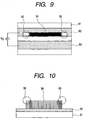
- a quartz substrate was used as the substrate 1 and fully cleaned. After that, Ti and Pt as materials of the gate electrode 2 and the cathode electrode 3 were successively deposited by a sputtering method at thicknesses of 5 nm and 30 nm, respectively, thereby forming a Ti layer and a Pt layer.
- a resist pattern was formed using a positive photoresist by a general photolithography process. Then, the Pt layer and the Ti layer were dry-etched by an Ar gas using the photoresist as a mask to form the gate electrode 2 and the cathode electrode 3 (Fig. 8A).
- the substrate temperature was kept at 300°C, and TiN was deposited at a thickness of 500 nm by a reactive sputtering method of sputtering Ti using an etching gas prepared by mixing nitrogen in Ar, thereby forming a TiN layer as the conductive layer 4.
- the substrate was sufficiently cooled to a room temperature, and then Pd was deposited by an amount enough to form an island shape by a sputtering method, thereby forming an island-shaped Pd layer 81 (Fig. 8B).
- a resist pattern was formed using a positive photoresist by a photolithography process (Fig. 8C). Then, the island-shaped Pd layer 81 and the TiN layer 4 were dry-etched by a CF 4 gas using the patterned photoresist 82 as a mask, thereby forming a metallic catalyst 81 (island-shaped Pd layer) with a desired pattern on the cathode electrode 2 (Fig 8D).
- the electron-emitting film 5 was composed of a large number of carbon fibers (electron-emitting materials) which are fibrously extended while being partially bent. A diameter of each of the carbon fibers was the order of 5 nm to 250 nm. A film thickness of the electron-emitting film 5 was the order of several ⁇ m. Electron microscope observation and Raman spectroscopic analysis were performed on the carbon fibers. As a result, it was observed that the graphite nanofiber is formed.
- the graphite nanofiber is used for the electron-emitting film 5.
- a film containing a carbon fiber the same operation is obtained.
- a carbon nanotube, an amorphous carbon fiber, a diamond fiber, or the like can be used as the carbon fiber.
- a threshold (voltage) required for election emission from the electron-emitting film 5, which is dependent on a potential of the gate electrode 3, becomes lower in the vicinity of the region of the electron-emitting film 5 in which the space between the cathode electrode 2 and the gate electrode 3 is wide.
- the edge of the cathode electrode 2 may be formed in a plurality of concave and convex shapes when it is viewed from the gate electrode 3 side. When such shapes are used, the electron-emitting region can be divided into a plurality of regions.
- a concave portion of the edge of the cathode electrode may be an elliptical concave shape.
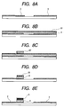
- Fig. 3 shows the electron-emitting device according to Example 2 when it is viewed from above the base surface.
- the electron-emitting device according to this example can be manufactured by the same method as for the electron-emitting device described in Example 1.
- the same references are provided to the same members as in Example 1.
- the space between the gate electrode 3 and the cathode electrode 2 is constant.
- the electron-emitting film 5 was elliptically patterned and the substantially two end portions A and B exist in a direction along a gap between the gate electrode 3 and the cathode electrode 2.
- the distance between the end of the cathode electrode 2 and the electron-emitting film 5 is relatively large in each of the end portions A and B.
- the end of the cathode electrode 2 is close to the end of the electron-emitting film 5.
- an area of a portion of the cathode electrode 2 between each of the two end portions of the electron-emitting film 5 and the gate electrode 3 is larger than an area of a portion of the cathode electrode 2 between the region located between the two end portions of the electron-emitting film 5 and the gate electrode 3.
- electrons can be selectively emitted from the region between the two end portions of the electron-emitting film 5, where the area of the portion of the cathode electrode 2 between the electron-emitting film 5 and the gate electrode 3 is smaller.
- the electron emission from the vicinities of the two end portions can be suppressed.
- Fig. 4 shows the electron-emitting device according to Example 3 when it is viewed from above the base surface.
- the electron-emitting device according to this example can be manufactured by the same method as for the electron-emitting device described in Example 1.
- the same references are provided to the same members as in Example 1.
- the electron-emitting film 5 was patterned in a strip shape with a predetermined width. Therefore, the two end portions A and B exist in the longitudinal direction of the electron-emitting film 5.
- the cathode electrode 2 protrudes more to the gate electrode 3 side in areas between each of the two end portions A and B of the electron-emitting film 5 and the gate electrode 3, as compared with an area between the region located between the two end portions of the electron-emitting film 5 and the gate electrode 3.
- the space between the gate electrode 3 and the cathode electrode 2 is not constant but is wider in the region between the two end portions A and B of the electron-emitting film 5. That is, the end of the cathode electrode 2 is closer to the electron-emitting film 5 in the region between the two end portions, as compared with the vicinities of the end portions.
- the electron emission from the vicinities of the two end portions of the electron-emitting film 5 in which the cathode electrode 2 protrudes more to the gate electrode 3 side can be suppressed, and electrons can be selectively emitted from the region between the two end portions.
- Fig. 6 shows the electron-emitting device according to Example 4 when it is viewed from above the base surface.
- the electron-emitting device according to this example can be manufactured by the same method as for the electron-emitting device described in Example 1.
- the same references are provided to the same members as in Example 1.
- the electron-emitting film 5 was patterned in a rectangular shape on the cathode electrode 2 in the plane substantially parallel to the base surface.
- the electron-emitting film 5 has the two end portions A and B in a direction substantially perpendicular to the direction along which the cathode electrode 2 and the gate electrode 3 are opposed to each other.
- the gate electrode 3 was formed such that a distance therefrom to the region located between the two end portions of the electron-emitting film 5 becomes shorter than distances up to the two end portions of the electron-emitting film 5.
- the electric field strength in the region in which the distance between the gate electrode 3 and the electron-emitting film 5 is shorter becomes higher than the electric field strength in other regions.
- the present invention includes an electron source in which a plurality of electron-emitting devices as described above are formed, and an image forming apparatus which is composed of a combination of the electron source and a light emitting member made of a phosphor or the like.
- the electron-emitting device including the electron-emitting region having a small electron-emitting distribution can be provided, and the non-uniformity in electron-emitting characteristics between the electron-emitting devices can be reduced. Further, when an electron source in which the plurality of electron-emitting devices according to the present invention are arranged, an image forming apparatus capable of uniformly displaying an image having a preferable quality on a large area can be realized.
- the electron-emitting device includes: a cathode electrode and a gate electrode, which are formed on a base surface and opposed to each other with a space therebetween; and an electron-emitting film which is located on the cathode electrode, and in the electron-emitting device, the electron-emitting film has two end portions (A and B) in a plane substantially parallel to the base surface in a direction substantially perpendicular to a direction along which the cathode electrode and the gate electrode are opposed to each other, and a structure is used in which electric field strengths applied between each of the two end portions (A and B) of the electron-emitting film and the gate electrode are made weaker than an electric field strength applied between a region between the two end portions (A and B) of the electron-emitting film and the gate electrode at a time
Landscapes
- Engineering & Computer Science (AREA)
- Chemical & Material Sciences (AREA)
- Nanotechnology (AREA)
- Theoretical Computer Science (AREA)
- Physics & Mathematics (AREA)
- Crystallography & Structural Chemistry (AREA)
- Mathematical Physics (AREA)
- General Engineering & Computer Science (AREA)
- Mechanical Engineering (AREA)
- Civil Engineering (AREA)
- Structural Engineering (AREA)
- Cold Cathode And The Manufacture (AREA)
- Cathode-Ray Tubes And Fluorescent Screens For Display (AREA)
- Electrodes For Cathode-Ray Tubes (AREA)
Abstract
Description
Claims (11)
- An electron-emitting device, characterized in that:the device comprises: a cathode electrode and a gate electrode, which are formed on a surface of a substrate and opposed to each other with a space therebetween; anda film containing an electron-emitting material, which is located on the cathode electrode, and thatthe film containing the electron-emitting material has two end portions in a plane substantially parallel to the surface of the substrate in a direction substantially perpendicular to a direction along which the cathode electrode and the gate electrode are opposed to each other, anda structure is used in which electric field strengths applied between each of the two end portions of the film containing the electron-emitting material and the gate electrode are made weaker than an electric field strength applied between a region between the two end portions of the film containing the electron-emitting material and the gate electrode at a time of driving.
- An electron-emitting device, characterized in that:the device comprises: a cathode electrode and a gate electrode, which are formed on a surface of a substrate and opposed to each other with a space therebetween; anda film containing an electron-emitting material, which is located on the cathode electrode, and thatthe film containing the electron-emitting material has two end portions in a plane substantially parallel to the surface of the substrate in a direction substantially perpendicular to a direction along which the cathode electrode and the gate electrode are opposed to each other, andan area of a portion of the cathode electrode between each of the two end portions of the film containing the electron-emitting material and the gate electrode in the plane substantially parallel to the surface of the substrate is larger than an area of a portion of the cathode electrode between a region located between the two end portions of the film containing the electron-emitting material and the gate electrode.
- An electron-emitting device, characterized in that:the device comprises: a cathode electrode and a gate electrode, which are formed on a surface of a substrate and opposed to each other with a space therebetween; anda film containing an electron-emitting material, which is located on the cathode electrode, and thatthe film containing the electron-emitting material has two end portions in a plane substantially parallel to the surface of the substrate in a direction substantially perpendicular to a direction along which the cathode electrode and the gate electrode are opposed to each other, andthe cathode electrode has protruding portions in areas between each of the two end portions of the film containing the electron-emitting material and the gate electrode in a plane substantially parallel to the surface of the substrate, the protruding portions protruding more to the gate electrode side as compared with an area between a region located between the two end portions of the film containing the electron-emitting material and the gate electrode.
- An electron-emitting device, characterized in that:the device comprises: a cathode electrode and a gate electrode, which are formed on a surface of a substrate and opposed to each other with a space therebetween; anda film containing an electron-emitting material, which is located on the cathode electrode, and thatthe film containing the electron-emitting material has two end portions in a plane substantially parallel to the surface of the substrate in a direction substantially perpendicular to a direction along which the cathode electrode and the gate electrode are opposed to each other, andthe gate electrode has a shape in which a distance therefrom to a region located between the two end portions of the film containing the electron-emitting material is shorter than a distance therefrom to each of the two end portions of the film containing the electron-emitting material.
- An electron-emitting device, characterized in that:the device comprises: a cathode electrode and a gate electrode, which are formed on a surface of a substrate and opposed to each other with a space therebetween; anda film containing an electron-emitting material, which is located on the cathode electrode, and thatthe film containing the electron-emitting material has two end portions in a plane substantially parallel to the surface of the substrate in a direction substantially perpendicular to a direction along which the cathode electrode and the gate electrode are opposed to each other, anda distance from a center line between the cathode electrode and the gate electrode to a region located between the two end portions of the film containing the electron-emitting material is shorter than a distance from the center line to each of the two end portions of the film containing the electron-emitting material.
- An electron-emitting device according to any one of claims 1 to 5, characterized in that the film containing the electron-emitting material comprises a plurality of fibrous conductive materials.
- An electron-emitting device according to any one of claims 1 to 5, characterized in that the film containing the electron-emitting material contains mainly carbon.
- An electron-emitting device according to any one of claims 1 to 5, characterized in that the film containing the electron-emitting material comprises a plurality of carbon fibers.
- An electron-emitting device according to claim 8, characterized in that each of the plurality of carbon fibers includes at least one of a carbon nanotube, a graphite nanofiber, an amorphous carbon fiber, and a diamond fiber.
- An electron source, characterized by comprising:a plurality of electron-emitting devices, each of which is constructed according to any one of claims 1 to 9.
- An image display apparatus, characterized by comprising:an electron source constructed according to claim 10; anda light emitting member.
Applications Claiming Priority (2)
| Application Number | Priority Date | Filing Date | Title |
|---|---|---|---|
| JP2003061255A JP3703459B2 (en) | 2003-03-07 | 2003-03-07 | Electron emitter, electron source, image display device |
| JP2003061255 | 2003-03-07 |
Publications (3)
| Publication Number | Publication Date |
|---|---|
| EP1455376A2 true EP1455376A2 (en) | 2004-09-08 |
| EP1455376A3 EP1455376A3 (en) | 2005-01-19 |
| EP1455376B1 EP1455376B1 (en) | 2007-09-12 |
Family
ID=32821228
Family Applications (1)
| Application Number | Title | Priority Date | Filing Date |
|---|---|---|---|
| EP04005148A Expired - Lifetime EP1455376B1 (en) | 2003-03-07 | 2004-03-04 | Electron-emitting device, electron source, and image display apparatus |
Country Status (6)
| Country | Link |
|---|---|
| US (1) | US7138759B2 (en) |
| EP (1) | EP1455376B1 (en) |
| JP (1) | JP3703459B2 (en) |
| KR (1) | KR100586580B1 (en) |
| CN (1) | CN1305092C (en) |
| DE (1) | DE602004008812T2 (en) |
Families Citing this family (8)
| Publication number | Priority date | Publication date | Assignee | Title |
|---|---|---|---|---|
| JP4324078B2 (en) * | 2003-12-18 | 2009-09-02 | キヤノン株式会社 | Carbon-containing fiber, substrate using carbon-containing fiber, electron-emitting device, electron source using the electron-emitting device, display panel using the electron source, and information display / reproduction device using the display panel, And production methods thereof |
| KR101013438B1 (en) * | 2004-02-09 | 2011-02-14 | 삼성에스디아이 주식회사 | Field emission device and backlight device having same |
| JP3935479B2 (en) * | 2004-06-23 | 2007-06-20 | キヤノン株式会社 | Carbon fiber manufacturing method, electron-emitting device manufacturing method using the same, electronic device manufacturing method, image display device manufacturing method, and information display / reproducing apparatus using the image display device |
| JP4596878B2 (en) | 2004-10-14 | 2010-12-15 | キヤノン株式会社 | Structure, electron-emitting device, secondary battery, electron source, image display device, information display / reproduction device, and manufacturing method thereof |
| US7701128B2 (en) * | 2005-02-04 | 2010-04-20 | Industrial Technology Research Institute | Planar light unit using field emitters and method for fabricating the same |
| TWI435358B (en) * | 2005-08-10 | 2014-04-21 | Pureron Japan Co Ltd | A carbon film having a shape suitable for the emission of electric field, a carbon film structure, and an electron emitter |
| WO2007114655A1 (en) * | 2006-04-05 | 2007-10-11 | Industry Academic Cooperation Foundation Of Kyunghee University | Field emission display and manufacturing method of the same having selective array of electron emission source |
| US9415095B2 (en) * | 2014-08-02 | 2016-08-16 | Gatan, Inc. | Method for image outlier removal for transmission electron microscope cameras |
Family Cites Families (20)
| Publication number | Priority date | Publication date | Assignee | Title |
|---|---|---|---|---|
| US4728851A (en) | 1982-01-08 | 1988-03-01 | Ford Motor Company | Field emitter device with gated memory |
| US4904895A (en) | 1987-05-06 | 1990-02-27 | Canon Kabushiki Kaisha | Electron emission device |
| US5382867A (en) * | 1991-10-02 | 1995-01-17 | Sharp Kabushiki Kaisha | Field-emission type electronic device |
| JP3156903B2 (en) | 1994-09-29 | 2001-04-16 | シャープ株式会社 | Field emission type electron source |
| JP3423511B2 (en) * | 1994-12-14 | 2003-07-07 | キヤノン株式会社 | Image forming apparatus and getter material activation method |
| JPH09190783A (en) * | 1996-01-11 | 1997-07-22 | Canon Inc | Image forming device |
| US6259422B1 (en) * | 1997-08-06 | 2001-07-10 | Canon Kabushiki Kaisha | Method for producing image-forming apparatus |
| US6648711B1 (en) * | 1999-06-16 | 2003-11-18 | Iljin Nanotech Co., Ltd. | Field emitter having carbon nanotube film, method of fabricating the same, and field emission display device using the field emitter |
| JP3769149B2 (en) | 1999-08-03 | 2006-04-19 | 株式会社リコー | Electron-emitting device, manufacturing method thereof, and image forming apparatus using the electron-emitting device |
| US20020036452A1 (en) * | 1999-12-21 | 2002-03-28 | Masakazu Muroyama | Electron emission device, cold cathode field emission device and method for the production thereof, and cold cathode field emission display and method for the production thereof |
| JP2002025477A (en) | 2000-07-07 | 2002-01-25 | Ise Electronics Corp | Surface display and its manufacturing method |
| JP3639809B2 (en) | 2000-09-01 | 2005-04-20 | キヤノン株式会社 | ELECTRON EMITTING ELEMENT, ELECTRON EMITTING DEVICE, LIGHT EMITTING DEVICE, AND IMAGE DISPLAY DEVICE |
| JP3639808B2 (en) * | 2000-09-01 | 2005-04-20 | キヤノン株式会社 | Electron emitting device, electron source, image forming apparatus, and method of manufacturing electron emitting device |
| JP3610325B2 (en) * | 2000-09-01 | 2005-01-12 | キヤノン株式会社 | Electron emitting device, electron source, and method of manufacturing image forming apparatus |
| JP3737696B2 (en) | 2000-11-17 | 2006-01-18 | 株式会社東芝 | Method for manufacturing horizontal field emission cold cathode device |
| JP2003068189A (en) * | 2001-03-14 | 2003-03-07 | Futaba Corp | Manufacturing method of fluorescent character display tube and fluorescent character display tube |
| JP4593816B2 (en) | 2001-03-27 | 2010-12-08 | キヤノン株式会社 | Electron emitting device, image forming apparatus, and method of manufacturing electron emitting device |
| JP3768908B2 (en) * | 2001-03-27 | 2006-04-19 | キヤノン株式会社 | Electron emitting device, electron source, image forming apparatus |
| JP3647436B2 (en) | 2001-12-25 | 2005-05-11 | キヤノン株式会社 | Electron-emitting device, electron source, image display device, and method for manufacturing electron-emitting device |
| JP3902964B2 (en) | 2002-02-28 | 2007-04-11 | キヤノン株式会社 | Manufacturing method of electron source |
-
2003
- 2003-03-07 JP JP2003061255A patent/JP3703459B2/en not_active Expired - Fee Related
-
2004
- 2004-03-02 US US10/789,995 patent/US7138759B2/en not_active Expired - Fee Related
- 2004-03-04 EP EP04005148A patent/EP1455376B1/en not_active Expired - Lifetime
- 2004-03-04 DE DE602004008812T patent/DE602004008812T2/en not_active Expired - Lifetime
- 2004-03-05 CN CNB2004100077902A patent/CN1305092C/en not_active Expired - Fee Related
- 2004-03-06 KR KR1020040015275A patent/KR100586580B1/en not_active Expired - Fee Related
Also Published As
| Publication number | Publication date |
|---|---|
| CN1305092C (en) | 2007-03-14 |
| EP1455376B1 (en) | 2007-09-12 |
| DE602004008812T2 (en) | 2008-06-05 |
| DE602004008812D1 (en) | 2007-10-25 |
| EP1455376A3 (en) | 2005-01-19 |
| CN1527340A (en) | 2004-09-08 |
| US20040183428A1 (en) | 2004-09-23 |
| KR20040081028A (en) | 2004-09-20 |
| JP3703459B2 (en) | 2005-10-05 |
| US7138759B2 (en) | 2006-11-21 |
| KR100586580B1 (en) | 2006-06-07 |
| JP2004273232A (en) | 2004-09-30 |
Similar Documents
| Publication | Publication Date | Title |
|---|---|---|
| EP1511058B1 (en) | Carbon-nano tube structure, method of manufacturing the same, and field emitter and display device each adopting the same | |
| JP3768908B2 (en) | Electron emitting device, electron source, image forming apparatus | |
| US6780075B2 (en) | Method of fabricating nano-tube, method of manufacturing field-emission type cold cathode, and method of manufacturing display device | |
| US6853126B2 (en) | Electron-emitting device, electron source, image forming apparatus, and electron-emitting apparatus | |
| US7687981B2 (en) | Method for controlled density growth of carbon nanotubes | |
| JP3497740B2 (en) | Method for producing carbon nanotube and method for producing field emission cold cathode device | |
| US6975288B2 (en) | Method of driving image-forming apparatus and apparatus thereof | |
| US20090098671A1 (en) | Nanotube assembly including protective layer and method for making the same | |
| US7115013B2 (en) | Method for making a carbon nanotube-based field emission display | |
| US7811641B2 (en) | Method of forming carbon nanotubes, field emission display device having carbon nanotubes formed through the method, and method of manufacturing field emission display device | |
| US20090325452A1 (en) | Cathode substrate having cathode electrode layer, insulator layer, and gate electrode layer formed thereon | |
| US20030059968A1 (en) | Method of producing field emission display | |
| US7465210B2 (en) | Method of fabricating carbide and nitride nano electron emitters | |
| JP2006224296A (en) | Carbon nanotube structure and method for manufacturing the same, field emission device using carbon nanotube structure, and method for manufacturing the same | |
| US7138759B2 (en) | Electron-emitting device, electron source, and image display apparatus | |
| US20050067936A1 (en) | Self-aligned gated carbon nanotube field emitter structures and associated methods of fabrication | |
| JP3502804B2 (en) | Method for growing carbon nanotubes and method for manufacturing electron gun and probe using the same | |
| KR100668332B1 (en) | Method for manufacturing a device with carbide and nitride nanoelectronic emitters | |
| JP3897794B2 (en) | Method for manufacturing electron-emitting device, electron source, and image forming apparatus | |
| US20080030122A1 (en) | Electron emitting element, manufacturing method for electron emitting element, and display device having electron emitting element | |
| JP2005048305A (en) | Carbon fiber manufacturing method, and electron emitting device, electron source, and image display device manufacturing method using the same | |
| JP2006134724A (en) | Field emitter array and manufacturing method thereof | |
| KR20020005794A (en) | Carbon nano tube field emission element and apparatus using it | |
| KR20020060422A (en) | FED using carbon nanotube and manufacturing method thereof | |
| JP2005032449A (en) | Electron emission device and image display device |
Legal Events
| Date | Code | Title | Description |
|---|---|---|---|
| PUAI | Public reference made under article 153(3) epc to a published international application that has entered the european phase |
Free format text: ORIGINAL CODE: 0009012 |
|
| AK | Designated contracting states |
Kind code of ref document: A2 Designated state(s): AT BE BG CH CY CZ DE DK EE ES FI FR GB GR HU IE IT LI LU MC NL PL PT RO SE SI SK TR |
|
| AX | Request for extension of the european patent |
Extension state: AL LT LV MK |
|
| PUAL | Search report despatched |
Free format text: ORIGINAL CODE: 0009013 |
|
| AK | Designated contracting states |
Kind code of ref document: A3 Designated state(s): AT BE BG CH CY CZ DE DK EE ES FI FR GB GR HU IE IT LI LU MC NL PL PT RO SE SI SK TR |
|
| AX | Request for extension of the european patent |
Extension state: AL LT LV MK |
|
| 17P | Request for examination filed |
Effective date: 20050718 |
|
| AKX | Designation fees paid |
Designated state(s): DE FR GB IT NL |
|
| GRAP | Despatch of communication of intention to grant a patent |
Free format text: ORIGINAL CODE: EPIDOSNIGR1 |
|
| GRAS | Grant fee paid |
Free format text: ORIGINAL CODE: EPIDOSNIGR3 |
|
| GRAA | (expected) grant |
Free format text: ORIGINAL CODE: 0009210 |
|
| AK | Designated contracting states |
Kind code of ref document: B1 Designated state(s): DE FR GB IT NL |
|
| REG | Reference to a national code |
Ref country code: GB Ref legal event code: FG4D |
|
| REF | Corresponds to: |
Ref document number: 602004008812 Country of ref document: DE Date of ref document: 20071025 Kind code of ref document: P |
|
| ET | Fr: translation filed | ||
| PLBE | No opposition filed within time limit |
Free format text: ORIGINAL CODE: 0009261 |
|
| STAA | Information on the status of an ep patent application or granted ep patent |
Free format text: STATUS: NO OPPOSITION FILED WITHIN TIME LIMIT |
|
| 26N | No opposition filed |
Effective date: 20080613 |
|
| PGFP | Annual fee paid to national office [announced via postgrant information from national office to epo] |
Ref country code: DE Payment date: 20120331 Year of fee payment: 9 |
|
| PGFP | Annual fee paid to national office [announced via postgrant information from national office to epo] |
Ref country code: IT Payment date: 20120312 Year of fee payment: 9 Ref country code: GB Payment date: 20120223 Year of fee payment: 9 |
|
| PGFP | Annual fee paid to national office [announced via postgrant information from national office to epo] |
Ref country code: NL Payment date: 20120322 Year of fee payment: 9 |
|
| PGFP | Annual fee paid to national office [announced via postgrant information from national office to epo] |
Ref country code: FR Payment date: 20120413 Year of fee payment: 9 |
|
| REG | Reference to a national code |
Ref country code: NL Ref legal event code: V1 Effective date: 20131001 |
|
| GBPC | Gb: european patent ceased through non-payment of renewal fee |
Effective date: 20130304 |
|
| REG | Reference to a national code |
Ref country code: FR Ref legal event code: ST Effective date: 20131129 |
|
| REG | Reference to a national code |
Ref country code: DE Ref legal event code: R119 Ref document number: 602004008812 Country of ref document: DE Effective date: 20131001 |
|
| PG25 | Lapsed in a contracting state [announced via postgrant information from national office to epo] |
Ref country code: DE Free format text: LAPSE BECAUSE OF NON-PAYMENT OF DUE FEES Effective date: 20131001 Ref country code: FR Free format text: LAPSE BECAUSE OF NON-PAYMENT OF DUE FEES Effective date: 20130402 Ref country code: GB Free format text: LAPSE BECAUSE OF NON-PAYMENT OF DUE FEES Effective date: 20130304 |
|
| PG25 | Lapsed in a contracting state [announced via postgrant information from national office to epo] |
Ref country code: NL Free format text: LAPSE BECAUSE OF NON-PAYMENT OF DUE FEES Effective date: 20131001 Ref country code: IT Free format text: LAPSE BECAUSE OF NON-PAYMENT OF DUE FEES Effective date: 20130304 |