EP1453346B1 - Configurable electrical transceiver in a small form factor pluggable module realising coded interfaces - Google Patents
Configurable electrical transceiver in a small form factor pluggable module realising coded interfaces Download PDFInfo
- Publication number
- EP1453346B1 EP1453346B1 EP20030425123 EP03425123A EP1453346B1 EP 1453346 B1 EP1453346 B1 EP 1453346B1 EP 20030425123 EP20030425123 EP 20030425123 EP 03425123 A EP03425123 A EP 03425123A EP 1453346 B1 EP1453346 B1 EP 1453346B1
- Authority
- EP
- European Patent Office
- Prior art keywords
- module
- receiving
- electrical
- interface
- host
- Prior art date
- Legal status (The legal status is an assumption and is not a legal conclusion. Google has not performed a legal analysis and makes no representation as to the accuracy of the status listed.)
- Expired - Fee Related
Links
Images


Classifications
-
- H—ELECTRICITY
- H04—ELECTRIC COMMUNICATION TECHNIQUE
- H04J—MULTIPLEX COMMUNICATION
- H04J3/00—Time-division multiplex systems
- H04J3/02—Details
- H04J3/04—Distributors combined with modulators or demodulators
-
- H—ELECTRICITY
- H04—ELECTRIC COMMUNICATION TECHNIQUE
- H04J—MULTIPLEX COMMUNICATION
- H04J3/00—Time-division multiplex systems
- H04J3/16—Time-division multiplex systems in which the time allocation to individual channels within a transmission cycle is variable, e.g. to accommodate varying complexity of signals, to vary number of channels transmitted
- H04J3/1605—Fixed allocated frame structures
- H04J3/1611—Synchronous digital hierarchy [SDH] or SONET
-
- H—ELECTRICITY
- H04—ELECTRIC COMMUNICATION TECHNIQUE
- H04J—MULTIPLEX COMMUNICATION
- H04J3/00—Time-division multiplex systems
- H04J3/16—Time-division multiplex systems in which the time allocation to individual channels within a transmission cycle is variable, e.g. to accommodate varying complexity of signals, to vary number of channels transmitted
- H04J3/1605—Fixed allocated frame structures
- H04J3/1623—Plesiochronous digital hierarchy [PDH]
-
- H—ELECTRICITY
- H04—ELECTRIC COMMUNICATION TECHNIQUE
- H04Q—SELECTING
- H04Q11/00—Selecting arrangements for multiplex systems
- H04Q11/04—Selecting arrangements for multiplex systems for time-division multiplexing
- H04Q11/0421—Circuit arrangements therefor
-
- H—ELECTRICITY
- H04—ELECTRIC COMMUNICATION TECHNIQUE
- H04Q—SELECTING
- H04Q2213/00—Indexing scheme relating to selecting arrangements in general and for multiplex systems
- H04Q2213/13003—Constructional details of switching devices
-
- H—ELECTRICITY
- H04—ELECTRIC COMMUNICATION TECHNIQUE
- H04Q—SELECTING
- H04Q2213/00—Indexing scheme relating to selecting arrangements in general and for multiplex systems
- H04Q2213/1301—Optical transmission, optical switches
-
- H—ELECTRICITY
- H04—ELECTRIC COMMUNICATION TECHNIQUE
- H04Q—SELECTING
- H04Q2213/00—Indexing scheme relating to selecting arrangements in general and for multiplex systems
- H04Q2213/13109—Initializing, personal profile
-
- H—ELECTRICITY
- H04—ELECTRIC COMMUNICATION TECHNIQUE
- H04Q—SELECTING
- H04Q2213/00—Indexing scheme relating to selecting arrangements in general and for multiplex systems
- H04Q2213/13214—Clock signals
-
- H—ELECTRICITY
- H04—ELECTRIC COMMUNICATION TECHNIQUE
- H04Q—SELECTING
- H04Q2213/00—Indexing scheme relating to selecting arrangements in general and for multiplex systems
- H04Q2213/13367—Hierarchical multiplexing, add-drop multiplexing
Definitions
- the present invention relates to an electrical transceiver which realises both of the SDH-STM1/Sonet-STS3 and PDH-E4 ITU-T G.703 CMI (Code Mark Inversion) coded interface.
- the claimed electrical transceiver is realised in a Small Form Factor Pluggable Module and can be programmed as STM1/STS3 or E4-PDH by simply applying the right configuration on the Serial Identification interface.
- the STM1/STS3 interfaces are specified in two different versions according to the nature of the signal adopted for the transmission.
- the signal format can, in fact, be either electrical or optical :
- SFP Small Form Factor Pluggable
- GBIC gigabit interface converter
- SOC optical converter
- an electrical module based on the Small Form Factor Pluggable (SFP) standard, that allows the implementation on a single card, of the STM1/STS3 or PDH-E4 transmission interfaces, in the electrical as well as in the optical format, is considered very useful.
- SFP Small Form Factor Pluggable
- E4-PDH variant of the card still required for interfacing installed legacy equipment, will not risk to be thrown away when this legacy world will disappear, because it can easily be reused as electrical STM1/STS3 (by simple SW modification), or reused as optical STM1/STS3 interface (by substitution of the pluggable module).
- a transceiver module configurable so as to act as an SDH STM1 interface or PDH E4 interface is disclosed in the paper "A single Chip 155 Mbps/140 Mbps SDH/PDH Transceiver", J. Guinea et al., Proceedings of the IEEE 2000 Custom Integrated Ciruit Conference, Orlando, FI, USA, 21 - 24 May 2000, pp. 315 - 318, upon which the preamble of claim 1 is based.
- This prior art transceiver includes: printed circuit means having a first and second end; coaxial connecting means mounted at the first end of said printed circuit means; multipad electrical connecting means mounted at the second end of said printed circuit means; receiving/transmitting means mounted on said printed circuit means and connected to said coaxial connecting means and to said multi-pad electrical means; and timing means connected to said receiving/transmitting means and providing timing signals required by the CMI decoder/encoder.
- the prior art transceiver needs an external clock signal for generating the timing signals necessary for the operation of the transmitting means and thus it is not compatible with the SFP MSA, as an SFP MSA compliant host board has no pin for outputting such a clock signal.
- the present invention provides a configurable electrical transceiver having the features claimed in the main claim. More specifically, according to the present invention, an intelligent processing unit (ASIC) has been developed able to handle signals for the STM1/STS3 as well as the PDH /E4 transmission interfaces.
- ASIC intelligent processing unit
- an host circuit board which can be used for all the following applications:
- the present invention concerns a Configurable Electrical Small form Factor Pluggable Module (CESFP) that is an electrical transceiver, electrically and mechanically compatible with the optical SFP module, realising in a very small space the SDH-STM1/Sonet-STS3 and PDH-E4 ITU-T G.703 CMI (Code Mark Inversion) coded interface.
- CESFP Configurable Electrical Small form Factor Pluggable Module
- the CESFP module can be programmed as STM1/STS3 or E4-PDH by simply applying the right configuration on the Serial Identification interface (pins MOD-DEF 1 and MOD-DEF 2).
- the CESFP module is packaged in a metal housing which slides in a metallic booth (receptacle plus electrical connector) placed on the host.
- the receptacle (cage) and the connector pin out are compliant to the Small Form-factor Pluggable (SFP) Transceiver MultiSource Agreement (MSA) September 2000.
- SFP Small Form-factor Pluggable
- the transceiver consists of a printed circuit board having as input/output physical interfaces two different types of connectors:
- the main functions implemented on the printed circuit board are:
- the Figure 1 provides the electrical block diagram as described in the following sections.
- the CMI coded line signal is received via a small coax connector.
- the CMI is a 1B2B non-return-to-zero code where each bit of information is coded into two transmission bits. A binary “0” is coded to "01” and a binary “1” is alternately coded with "00" or "11", thus there is at least one transition during every bit period.
- a cable equalisation circuit together with an amplifier provide the recover of the original signal shape and amplitude, deteriorated by the cable attenuation and generate the appropriate signal to drive the CMI decoder.
- the CMI decoder accepts a differential data input and with the support of an internal reference clock returns an NRZ coded data stream, which is routed via two coupling capacitors to the -connector- pads (pins RD+,RD-).
- the Loss of signal (LOS) circuit monitors the power level of the incoming signal and generates an alarm when the received signal is below a pre-defined threshold.
- the transmit section consists of a NRZ/CMI encoder and a transmit buffer.
- the differential NRZ signal is received from the pad connector (pin TD+,TD-).
- the NRZ data signal, AC-coupled, is routed to the coding circuit and converted into a CMI-coded stream with the support of an internal reference clock.
- the transmit buffer provides an output signal capable of driving a 75 Ohm transmission line compliant with ITU-G.703.
- the transmit CMI coded signal is outputted on a coax cable connector.
- the NRZ output/input high-speed balanced-signals are ac-coupled.
- the coupling capacitors are large enough to let the SDH test pattern signal pass through without significant distortion or performance penalty.
- an on board VCO provides the clock reference required by the encoder/decoder to perform the CMI/NRZ and NRZ/CMI conversions.
- the device can be configured via a2-wire clocked Serial Interface and set for the STS3/STM1 or PDH-E4 application.
- This operation can be done by the host card controller when the module is already in field, and after it has been recognised as an electrical STM1(STS3)/PDH transceiver.
- This information being stored in the memory (EEPROM) placed on the module, at the moment of its assembling.
- the 2-wire clocked serial interface (I2Cbus) provides access to an internal EEPROM memory where sophisticated identification information (figure 3) have previously been stored in an MSA compliant fashion:
- the serial interface consists of :
- a ground on the- MOD-DEF 0- pin indicates that the module is present.
- the configurable electrical transceiver module (CESFP) is realised in a Small Form-factor Pluggable Module (SFP) and the receptacle (cage) and the connector pin out are compliant to a Multi-Source Agreement SFP optical transceiver.
- SFP Small Form-factor Pluggable Module
- the receptacle (cage) and the connector pin out are compliant to a Multi-Source Agreement SFP optical transceiver.
- the CESFP module is packaged in a metal housing which slides in a metallic booth (receptacle plus electrical connector) placed on the host.
- the module includes a cover, a printed circuit board, a base and a couple of small coax cable connectors.
- the printed circuit board (100) have a first end and a second end.
- the first end of the board is connected to the couple of small coax cable connectors (101,102), the first one connector (101) providing the CMI code input from external coaxial cable, the second one connector (102) providing the CMI code output to the external coaxial cable.
- the printed circuit board have a 20-pad slide-in type connector that connects the printed circuit board (100) to a female electrical connector (201) placed on the host board (200).
- the circuit board (100) exchanges to/from the host board(200), signals, alarms, power and ground according to the pin-out provided in the table reported in figure 4.
- the circuit board(100) have a receive section (110) that receives the line signal, in the CMI code format, through the connector (101).
- a cable equalisation circuit (111) together with an amplifier (112) provides to recover the original signal shape and amplitude, deteriorated by the cable attenuation and generates the appropriate signal to drive the CMI decoder (113).
- the CMI decoder (113) accepts a differential data input and with the support of an internal reference clock, belonging to the programmable internal timing reference circuit (120), returns an NRZ coded data stream (RD data out), which is routed via two coupling capacitors to the connector (201) of the host board (200) depicted in figure 2 .
- the Loss of signal (LOS) circuit monitors the power level of the incoming signal and generates an alarm when the received signal is below a pre-defined threshold.
- the transmitting section (130) receives a differential NRZ signal (RD data in) from the connector (201) of the host board (200).
- the NRZ data signal (RD data in), AC-coupled, is routed to the encoding circuit (131) and converted into a CMI-coded stream with the support of an internal reference clock belonging to the programmable internal timing reference circuit (120).
- the transmit buffer (132) receive the CMI-coded stream and provides an output signal capable of driving a 75 Ohm transmission line compliant with ITU-G.703.
- the CMI coded signal is transmitted by the coax cable connector (102).
- an on board VCO provides the clock reference required by the encoder/decoder to perform the CMI/NRZ and NRZ/CMI conversions.
- the host card controller (202) can configure, via a 2-wire clocked Serial Interface, the programmable internal timing reference circuit (120), setting it for the STS3/STM1 or PDH-E4 application.
- serial interface consists of :
- the host card controller (202) can recognise, via the MOD-Def0 pin, that the module is present and, via the MOD-Def1 and MOD-Def2 pins of the 2-wire clocked serial interface ( I2Cbus), can access the internal EEPROM memory (140) where sophisticated identification information (Table reported in Figure 3) have previously been stored in an MSA compliant fashion:
- the host controller via the same serial interface, will input the chosen configuration.
- the CMI decoder (113) and the CMI encoder (131), together with the programmable internal timing reference circuit (120), can be placed on the host board instead of inside the CESFP module, either in a discrete form or integrated within an Application Specific Integrated Circuit (ASIC).
- ASIC Application Specific Integrated Circuit
Description
- The present invention relates to an electrical transceiver which realises both of the SDH-STM1/Sonet-STS3 and PDH-E4 ITU-T G.703 CMI (Code Mark Inversion) coded interface.
- The claimed electrical transceiver is realised in a Small Form Factor Pluggable Module and can be programmed as STM1/STS3 or E4-PDH by simply applying the right configuration on the Serial Identification interface.
- This allows to adopt the same interface for both applications and to specialise it on field at the moment of its utilisation.
- In the Sonet/SDH standards, the STM1/STS3 interfaces are specified in two different versions according to the nature of the signal adopted for the transmission.
- The signal format can, in fact, be either electrical or optical :
- The electrical signal is normally used for intra station connections;
- The optical format can cover, with different implementation, the short as well as the long haul connections.
- These cards are normally multi-port; and the high degree of integration achieved today allows modularity of more than 10 interfaces/card.
- Another type of transmission interface very popular before the advent of the SDH/Sonet, and still used in the telecom world, is the 144Mbit E4 of the Plesiochronous Digital Hierarchy (PDH).
- The realisation within the transmission equipment of the two types of transmission interfaces (STM1/STS3 or PDH-E4) and two types of line card interfaces (optical or electrical), has required, until now, the implementation of distinguished units.
- The development and implementation of the many variants of transmission interfaces, translate in :
- more development effort, in HW,SW and management,
- more cost for the customer,
- more items to handle,
- more spares parts,
- The recent advent of Small Form Factor Pluggable (SFP) optical modules (see "Small Form-Factor Pluggable (SFP) Transceiver MultiSource Agreement (MSA)", 14 September 2000) has reduced some of these problems within the category of the optical interfaces.
- Several pluggable module designs and standards have been introduced in which a pluggable module plugs into a receptacle which is electronically connected to a host circuit board.
- These standards offer a generally robust design which has been well received in industry and has been used to develop gigabit interface converter (GBIC) and optical converter (SOC) and providing an interface between a computer and a data communication network such as Ethernet or Fibre Channel.
- Nevertheless, an electrical module, based on the Small Form Factor Pluggable (SFP) standard, that allows the implementation on a single card, of the STM1/STS3 or PDH-E4 transmission interfaces, in the electrical as well as in the optical format, is considered very useful.
- Until now every type of interface was implemented on a different dedicated card.
- We had :
- Many STM1/STS3 optical interface card variants (according to the transmission span, and to the wavelength used as for the ITU G.957) : I-1, S-1.1, S-1.2, L-1.1, L-1.2, L1.3
- STM1/STS3 electrical interface card
- E4 PDH electrical interface card
- Therefore, there is the need for a versatile module, configurable according to the SDH or PDH electrical standard and that allows the reusability of the same host circuit board in case of transition from electrical to optical line card interface and from Plesiochronous to Synchronous.
- This means, for instance, that the E4-PDH variant of the card, still required for interfacing installed legacy equipment, will not risk to be thrown away when this legacy world will disappear, because it can easily be reused as electrical STM1/STS3 (by simple SW modification), or reused as optical STM1/STS3 interface (by substitution of the pluggable module).
- This translates in the following advantages :
- Smaller number of items to handle for the customer
- Smaller number of spare parts to store
- The same card (in case of multi port card) can be shared between the electrical and optical interface: card number saving.
- A transceiver module configurable so as to act as an SDH STM1 interface or PDH E4 interface is disclosed in the paper "A single Chip 155 Mbps/140 Mbps SDH/PDH Transceiver", J. Guinea et al., Proceedings of the IEEE 2000 Custom Integrated Ciruit Conference, Orlando, FI, USA, 21 - 24 May 2000, pp. 315 - 318, upon which the preamble of
claim 1 is based. This prior art transceiver includes: printed circuit means having a first and second end; coaxial connecting means mounted at the first end of said printed circuit means; multipad electrical connecting means mounted at the second end of said printed circuit means; receiving/transmitting means mounted on said printed circuit means and connected to said coaxial connecting means and to said multi-pad electrical means; and timing means connected to said receiving/transmitting means and providing timing signals required by the CMI decoder/encoder. - The prior art transceiver needs an external clock signal for generating the timing signals necessary for the operation of the transmitting means and thus it is not compatible with the SFP MSA, as an SFP MSA compliant host board has no pin for outputting such a clock signal.
- The present invention provides a configurable electrical transceiver having the features claimed in the main claim. More specifically, according to the present invention, an intelligent processing unit (ASIC) has been developed able to handle signals for the STM1/STS3 as well as the PDH /E4 transmission interfaces.
- According to one aspect of the invention, by adopting such ASIC, an host circuit board has been implemented which can be used for all the following applications:
- STM1/STS3 optical;
- STM1/STS3 electrical;
- E4 PDH electrical,
- According to the above, the present invention concerns a Configurable Electrical Small form Factor Pluggable Module (CESFP) that is an electrical transceiver, electrically and mechanically compatible with the optical SFP module, realising in a very small space the SDH-STM1/Sonet-STS3 and PDH-E4 ITU-T G.703 CMI (Code Mark Inversion) coded interface.
- The CESFP module can be programmed as STM1/STS3 or E4-PDH by simply applying the right configuration on the Serial Identification interface (pins MOD-
DEF 1 and MOD-DEF 2). - This allows adopting the same interface for both applications and to specialise it on field at the moment of its utilisation.
- The CESFP module is packaged in a metal housing which slides in a metallic booth (receptacle plus electrical connector) placed on the host. The receptacle (cage) and the connector pin out are compliant to the Small Form-factor Pluggable (SFP) Transceiver MultiSource Agreement (MSA) September 2000.
- The transceiver consists of a printed circuit board having as input/output physical interfaces two different types of connectors:
- A couple of small coax cable connectors providing the line side front access.
- A 20-pad slide-in type connector that connects the module printed circuit board (signals, alarms, power and ground) to the female electrical connector placed on the host board.
- The main functions implemented on the printed circuit board are:
- Power supply distribution
- Cable Equaliser
- CMI encoder and decoder
- Alarm detectors
- AC - coupled inputs and outputs data signals
- Configurable Timing signal generation section
- Serial interface for identification and configuration
- The Figure 1 provides the electrical block diagram as described in the following sections.
In the receive section, the CMI coded line signal, is received via a small coax connector. The CMI is a 1B2B non-return-to-zero code where each bit of information is coded into two transmission bits. A binary "0" is coded to "01" and a binary "1" is alternately coded with "00" or "11", thus there is at least one transition during every bit period. A cable equalisation circuit together with an amplifier provide the recover of the original signal shape and amplitude, deteriorated by the cable attenuation and generate the appropriate signal to drive the CMI decoder. The CMI decoder accepts a differential data input and with the support of an internal reference clock returns an NRZ coded data stream, which is routed via two coupling capacitors to the -connector- pads (pins RD+,RD-). - The Loss of signal (LOS) circuit monitors the power level of the incoming signal and generates an alarm when the received signal is below a pre-defined threshold.
- The transmit section consists of a NRZ/CMI encoder and a transmit buffer.
- The differential NRZ signal is received from the pad connector (pin TD+,TD-).
- The NRZ data signal, AC-coupled, is routed to the coding circuit and converted into a CMI-coded stream with the support of an internal reference clock.
- The transmit buffer provides an output signal capable of driving a 75 Ohm transmission line compliant with ITU-G.703. The transmit CMI coded signal is outputted on a coax cable connector.
- The NRZ output/input high-speed balanced-signals are ac-coupled.
- The coupling capacitors are large enough to let the SDH test pattern signal pass through without significant distortion or performance penalty.
- In the Configurable Timing signal generation section, an on board VCO provides the clock reference required by the encoder/decoder to perform the CMI/NRZ and NRZ/CMI conversions.
- The device can be configured via a2-wire clocked Serial Interface and set for the STS3/STM1 or PDH-E4 application.
- This operation can be done by the host card controller when the module is already in field, and after it has been recognised as an electrical STM1(STS3)/PDH transceiver. This information being stored in the memory (EEPROM) placed on the module, at the moment of its assembling.
- The 2-wire clocked serial interface (I2Cbus) provides access to an internal EEPROM memory where sophisticated identification information (figure 3) have previously been stored in an MSA compliant fashion:
- CESFP's characteristics
- Module manufacturer
- Other information.
- The serial interface consists of :
- MOD-DEF 1 - the 2-wire serial interface clock signal
- MOD-DEF 2 - the 2-wire serial interface data signal A power supply section supplies the CESFP module.
- A ground on the- MOD-DEF 0- pin indicates that the module is present.
- The features of the present invention which are considered to be novel are set forth with particularity in the appended claims. The invention together with additional objects and advantages thereof maybe better understood from the following detailed description of a preferred embodiment, taken in conjunction with the accompanying drawings, in which:
- Figure 1 provides the block diagram of the CESFP module.
- Figure 2 provides the interface between the CESFP module and the host circuit board.
- Figure 3 provides the identification information of the internal EEPROM memory.
- Figure 4 provides the pin-out of the pad connector.
- The embodiment of the invention, shown in the figures wherein like referenced numerals designate identical or corresponding parts, and described below refers to the device object of the invention.
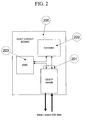
- Generally, the configurable electrical transceiver module (CESFP) is realised in a Small Form-factor Pluggable Module (SFP) and the receptacle (cage) and the connector pin out are compliant to a Multi-Source Agreement SFP optical transceiver.
- The CESFP module is packaged in a metal housing which slides in a metallic booth (receptacle plus electrical connector) placed on the host.
- The module includes a cover, a printed circuit board, a base and a couple of small coax cable connectors.
- The invention will be better understood after a discussion of related material as shown in Figure 1 that discloses the functional block diagram of the configurable electrical transceiver module (CESFP).
- The printed circuit board (100) have a first end and a second end.
- The first end of the board is connected to the couple of small coax cable connectors (101,102), the first one connector (101) providing the CMI code input from external coaxial cable, the second one connector (102) providing the CMI code output to the external coaxial cable.
- At the second end, the printed circuit board have a 20-pad slide-in type connector that connects the printed circuit board (100) to a female electrical connector (201) placed on the host board (200).
- Through the 20-pad connector, the circuit board (100) exchanges to/from the host board(200), signals, alarms, power and ground according to the pin-out provided in the table reported in figure 4.
- The circuit board(100) have a receive section (110) that receives the line signal, in the CMI code format, through the connector (101).
- A cable equalisation circuit (111) together with an amplifier (112) provides to recover the original signal shape and amplitude, deteriorated by the cable attenuation and generates the appropriate signal to drive the CMI decoder (113).
The CMI decoder (113) accepts a differential data input and with the support of an internal reference clock, belonging to the programmable internal timing reference circuit (120), returns an NRZ coded data stream (RD data out), which is routed via two coupling capacitors to the connector (201) of the host board (200) depicted in figure 2. - The Loss of signal (LOS) circuit monitors the power level of the incoming signal and generates an alarm when the received signal is below a pre-defined threshold.
- The transmitting section (130) receives a differential NRZ signal (RD data in) from the connector (201) of the host board (200).
- The NRZ data signal (RD data in), AC-coupled, is routed to the encoding circuit (131) and converted into a CMI-coded stream with the support of an internal reference clock belonging to the programmable internal timing reference circuit (120).
- The transmit buffer (132) receive the CMI-coded stream and provides an output signal capable of driving a 75 Ohm transmission line compliant with ITU-G.703. The CMI coded signal is transmitted by the coax cable connector (102).
- In the programmable internal timing reference circuit (120), an on board VCO provides the clock reference required by the encoder/decoder to perform the CMI/NRZ and NRZ/CMI conversions.
- The host card controller (202) can configure, via a 2-wire clocked Serial Interface, the programmable internal timing reference circuit (120), setting it for the STS3/STM1 or PDH-E4 application. Such serial interface consists of :
- MOD-DEF 1 - the 2-wire serial interface clock signal
- MOD-DEF 2 - the 2-wire serial interface data signal
- The host card controller (202) can recognise, via the MOD-Def0 pin, that the module is present and, via the MOD-Def1 and MOD-Def2 pins of the 2-wire clocked serial interface ( I2Cbus), can access the internal EEPROM memory (140) where sophisticated identification information (Table reported in Figure 3) have previously been stored in an MSA compliant fashion:
- CESFP's characteristics
- Module manufacturer
- Other information.
- The host controller, via the same serial interface, will input the chosen configuration.
- While a preferred embodiment of the present invention has been shown and described, it should be understood that the present invention is not limited thereto since other embodiment may be made by those skilled in the art without departing from scope thereof. In one of said other embodiment some circuits positioned, according to the above description, in the configurable module may be transferred to the host board (200).
- In particular the CMI decoder (113) and the CMI encoder (131), together with the programmable internal timing reference circuit (120), can be placed on the host board instead of inside the CESFP module, either in a discrete form or integrated within an Application Specific Integrated Circuit (ASIC).
- It is thus contemplated that the present invention encompasses any and all such embodiments covered by the following claims.
Claims (8)
- Configurable electrical transceiver module pluggable on a receptacle designed for receiving such module and electrically connecting such module to a host circuit board (200) mounted within a chassis of a host system, said electrical transceiver module being configurable to act as an electrical interface for both synchronous and plesiochronous transmissions, and including:- printed circuit means (100) having a first and a second end;- coaxial connecting means (101, 102) mounted at the first end of said printed circuit means (100);- multi-pad electrical connecting means mounted at the second end of said printed circuit means (100);- receiving/transmitting means (110, 130), mounted at least partly on said printed circuit means (100) and connected to said coaxial connecting means, to said multi-pad electrical means and to timing means (120) providing timing signals required by said receiving/transmitting means (110, 130);characterised in that:- said printed circuit means are mounted in housing means of the Small Form-Factor Pluggable type, and- said timing means (120) comprise a programmable internal timing reference circuit (120) providing a clock reference for said receiving/ transmitting means (110, 130).
- The module of claim 1, characterised in that said internal timing reference circuit (120) includes an on-board VCO and a 2-wire clocked serial interface connected with the host card controller (202).
- The module of claim 2, characterised in that said 2-wire clocked serial interface is used for the in-field programming of the module as an STM1/STS3 interface type or as a PDH-E4 interface type.
- The module of claim 3 characterised in that is adapted to be used in combination with a host system of the type including a host card controller (202) and said in-field programming is done by the host card controller (202) when the module is already in field.
- The module of claim 3 or claim 4 characterised in that it further includes memory means (140) storing identification information, including said interface type, and accessible via said 2-wire clocked serial interface to the host card controller (202) for recognition of the interface type and the consequent in-field programming
- The module of claim 5, characterised in that said memory means are of the EEPROM type and said identification information are stored in a Small Form-Factor Pluggable Transceiver Multi-Source Agreement compliant fashion.
- The module of any preceding claim, characterised in that is adapted to be used in combination with a host system of the type including a host card controller (202) connected to ground via a pin of the module in order to recognise whether the module is present.
- The module of any preceding claim, characterised in that:- a CMI decoder (103) in a receiving section of said receiving/transmitting means (110, 130);- a CMI encoder (131) in a transmitting section of said receiving/transmitting means (110, 130);- said timing reference circuit (120),- are placed on the host system and are connected to the units of the receiving/transmitting means (110, 130) mounted on said printed circuit means via said multi-pad electrical connecting means.
Priority Applications (3)
| Application Number | Priority Date | Filing Date | Title |
|---|---|---|---|
| ES03425123T ES2274193T3 (en) | 2003-02-27 | 2003-02-27 | CONFIGURABLE ELECTRIC RECEIVER TRANSMITTER, IN A SMALL FORMABLE FACTOR CONNECTABLE MODULE, WHICH PERFORM CODED INTERFACES. |
| EP20030425123 EP1453346B1 (en) | 2003-02-27 | 2003-02-27 | Configurable electrical transceiver in a small form factor pluggable module realising coded interfaces |
| DE2003608635 DE60308635T2 (en) | 2003-02-27 | 2003-02-27 | Configurable electrical coded interfaces implementing transceivers in a small form factor pluggable (SFP) module |
Applications Claiming Priority (1)
| Application Number | Priority Date | Filing Date | Title |
|---|---|---|---|
| EP20030425123 EP1453346B1 (en) | 2003-02-27 | 2003-02-27 | Configurable electrical transceiver in a small form factor pluggable module realising coded interfaces |
Publications (2)
| Publication Number | Publication Date |
|---|---|
| EP1453346A1 EP1453346A1 (en) | 2004-09-01 |
| EP1453346B1 true EP1453346B1 (en) | 2006-09-27 |
Family
ID=32749049
Family Applications (1)
| Application Number | Title | Priority Date | Filing Date |
|---|---|---|---|
| EP20030425123 Expired - Fee Related EP1453346B1 (en) | 2003-02-27 | 2003-02-27 | Configurable electrical transceiver in a small form factor pluggable module realising coded interfaces |
Country Status (3)
| Country | Link |
|---|---|
| EP (1) | EP1453346B1 (en) |
| DE (1) | DE60308635T2 (en) |
| ES (1) | ES2274193T3 (en) |
Cited By (1)
| Publication number | Priority date | Publication date | Assignee | Title |
|---|---|---|---|---|
| WO2013152278A1 (en) * | 2012-04-05 | 2013-10-10 | Champion Optical Network Engineering, Llc | Tuning device for pluggable optical transceivers |
Families Citing this family (4)
| Publication number | Priority date | Publication date | Assignee | Title |
|---|---|---|---|---|
| GB0400182D0 (en) * | 2004-01-07 | 2004-02-11 | Marconi Comm Ltd | Module for network interface card |
| CN1889401B (en) * | 2005-06-30 | 2010-06-16 | 华为技术有限公司 | Method for on-line identifying small packaged hot connecting and disconnecting module |
| US20110268443A1 (en) * | 2010-04-29 | 2011-11-03 | Pmc Sierra Ltd. | Interface for pluggable pon ont |
| US9276689B2 (en) | 2012-09-25 | 2016-03-01 | Rad Data Communications Ltd. | Pluggable packet master clock |
-
2003
- 2003-02-27 DE DE2003608635 patent/DE60308635T2/en not_active Expired - Fee Related
- 2003-02-27 ES ES03425123T patent/ES2274193T3/en not_active Expired - Lifetime
- 2003-02-27 EP EP20030425123 patent/EP1453346B1/en not_active Expired - Fee Related
Cited By (3)
| Publication number | Priority date | Publication date | Assignee | Title |
|---|---|---|---|---|
| WO2013152278A1 (en) * | 2012-04-05 | 2013-10-10 | Champion Optical Network Engineering, Llc | Tuning device for pluggable optical transceivers |
| US9391706B2 (en) | 2012-04-05 | 2016-07-12 | Champion Optical Network Engineering, Llc | Tuning device for pluggable optical transceivers |
| US9793997B2 (en) | 2012-04-05 | 2017-10-17 | Champion Optical Network Engineering, Llc | Tuning device for pluggable optical transceivers |
Also Published As
| Publication number | Publication date |
|---|---|
| DE60308635T2 (en) | 2007-08-09 |
| EP1453346A1 (en) | 2004-09-01 |
| ES2274193T3 (en) | 2007-05-16 |
| DE60308635D1 (en) | 2006-11-09 |
Similar Documents
| Publication | Publication Date | Title |
|---|---|---|
| US7515784B2 (en) | Field reconfigurable line cards for an optical transport system | |
| KR101710813B1 (en) | Control systems for optical devices and subassemblies | |
| US7325983B1 (en) | 10GBASE-LX4 optical transceiver in XFP package | |
| US8750713B2 (en) | Flexible, dense line card architecture | |
| US6665498B1 (en) | High-speed optical data links | |
| US8165471B2 (en) | Form factor adapter module | |
| US20040126115A1 (en) | System having multiple agents on optical and electrical bus | |
| US5475778A (en) | Smart optical coupler and smart optical coupler system | |
| US20110058777A1 (en) | Form factor adapter module | |
| US20070098405A1 (en) | Method and system for bi-directional communication over a single optical fiber | |
| EP1453346B1 (en) | Configurable electrical transceiver in a small form factor pluggable module realising coded interfaces | |
| US20140072305A1 (en) | Method and system for bi-directional communication over a single optical fiber | |
| US10566714B2 (en) | High-density small form-factor pluggable module, housing, and system | |
| EP1690400B1 (en) | Plug-in module frame and module therefore | |
| US20080031255A1 (en) | Module for Network Interface Card | |
| KR100687723B1 (en) | Apparatus for testing the performance of optical transceiver | |
| US8532131B2 (en) | Multirate communication apparatus and method of controlling line-configuration of multirate communication apparatus | |
| US9729947B2 (en) | Pluggable optical transceiver providing wavelength tuning information | |
| US20230061937A1 (en) | Adaptive module port and circuitry | |
| KR100632350B1 (en) | Optical Module Assembly for PON OLT and PON ONU |
Legal Events
| Date | Code | Title | Description |
|---|---|---|---|
| PUAI | Public reference made under article 153(3) epc to a published international application that has entered the european phase |
Free format text: ORIGINAL CODE: 0009012 |
|
| AK | Designated contracting states |
Kind code of ref document: A1 Designated state(s): AT BE BG CH CY CZ DE DK EE ES FI FR GB GR HU IE IT LI LU MC NL PT SE SI SK TR |
|
| AX | Request for extension of the european patent |
Extension state: AL LT LV MK RO |
|
| 17P | Request for examination filed |
Effective date: 20050217 |
|
| AKX | Designation fees paid |
Designated state(s): DE ES FR GB IT |
|
| 17Q | First examination report despatched |
Effective date: 20050609 |
|
| GRAP | Despatch of communication of intention to grant a patent |
Free format text: ORIGINAL CODE: EPIDOSNIGR1 |
|
| RAP1 | Party data changed (applicant data changed or rights of an application transferred) |
Owner name: SIEMENS AKTIENGESELLSCHAFT |
|
| GRAC | Information related to communication of intention to grant a patent modified |
Free format text: ORIGINAL CODE: EPIDOSCIGR1 |
|
| GRAS | Grant fee paid |
Free format text: ORIGINAL CODE: EPIDOSNIGR3 |
|
| GRAA | (expected) grant |
Free format text: ORIGINAL CODE: 0009210 |
|
| AK | Designated contracting states |
Kind code of ref document: B1 Designated state(s): DE ES FR GB IT |
|
| PG25 | Lapsed in a contracting state [announced via postgrant information from national office to epo] |
Ref country code: IT Free format text: LAPSE BECAUSE OF FAILURE TO SUBMIT A TRANSLATION OF THE DESCRIPTION OR TO PAY THE FEE WITHIN THE PRESCRIBED TIME-LIMIT;WARNING: LAPSES OF ITALIAN PATENTS WITH EFFECTIVE DATE BEFORE 2007 MAY HAVE OCCURRED AT ANY TIME BEFORE 2007. THE CORRECT EFFECTIVE DATE MAY BE DIFFERENT FROM THE ONE RECORDED. Effective date: 20060927 |
|
| REG | Reference to a national code |
Ref country code: GB Ref legal event code: FG4D |
|
| REF | Corresponds to: |
Ref document number: 60308635 Country of ref document: DE Date of ref document: 20061109 Kind code of ref document: P |
|
| ET | Fr: translation filed | ||
| REG | Reference to a national code |
Ref country code: ES Ref legal event code: FG2A Ref document number: 2274193 Country of ref document: ES Kind code of ref document: T3 |
|
| PLBE | No opposition filed within time limit |
Free format text: ORIGINAL CODE: 0009261 |
|
| STAA | Information on the status of an ep patent application or granted ep patent |
Free format text: STATUS: NO OPPOSITION FILED WITHIN TIME LIMIT |
|
| 26N | No opposition filed |
Effective date: 20070628 |
|
| PGFP | Annual fee paid to national office [announced via postgrant information from national office to epo] |
Ref country code: ES Payment date: 20080228 Year of fee payment: 6 |
|
| PGFP | Annual fee paid to national office [announced via postgrant information from national office to epo] |
Ref country code: DE Payment date: 20080219 Year of fee payment: 6 Ref country code: GB Payment date: 20080220 Year of fee payment: 6 Ref country code: IT Payment date: 20080223 Year of fee payment: 6 |
|
| PGFP | Annual fee paid to national office [announced via postgrant information from national office to epo] |
Ref country code: FR Payment date: 20080214 Year of fee payment: 6 |
|
| REG | Reference to a national code |
Ref country code: FR Ref legal event code: TP |
|
| REG | Reference to a national code |
Ref country code: GB Ref legal event code: 732E Free format text: REGISTERED BETWEEN 20090205 AND 20090211 |
|
| GBPC | Gb: european patent ceased through non-payment of renewal fee |
Effective date: 20090227 |
|
| REG | Reference to a national code |
Ref country code: FR Ref legal event code: ST Effective date: 20091030 |
|
| PG25 | Lapsed in a contracting state [announced via postgrant information from national office to epo] |
Ref country code: DE Free format text: LAPSE BECAUSE OF NON-PAYMENT OF DUE FEES Effective date: 20090901 |
|
| REG | Reference to a national code |
Ref country code: ES Ref legal event code: FD2A Effective date: 20090228 |
|
| PG25 | Lapsed in a contracting state [announced via postgrant information from national office to epo] |
Ref country code: GB Free format text: LAPSE BECAUSE OF NON-PAYMENT OF DUE FEES Effective date: 20090227 Ref country code: FR Free format text: LAPSE BECAUSE OF NON-PAYMENT OF DUE FEES Effective date: 20090302 |
|
| PG25 | Lapsed in a contracting state [announced via postgrant information from national office to epo] |
Ref country code: ES Free format text: LAPSE BECAUSE OF NON-PAYMENT OF DUE FEES Effective date: 20090228 |
|
| PG25 | Lapsed in a contracting state [announced via postgrant information from national office to epo] |
Ref country code: IT Free format text: LAPSE BECAUSE OF NON-PAYMENT OF DUE FEES Effective date: 20090227 |