EP1453029A1 - Drive circuit for organic el device - Google Patents
Drive circuit for organic el device Download PDFInfo
- Publication number
- EP1453029A1 EP1453029A1 EP02718572A EP02718572A EP1453029A1 EP 1453029 A1 EP1453029 A1 EP 1453029A1 EP 02718572 A EP02718572 A EP 02718572A EP 02718572 A EP02718572 A EP 02718572A EP 1453029 A1 EP1453029 A1 EP 1453029A1
- Authority
- EP
- European Patent Office
- Prior art keywords
- pixels
- poles
- drive circuit
- scanning lines
- drive
- Prior art date
- Legal status (The legal status is an assumption and is not a legal conclusion. Google has not performed a legal analysis and makes no representation as to the accuracy of the status listed.)
- Withdrawn
Links
Images


Classifications
-
- G—PHYSICS
- G09—EDUCATION; CRYPTOGRAPHY; DISPLAY; ADVERTISING; SEALS
- G09G—ARRANGEMENTS OR CIRCUITS FOR CONTROL OF INDICATING DEVICES USING STATIC MEANS TO PRESENT VARIABLE INFORMATION
- G09G3/00—Control arrangements or circuits, of interest only in connection with visual indicators other than cathode-ray tubes
- G09G3/20—Control arrangements or circuits, of interest only in connection with visual indicators other than cathode-ray tubes for presentation of an assembly of a number of characters, e.g. a page, by composing the assembly by combination of individual elements arranged in a matrix no fixed position being assigned to or needed to be assigned to the individual characters or partial characters
- G09G3/22—Control arrangements or circuits, of interest only in connection with visual indicators other than cathode-ray tubes for presentation of an assembly of a number of characters, e.g. a page, by composing the assembly by combination of individual elements arranged in a matrix no fixed position being assigned to or needed to be assigned to the individual characters or partial characters using controlled light sources
- G09G3/30—Control arrangements or circuits, of interest only in connection with visual indicators other than cathode-ray tubes for presentation of an assembly of a number of characters, e.g. a page, by composing the assembly by combination of individual elements arranged in a matrix no fixed position being assigned to or needed to be assigned to the individual characters or partial characters using controlled light sources using electroluminescent panels
- G09G3/32—Control arrangements or circuits, of interest only in connection with visual indicators other than cathode-ray tubes for presentation of an assembly of a number of characters, e.g. a page, by composing the assembly by combination of individual elements arranged in a matrix no fixed position being assigned to or needed to be assigned to the individual characters or partial characters using controlled light sources using electroluminescent panels semiconductive, e.g. using light-emitting diodes [LED]
- G09G3/3208—Control arrangements or circuits, of interest only in connection with visual indicators other than cathode-ray tubes for presentation of an assembly of a number of characters, e.g. a page, by composing the assembly by combination of individual elements arranged in a matrix no fixed position being assigned to or needed to be assigned to the individual characters or partial characters using controlled light sources using electroluminescent panels semiconductive, e.g. using light-emitting diodes [LED] organic, e.g. using organic light-emitting diodes [OLED]
- G09G3/3216—Control arrangements or circuits, of interest only in connection with visual indicators other than cathode-ray tubes for presentation of an assembly of a number of characters, e.g. a page, by composing the assembly by combination of individual elements arranged in a matrix no fixed position being assigned to or needed to be assigned to the individual characters or partial characters using controlled light sources using electroluminescent panels semiconductive, e.g. using light-emitting diodes [LED] organic, e.g. using organic light-emitting diodes [OLED] using a passive matrix
-
- G—PHYSICS
- G09—EDUCATION; CRYPTOGRAPHY; DISPLAY; ADVERTISING; SEALS
- G09G—ARRANGEMENTS OR CIRCUITS FOR CONTROL OF INDICATING DEVICES USING STATIC MEANS TO PRESENT VARIABLE INFORMATION
- G09G2310/00—Command of the display device
- G09G2310/02—Addressing, scanning or driving the display screen or processing steps related thereto
- G09G2310/0243—Details of the generation of driving signals
- G09G2310/0254—Control of polarity reversal in general, other than for liquid crystal displays
- G09G2310/0256—Control of polarity reversal in general, other than for liquid crystal displays with the purpose of reversing the voltage across a light emitting or modulating element within a pixel
-
- G—PHYSICS
- G09—EDUCATION; CRYPTOGRAPHY; DISPLAY; ADVERTISING; SEALS
- G09G—ARRANGEMENTS OR CIRCUITS FOR CONTROL OF INDICATING DEVICES USING STATIC MEANS TO PRESENT VARIABLE INFORMATION
- G09G2320/00—Control of display operating conditions
- G09G2320/02—Improving the quality of display appearance
- G09G2320/0223—Compensation for problems related to R-C delay and attenuation in electrodes of matrix panels, e.g. in gate electrodes or on-substrate video signal electrodes
-
- G—PHYSICS
- G09—EDUCATION; CRYPTOGRAPHY; DISPLAY; ADVERTISING; SEALS
- G09G—ARRANGEMENTS OR CIRCUITS FOR CONTROL OF INDICATING DEVICES USING STATIC MEANS TO PRESENT VARIABLE INFORMATION
- G09G2320/00—Control of display operating conditions
- G09G2320/04—Maintaining the quality of display appearance
- G09G2320/043—Preventing or counteracting the effects of ageing
-
- H—ELECTRICITY
- H10—SEMICONDUCTOR DEVICES; ELECTRIC SOLID-STATE DEVICES NOT OTHERWISE PROVIDED FOR
- H10K—ORGANIC ELECTRIC SOLID-STATE DEVICES
- H10K50/00—Organic light-emitting devices
- H10K50/80—Constructional details
- H10K50/805—Electrodes
- H10K50/81—Anodes
- H10K50/814—Anodes combined with auxiliary electrodes, e.g. ITO layer combined with metal lines
-
- H—ELECTRICITY
- H10—SEMICONDUCTOR DEVICES; ELECTRIC SOLID-STATE DEVICES NOT OTHERWISE PROVIDED FOR
- H10K—ORGANIC ELECTRIC SOLID-STATE DEVICES
- H10K59/00—Integrated devices, or assemblies of multiple devices, comprising at least one organic light-emitting element covered by group H10K50/00
- H10K59/10—OLED displays
- H10K59/17—Passive-matrix OLED displays
- H10K59/173—Passive-matrix OLED displays comprising banks or shadow masks
-
- H—ELECTRICITY
- H10—SEMICONDUCTOR DEVICES; ELECTRIC SOLID-STATE DEVICES NOT OTHERWISE PROVIDED FOR
- H10K—ORGANIC ELECTRIC SOLID-STATE DEVICES
- H10K59/00—Integrated devices, or assemblies of multiple devices, comprising at least one organic light-emitting element covered by group H10K50/00
- H10K59/80—Constructional details
- H10K59/805—Electrodes
- H10K59/8051—Anodes
- H10K59/80516—Anodes combined with auxiliary electrodes, e.g. ITO layer combined with metal lines
Definitions
- the present invention relates to a drive circuit for an organic light emitting diode (OLED).
- OLED organic light emitting diode
- JP-A-6-32307 discloses a structure in which anodes consisting of a translucent film of an indium tin oxide (ITO) are formed on an upper surface of a substrate consisting of a translucent glass, a hole injection layer, a light-emitting layer, and cathodes consisting of a film of aluminum (Al) are sequentially formed on the anode, and a power supply is connected between the anodes and the cathodes, whereby positive holes generated in the anodes are transmitted to an interface between the hole injection layer and the light-emitting layer, where the positive holes are combined with electrons transmitted from the cathodes to emit a visible ray.
- ITO indium tin oxide
- Al aluminum
- an OLED for performing so-called passive matrix display in which, in the above OLED, the anodes and the cathodes are formed in a plural strip shapes, respectively, and the anodes and the cathodes are arranged in a lattice shape, and one of the anodes and the cathodes are sequentially selected and scanned at a constant time interval with each intersection position of the anodes and the cathodes arranged in the lattice shape as a light emission portion (pixel) and, at the same time, the other of the anodes and the cathodes are driven by a DC constant current circuit serving as a drive source, whereby an arbitrary pixel is caused to emit light, and a driver circuit for the OLED.
- Such an OLED has a problem in that, in a long-term use, chargers are accumulated in an intersection between the hole injection layer and the light-emitting layer, whereby a light emission luminance in the pixel falls.
- Japanese Patent No. 3102411 discloses a technique with which a charging circuit for charging the parasitic capacity (junction capacity) to a predetermined potential at the time of rising of drive of the OLED with an output of a pulse generator is provided in constant current drive means for driving the OLED, whereby the junction capacity can be charged in a predetermined time (charging time) and, the OLED is driven without delaying the rising of a pulse, a fall in the light emission luminance can be suppressed.
- the present invention has been devised in view of such points, and it is an object of the present invention to provide a drive circuit which, through application to an OLED for performing the so-called passive matrix display, can extend the life of the OLED with a simple configuration.
- the present invention is a drive circuit for an organic light-emitting diode which has anodes and cathodes opposed to each other and an organic layer having at least a light-emitting layer intervening between both the poles, and presents light emissionwiththeopposedportionsaspixels, in which capacitors having a predetermined added capacity, to which a bias voltage is applied in a direction of canceling charges to be charged to a parasitic capacity of the pixels, are provided.
- the present invention is a drive circuit for an organic light emitting diode which has plural anodes and plural cathodes intersecting while being opposed to each other and an organic layer having at least a light-emitting layer intervening between both the poles, sets one of both the poles as drive lines and the other of both the poles as scanning lines, and by scanning all of these scanning lines as one field at a predetermined frequency, while sequentially bringing any one of the scanning lines into a selected state, in synchronization with this, connects a drive source to the other of the scanning lines to thereby present light emission with the intersection portions as pixels, in which capacitors having a predetermined added capacity, to which a bias voltage is applied in a direction of canceling charges to be charged to a parasitic capacity of the pixels, are provided.
- the present invention is a drive circuit for an organic light emitting diode which has plural anodes and plural cathodes intersecting while being opposed to each other and an organic layer having at least a light-emitting layer intervening between both the poles, sets one of both the poles as drive lines and the other of both the poles as scanning lines, has a partition for insulating the scanning lines from each other with a dielectric material on at least one of both the poles, and by scanning all of these scanning lines as one field at a predetermined frequency, while sequentially bringing any one of the scanning lines into a selected state, in synchronization with this, connects a drive source to the other of the scanning lines to thereby present light emission with the intersection portions as pixels, in which capacitors having a predetermined added capacity, to which a bias voltage is applied in a direction of canceling charges to be charged to a parasitic capacity of the pixels between a conductor film formed on the partition and the one of both the poles, are provided.
- the conductor film is connected to a bias circuit which is commonly connected to supply the bias voltage.
- the sum of the added capacity is equal to or more than the parasitic capacity.
- the drive source performs a DC current or DC voltage drive
- the bias voltage is a DC voltage
- the number of rows is determined according to the number of digits to be displayed, and about sixteen columns are necessary.
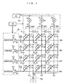
- Reference symbols A1 to A3 denote anodes
- B1 to B4 denote cathodes
- E11 to E34 denote pixels which are located at intersections of the anodes A1 to A3 and the cathodes B1 to B4 and present light emission.
- the respective pixels E11 to E34 are represented by equivalent circuits of a light-emitting element consisting of a diode characteristic and a parasitic capacity connected to this in parallel.
- the parasitic capacity of an arbitrary pixel Exx is assumed to be Cel.
- a drive circuit 10 is connected to the anodes A1 to A3, and a scanning circuit 20 is connected to the cathodes B1 to B4.
- a drive voltage circuit 30 for outputting a drive voltage Va is connected to the drive circuit 10.
- the drive circuit 10 has switches 11 to 13 for selecting the anodes A1 to A3 between the drive circuit 10 and the anodes A1 to A3 and, by turning “ON" these switches 11 to 13, connects DC constant current circuits 14 to 16 serving as drive sources for drive to the anodes A1 to A3.
- the scanning circuit 20 has switches 21 to 24 for sequentially scanning the respective cathodes B1 to B4 as scanning lines, and one ends of the respective switches 21 to 24 are connected to a reverse voltage terminal to which a cutoff voltage Vk volt supplied from a drive voltage circuit 30 is applied and the other ends thereof are connected to a ground terminal of zero volt, and these switches 21 to 24 are changed over to the reverse voltage terminal (unselected) and the ground terminal (selected) in order.
- the drive circuit 10 and the scanning circuit 20 are controlled by a display control circuit 40.
- the switches 11 to 13 of the drive circuit 10 the case in which a current Id is applied to any of the pixels E11 to E34 by the current circuits 14 to 16 is represented as "ON” and the case in which the current Id is no applied is represented as "OFF".
- the switches 21 to 24 of the scanning circuit 20 the case in which the switches 21 to 24 are connected to an anode being scanned among the anodes B1 to B4 is represented as "selected” and the case in which the switches 21 to 24 are connected to an anode not being scanned is represented as "unselected". Consequently, only the pixels, for which the drive circuit 10 is "ON” and the scanning circuit 20 is "selected", among the pixels E11 to E34 emit light.
- capacitors C11 to C34 are connected to each connection point of the pixels E11 to E34 and the anodes A1 to A3, respectively, and the other ends of these capacitors C11 to C34 are collectively connected to a bias circuit 50.
- Vr bias voltage
- an arbitrary capacitor Cxx is selected and connected so as to have an added capacity Cr equal to or more than the parasitic capacity Cel of the pixel Exx to which the one end thereof is connected.
- the parasitic capacity Cel is the same in all the pixels E11 to E34
- only there is one kind of the added capacity Cr only there is one kind of the added capacity Cr.
- the switch 22 of the scanning circuit 20 is changed over to the ground terminal, which is the selected side, and the cathode B2 is scanned.
- the other switches 21, 23, 24 are changed over to the reverse voltage terminal which is the unselected side. Therefore, a potential on the pixel side of the scanning circuit 20 is zero volt for the switch 22 and Vk volt for the other switches.
- a charge Qoff1 to be charged to the other pixel E12, for which the scanning circuit 20 is "selected" , is zero, the charges Qon and Qoff have a relation of Qon > Qoff, and the pixel E12 does not emit light and a current does not flow to the pixel E12.
- a charge Qoff2 to be charged to the pixels E21, E23, E24, E31, E33, E34, for which the drive circuit 10 is "ON” and the scanning circuit 20 is "unselected", is Cel X (Vk - Vf) ⁇ 0. That is, since Vk and Vf have opposite polarities, a difference between them is low compared with Vf, the charges Qon and Qoff2 have a relation of Qon > Qoff2, and the pixel Exx with the charge Qoff2 does not emit light and almost no current flows to the pixel Exx.
- a charge Qoff3 to be charged to the pixels E11, E13, E14, for which the drive circuit 10 is "OFF" and the scanning circuit 20 is "unselected", is Cel X Vk ⁇ 0. That is, since Vk and Vf have opposite polarities, the charges Qon and Qoff3 have a relation of Qon > Qoff3, and the pixel Exx with the charge Qoff3 does not emit light and almost no current flows to the pixel Exx.
- a charge Qc1 to be charged to the capacitors C21 to C24, C31 to C34 connected to the pixel Exx, for which the drive circuit 10 is "ON", is Cr X (Vr - Vf) > 0. This is because Vk and Vf are set to the same polarity.
- a charge Qc2 to be charged to the capacitors C11 to C14 connected to the pixel Exx, for which the drive circuit 10 is "OFF", is Cr X Vr > 0. This is because Vk and Vf are set to the same polarity.
- the switch 23 of the scanning circuit 20 is changed over to the ground terminal, which is the selected side, and the cathode B3 is scanned.
- the other switches 21, 22, 24 are changed over to the reverse voltage terminal which is the unselected side. Therefore, a potential on the pixel side of the scanning circuit 20 is zero volt for the switch 23 and Vk volt for the other switches.
- the drive current Id is flowing to the pixels E13, E33 from the current circuits 14, 16, and a charge Qon to be charged to these pixels E13, E33 is Cel X Vf.
- the charge Qoff of the other pixel Exx is as described above (see Qoff1 to Qoff3), the charges Qon and Qoff have a relation of Qon > Qoff, and the other pixel Exx with the charge Qoff does not emit light.
- the charge charged to the pixel Exx in the above-mentioned example, pixels E11, E13, E14, E31, E33, E34) can be cancelled, and deterioration due to the charge can be improved.
- the charge which is accumulated in the pixel Exx and does not contribute to light emission and the charge accumulated in the capacitor Cxx connected to the pixel Exx are required to have opposite polarities and the latter charge is required to be set larger than the former charge in order to completely eliminate the former charge. Consequently, Cel ⁇ Cr is desirable.
- the present invention can be realized in the same manner as describe above even if a DC constant voltage circuit is used.
- a drive source is a DC drive source
- the bias voltage Vr is a DC voltage in order to charge the added capacity Cr of the capacitor Cxx for canceling a charge to be charged to the parasitic capacity Cel of the pixel Exx.
- JP-A-8-315981 discloses, as shown in Figs. 3 and 4, an OLED which consists of a substrate 100 having anodes A1, A2, A3 ... Ax serving as plural first display electrodes formed on a surface thereof, plural electrical insulating partitions 200 projecting above the substrate 100 which causes at least a part of the anodes A1, A2, A3 ... Ax, at least a single layer of thin film 300 of an organic EL medium formed on the exposed parts of the anodes A1, A2, A3 ... Ax, respectively, and cathodes B1, B2, B3, B4 ... Bx serving as plural second display electrodes formed on this thin film 300.
- a material of the cathodes B1, B2, B3, B4 ... Bx for example, aluminum are evaporated on the partition 200, whereby a conductor film 400 consisting of the same material as the cathodes B1, B2, B3, B4 ... Bx is also formed on the partition 200.
- a dielectric is used as a material forming the partition 200, at least one of the anodes A1, A2, A3 ... Ax (e.g., last Ax) is set as a connection line connected to the bias circuit 50 shown in Figs. 1 and 2 not contributing to display, and the conductor film 400 is electrically connected to this.
- a part of materials thereof enters the through hole 500 to electrically connect the conductor film and the anode Ax, whereby the conductor film 400 is connected to the bias circuit 50 (see Figs. 1 and 2) which is commonly connected and supplies the bias voltage Vr.
- the structure can be simplified.
- the capacitor Cxx can be obtained between the conductor film 400 and the anodes A1, A2, A3 ... Ax-1 on the partition 200.
- the partition 200 is sandwiched by the anodes A1, A2, A3 ... Ax in almost all the portions thereof and, for example, the capacitor Cxx, which is obtained between a conductor film 400a and the anodes A1, A2, A3 ... Ax on a partition 200a located between the cathode B1 and the cathode B2, becomes the capacitor Cxx which affects both a group of the pixels E11, E21, E31 ... formed of the anodes A1, A2, A3 ... and the cathode B1 and a group of the pixels E12, E22, E32 ... formed of the anodes A1, A2, A3 ... and the cathode B2.
- the present invention can be realized not only in the above-mentioned OLED for performing so-called passive matrix display but also in an OLED for performing segment display as long as the present invention can be applied to the OLED in the same manner and the OLED has anodes and cathodes opposed to each other and an organic layer having at least light-emitting layer intervening between both the poles, and presents light emission with the opposed portions as pixels by providing a capacitor having a predetermined added capacity to which a bias voltage in a direction of canceling charges to be charged to a parasitic capacity of the pixels.
Landscapes
- Engineering & Computer Science (AREA)
- Physics & Mathematics (AREA)
- Computer Hardware Design (AREA)
- General Physics & Mathematics (AREA)
- Theoretical Computer Science (AREA)
- Control Of Indicators Other Than Cathode Ray Tubes (AREA)
- Electroluminescent Light Sources (AREA)
- Control Of El Displays (AREA)
Abstract
Description
Claims (6)
- A drive circuit for an organic light-emitting diode which has anodes and cathodes opposed to each other and an organic layer having at least a light-emitting layer intervening between both the poles, and presents light emission with the opposed portions as pixels, characterized in that capacitors having a predetermined added capacity, to which a bias voltage is applied in a direction of canceling charges to be charged to a parasitic capacity of the pixels, are provided.
- A drive circuit for an organic light emitting diode which has plural anodes and plural cathodes intersecting while being opposed to each other and an organic layer having at least a light-emitting layer intervening between both the poles, sets one of both the poles as drive lines and the other of both the poles as scanning lines, and by scanning all of these scanning lines as one field at a predetermined frequency, while sequentially bringing any one of the scanning lines into a selected state, in synchronization with this, connects a drive source to the other of the scanning lines to thereby present light emission with the intersection portions as pixels, characterized in that capacitors having a predetermined added capacity, to which a bias voltage is applied in a direction of canceling charges to be charged to a parasitic capacity of the pixels, are provided.
- A drive circuit for an organic light emitting diode which has plural anodes and plural cathodes intersecting while being opposedto each other and an organic layer having at least a light-emitting layer intervening between both the poles, sets one of both the poles as drive lines and the other of both the poles as scanning lines, has a partition for insulating the scanning lines from each other with a dielectric material on at least one of both the poles, and by scanning all of these scanning lines as one field at a predetermined frequency, while sequentially bringing any one of the scanning lines into a selected state, in synchronization with this, connects a drive source to the other of the scanning lines to thereby present light emission with the intersection portions as pixels, characterized in that capacitors having a predetermined added capacity, to which a bias voltage is applied in a direction of canceling charges to be charged to a parasitic capacity of the pixels between a conductor film formed on the partition and the one of both the poles, are provided.
- A drive circuit for an organic light emitting diode according to claim 3, characterized in that the conductor film is connected to a bias circuit which is commonly connected to supply the bias voltage.
- A drive circuit for an organic light emitting diode according to any one of claims 1 to 3, characterized in that the sum of the added capacity is equal to or more than the parasitic capacity.
- A drive circuit for an organic light emitting diode according to any one of claims 1 to 3, characterized in that the drive source performs a DC current or DC voltage drive, and the bias voltage is a DC voltage.
Applications Claiming Priority (3)
| Application Number | Priority Date | Filing Date | Title |
|---|---|---|---|
| JP2001360597A JP2003162253A (en) | 2001-11-27 | 2001-11-27 | Drive circuit for organic electroluminescent device |
| JP2001360597 | 2001-11-27 | ||
| PCT/JP2002/003704 WO2003046876A1 (en) | 2001-11-27 | 2002-04-12 | Drive circuit for organic el device |
Publications (2)
| Publication Number | Publication Date |
|---|---|
| EP1453029A1 true EP1453029A1 (en) | 2004-09-01 |
| EP1453029A4 EP1453029A4 (en) | 2006-04-26 |
Family
ID=19171380
Family Applications (1)
| Application Number | Title | Priority Date | Filing Date |
|---|---|---|---|
| EP02718572A Withdrawn EP1453029A4 (en) | 2001-11-27 | 2002-04-12 | DRIVE CIRCUIT FOR ORGANIC ELECTROLUMINESCENT DIODE DEVICE |
Country Status (4)
| Country | Link |
|---|---|
| US (1) | US6803729B2 (en) |
| EP (1) | EP1453029A4 (en) |
| JP (1) | JP2003162253A (en) |
| WO (2) | WO2003046876A1 (en) |
Families Citing this family (8)
| Publication number | Priority date | Publication date | Assignee | Title |
|---|---|---|---|---|
| JP3737889B2 (en) * | 1998-08-21 | 2006-01-25 | パイオニア株式会社 | Light emitting display device and driving method |
| TWI229313B (en) * | 2003-09-12 | 2005-03-11 | Au Optronics Corp | Display pixel circuit and driving method thereof |
| JP2005148248A (en) * | 2003-11-13 | 2005-06-09 | Tohoku Pioneer Corp | Spontaneous light emitting display device |
| US7358939B2 (en) * | 2004-07-28 | 2008-04-15 | Leadis Technology, Inc. | Removing crosstalk in an organic light-emitting diode display by adjusting display scan periods |
| JP2006227337A (en) * | 2005-02-18 | 2006-08-31 | Fuji Electric Holdings Co Ltd | Organic EL display device and driving method thereof |
| EP1873745A1 (en) | 2006-06-30 | 2008-01-02 | Deutsche Thomson-Brandt Gmbh | Method and apparatus for driving a display device with variable reference driving signals |
| JP5394106B2 (en) * | 2009-03-26 | 2014-01-22 | パナソニック株式会社 | Power supply method for planar light emitting device |
| KR20120062252A (en) * | 2010-12-06 | 2012-06-14 | 삼성모바일디스플레이주식회사 | Pixel and organic light emitting display device using the pixel |
Family Cites Families (14)
| Publication number | Priority date | Publication date | Assignee | Title |
|---|---|---|---|---|
| JPH03102411A (en) | 1989-09-18 | 1991-04-26 | Fujitsu Ltd | Operating circuit for composite power supply |
| JP2663648B2 (en) * | 1989-09-25 | 1997-10-15 | ミノルタ株式会社 | Organic electroluminescence device |
| JPH03110788A (en) | 1989-09-25 | 1991-05-10 | Hitachi Chem Co Ltd | Manufacture of membranous el element |
| JP3169974B2 (en) | 1991-04-08 | 2001-05-28 | パイオニア株式会社 | Organic electroluminescent display device and driving method thereof |
| JP3813217B2 (en) | 1995-03-13 | 2006-08-23 | パイオニア株式会社 | Method for manufacturing organic electroluminescence display panel |
| JPH0832307A (en) | 1994-07-20 | 1996-02-02 | Oki Electric Ind Co Ltd | Dielectric device |
| JP3507239B2 (en) | 1996-02-26 | 2004-03-15 | パイオニア株式会社 | Method and apparatus for driving light emitting element |
| US6157356A (en) * | 1996-04-12 | 2000-12-05 | International Business Machines Company | Digitally driven gray scale operation of active matrix OLED displays |
| JP3767877B2 (en) * | 1997-09-29 | 2006-04-19 | 三菱化学株式会社 | Active matrix light emitting diode pixel structure and method thereof |
| JP2001056668A (en) * | 1999-08-20 | 2001-02-27 | Nippon Seiki Co Ltd | Driving circuit of organic electroluminescence device |
| KR100681924B1 (en) * | 2000-02-24 | 2007-02-15 | 코닌클리케 필립스 일렉트로닉스 엔.브이. | Organic LED display with improved charging of pixel capacity |
| JP2002108284A (en) * | 2000-09-28 | 2002-04-10 | Nec Corp | Organic el display device and its drive method |
| JP3494146B2 (en) * | 2000-12-28 | 2004-02-03 | 日本電気株式会社 | Organic EL drive circuit, passive matrix organic EL display device, and organic EL drive method |
| JP2002343561A (en) * | 2001-05-22 | 2002-11-29 | Nippon Seiki Co Ltd | Drive circuit of organic electroluminescence element |
-
2001
- 2001-11-27 JP JP2001360597A patent/JP2003162253A/en active Pending
-
2002
- 2002-04-12 WO PCT/JP2002/003704 patent/WO2003046876A1/en not_active Ceased
- 2002-04-12 US US10/250,931 patent/US6803729B2/en not_active Expired - Lifetime
- 2002-04-12 EP EP02718572A patent/EP1453029A4/en not_active Withdrawn
- 2002-11-15 WO PCT/JP2002/011982 patent/WO2003046875A1/en not_active Ceased
Also Published As
| Publication number | Publication date |
|---|---|
| WO2003046876A1 (en) | 2003-06-05 |
| US20040047143A1 (en) | 2004-03-11 |
| WO2003046875A1 (en) | 2003-06-05 |
| JP2003162253A (en) | 2003-06-06 |
| US6803729B2 (en) | 2004-10-12 |
| EP1453029A4 (en) | 2006-04-26 |
Similar Documents
| Publication | Publication Date | Title |
|---|---|---|
| CN100410990C (en) | Organic EL display device and organic EL display device driving method | |
| JP3613451B2 (en) | Driving device and driving method for multicolor light emitting display panel | |
| US7061452B2 (en) | Spontaneous light-emitting display device | |
| JP3568097B2 (en) | Light emitting display and driving method thereof | |
| KR101282399B1 (en) | Display device and driving method thereof | |
| US6714177B1 (en) | Light-emitting display device and driving method therefor | |
| JP2002108284A (en) | Organic el display device and its drive method | |
| US6552703B1 (en) | Display apparatus of capacitive light emitting devices | |
| US6803729B2 (en) | Drive circuit for organic EL device | |
| US20040189560A1 (en) | Drive device for light-emitting display panel | |
| JP3552150B2 (en) | Color display | |
| JP2000105564A (en) | Capacitive light emitting display device and driving method thereof | |
| EP1457961A2 (en) | Display device and display panel driving method | |
| JP3646916B2 (en) | Multicolor light emitting display panel drive device | |
| JP2001042825A (en) | Driving device of multicolor light emitting display panel | |
| JP2002328650A (en) | Drive circuit for organic electric field light emitting element | |
| JP2002343561A (en) | Drive circuit of organic electroluminescence element | |
| CN1822080B (en) | Organic EL display device and method for driving same | |
| JP2000148086A (en) | Light emitting display device and driving method therefor | |
| KR100753866B1 (en) | OLED display device using Zener diode | |
| JP2001109429A (en) | Device for driving light emitting display panel | |
| JP2005070619A (en) | Organic EL panel drive circuit and organic EL panel drive method | |
| KR100469975B1 (en) | Apparatus for driving metal-insulator-metal field emission display using constant-current circuit | |
| JP2001056668A (en) | Driving circuit of organic electroluminescence device | |
| KR100498283B1 (en) | Structure for matrix of mim fed |
Legal Events
| Date | Code | Title | Description |
|---|---|---|---|
| PUAI | Public reference made under article 153(3) epc to a published international application that has entered the european phase |
Free format text: ORIGINAL CODE: 0009012 |
|
| 17P | Request for examination filed |
Effective date: 20030815 |
|
| AK | Designated contracting states |
Kind code of ref document: A1 Designated state(s): AT BE CH CY DE DK ES FI FR GB GR IE IT LI LU MC NL PT SE TR |
|
| AX | Request for extension of the european patent |
Extension state: AL LT LV MK RO SI |
|
| A4 | Supplementary search report drawn up and despatched |
Effective date: 20060309 |
|
| RIC1 | Information provided on ipc code assigned before grant |
Ipc: G09G 3/32 20060101ALI20060303BHEP Ipc: H05B 33/08 20060101ALI20060303BHEP Ipc: G09G 3/30 20060101AFI20030612BHEP |
|
| 17Q | First examination report despatched |
Effective date: 20060814 |
|
| GRAP | Despatch of communication of intention to grant a patent |
Free format text: ORIGINAL CODE: EPIDOSNIGR1 |
|
| RBV | Designated contracting states (corrected) |
Designated state(s): DE FR GB IT |
|
| STAA | Information on the status of an ep patent application or granted ep patent |
Free format text: STATUS: THE APPLICATION IS DEEMED TO BE WITHDRAWN |
|
| 18D | Application deemed to be withdrawn |
Effective date: 20080701 |