EP1452904A2 - Light deflector and optical switch including same - Google Patents
Light deflector and optical switch including same Download PDFInfo
- Publication number
- EP1452904A2 EP1452904A2 EP04250393A EP04250393A EP1452904A2 EP 1452904 A2 EP1452904 A2 EP 1452904A2 EP 04250393 A EP04250393 A EP 04250393A EP 04250393 A EP04250393 A EP 04250393A EP 1452904 A2 EP1452904 A2 EP 1452904A2
- Authority
- EP
- European Patent Office
- Prior art keywords
- light
- photonic crystal
- electro
- dielectric
- optic
- Prior art date
- Legal status (The legal status is an assumption and is not a legal conclusion. Google has not performed a legal analysis and makes no representation as to the accuracy of the status listed.)
- Withdrawn
Links
Images

Classifications
-
- G—PHYSICS
- G02—OPTICS
- G02F—OPTICAL DEVICES OR ARRANGEMENTS FOR THE CONTROL OF LIGHT BY MODIFICATION OF THE OPTICAL PROPERTIES OF THE MEDIA OF THE ELEMENTS INVOLVED THEREIN; NON-LINEAR OPTICS; FREQUENCY-CHANGING OF LIGHT; OPTICAL LOGIC ELEMENTS; OPTICAL ANALOGUE/DIGITAL CONVERTERS
- G02F1/00—Devices or arrangements for the control of the intensity, colour, phase, polarisation or direction of light arriving from an independent light source, e.g. switching, gating or modulating; Non-linear optics
- G02F1/01—Devices or arrangements for the control of the intensity, colour, phase, polarisation or direction of light arriving from an independent light source, e.g. switching, gating or modulating; Non-linear optics for the control of the intensity, phase, polarisation or colour
- G02F1/03—Devices or arrangements for the control of the intensity, colour, phase, polarisation or direction of light arriving from an independent light source, e.g. switching, gating or modulating; Non-linear optics for the control of the intensity, phase, polarisation or colour based on ceramics or electro-optical crystals, e.g. exhibiting Pockels effect or Kerr effect
- G02F1/035—Devices or arrangements for the control of the intensity, colour, phase, polarisation or direction of light arriving from an independent light source, e.g. switching, gating or modulating; Non-linear optics for the control of the intensity, phase, polarisation or colour based on ceramics or electro-optical crystals, e.g. exhibiting Pockels effect or Kerr effect in an optical waveguide structure
-
- G—PHYSICS
- G02—OPTICS
- G02F—OPTICAL DEVICES OR ARRANGEMENTS FOR THE CONTROL OF LIGHT BY MODIFICATION OF THE OPTICAL PROPERTIES OF THE MEDIA OF THE ELEMENTS INVOLVED THEREIN; NON-LINEAR OPTICS; FREQUENCY-CHANGING OF LIGHT; OPTICAL LOGIC ELEMENTS; OPTICAL ANALOGUE/DIGITAL CONVERTERS
- G02F1/00—Devices or arrangements for the control of the intensity, colour, phase, polarisation or direction of light arriving from an independent light source, e.g. switching, gating or modulating; Non-linear optics
- G02F1/29—Devices or arrangements for the control of the intensity, colour, phase, polarisation or direction of light arriving from an independent light source, e.g. switching, gating or modulating; Non-linear optics for the control of the position or the direction of light beams, i.e. deflection
- G02F1/31—Digital deflection, i.e. optical switching
- G02F1/313—Digital deflection, i.e. optical switching in an optical waveguide structure
-
- G—PHYSICS
- G02—OPTICS
- G02F—OPTICAL DEVICES OR ARRANGEMENTS FOR THE CONTROL OF LIGHT BY MODIFICATION OF THE OPTICAL PROPERTIES OF THE MEDIA OF THE ELEMENTS INVOLVED THEREIN; NON-LINEAR OPTICS; FREQUENCY-CHANGING OF LIGHT; OPTICAL LOGIC ELEMENTS; OPTICAL ANALOGUE/DIGITAL CONVERTERS
- G02F2202/00—Materials and properties
- G02F2202/32—Photonic crystals
Definitions
- the present invention relates to light deflectors composed of electro-optic photonic crystals and optical switches including the same.
- photonic crystals Materials having periodic refractive index structures at a scale on the order of the wavelength of light are known as photonic crystals.
- photonic crystals a bandgap that forbids the existence of light with wavelengths corresponding to the period, i.e., a so-called "photonic bandgap", appears, and thereby the existence and propagation of light in a predetermined wavelength band are forbidden. Accordingly, photonic crystals are considered to have the potential to freely control light, and they are thus receiving attention as next-generation electronic and optoelectronic materials.
- the present inventor has been carrying out research on such photonic crystals and has found a novel photonic crystal by treating photonic crystals with two-dimensional or three-dimensional periodic structures using a technique invented by the present inventor, and as a result, the present invention on a light deflector and an optical switch has been achieved.
- an optical modulator using the electro-optical effect in LiNbO 3 or the like is generally known, for example, as disclosed in Japanese Unexamined Patent Application Publication No. 2002-196296.
- a light deflector is composed of an electro-optic photonic crystal in which the refraction angle of light incident from outside can be controlled by controlling an electric field applied to the electro-optic photonic crystal so as to change the refractive index of the material constituting the photonic crystal and in which the change in the refraction angle in response to the change in the unit refractive index of the material is 10 3 degrees or more, and preferably 10 4 degrees or more.
- the light deflector of the present invention uses the superprism effect in which the refraction angle is sensitively changed by strong anisotropy in the dispersion surface of the electro-optic photonic crystal.
- the refractive index of the material constituting the photonic crystal can be changed, and thereby the refraction angle of light incident from outside can be changed. Consequently, by controlling the electric field applied to the electro-optic photonic crystal, the refraction angle of light entering the electro-optic photonic crystal from outside can be controlled and the direction of light emitted from the electro-optic photonic crystal can be controlled.
- the refraction angle of light entering the electro-optic photonic crystal from outside can be changed rapidly in response to the change in the electric field applied to the electro-optic photonic crystal.
- the electro-optic photonic crystal can be miniaturized, a miniature light deflector can be produced.
- the electro-optic photonic crystal includes a combination of a plurality of first dielectric members and a second dielectric member or a combination of a first dielectric member and a plurality of second dielectric members, the first dielectric member being composed of a material with a dielectric constant changeable by an electric field (a first material with dielectric constant changeable by electric field) in which the dielectric constant is controlled by an electric field, the second dielectric member having a different dielectric constant from that of the first dielectric member, wherein a plurality of first dielectric members or second dielectric members are periodically arrayed separately from each other, thus forming a periodic structure (first periodic structure); the other dielectric member is disposed in the space of the periodic arrangement; and the first dielectric member is composed of a material selected from the group consisting of LiNbO 3 , LiTaO 3 , BaTiO 3 , GaAs, ZnO, NH 4 H 2 PO 4 , and KH 2 PO 4 .
- the refractive index of the first dielectric member is changed, and consequently, the refraction angle of light incident from outside is changed.
- the first dielectric member is composed of a material which shows electro-optical characteristics in which the magnitude of the refractive index changes as the magnitude of the electric field applied is changed.
- the material for the second dielectric member air or the like is used.
- a plurality of regions in which air is present as the second dielectric members may be periodically arrayed separately from each other in the first dielectric member.
- a plurality of first dielectric members may be periodically arrayed separately from each other and a region in which air is present as the second dielectric member may be disposed in the space of the periodic arrangement.
- the direction of the electric field applied to the electro-optic photonic crystal preferably corresponds to the direction with a higher electro-optic coefficient of the electro-optic photonic crystal, and more preferably corresponds to the direction with a higher electro-optic coefficient of the crystal constituting the first dielectric member.
- the electric field is preferably applied in the c-axis direction. In view of the shape, the electric field is preferably applied in the direction with a smaller thickness of the electro-optic photonic crystal.
- the direction of the light incident from outside corresponds to a direction other than the direction of the normal line of the dispersion surface of the electro-optic photonic crystal, or a direction other than the direction perpendicular to the dispersion surface of the electro-optic photonic crystal.
- the direction of the light incident from outside corresponds to the direction of the normal line of the dispersion surface of the electro-optic photonic crystal, the light entering the electro-optic photonic crystal is transmitted without being refracted, resulting in no change to the refraction angle.
- the light deflector of the present invention may be provided with electrodes for applying an electric field to the electro-optic photonic crystal.
- the light deflector of the present invention may be provided with a variable power unit which is capable of applying a DC or AC electric field to the electro-optic photonic crystal and in which the magnitude of the voltage (electric field) applied can be varied.
- the light deflector of the present invention may be provided with a unit for introducing light into the electro-optic photonic crystal.
- an optical switch in another aspect of the present invention, includes the light deflector of the present invention and a photonic crystal waveguide, the photonic crystal waveguide having a photonic bandgap for light of a predetermined wavelength and also having at least one waveguide which passes the light of the predetermined wavelength.
- the optical switch of the present invention as the light entering the electro-optic photonic crystal constituting the light deflector, light in a wavelength band whose existence is forbidden by the photonic bandgap is used.
- the optical switch having such a structure, when the magnitude of the electric field applied to the electro-optic photonic crystal constituting the light deflector is changed, the refraction angle of light of a predetermined wavelength entering the electro-optic photonic crystal is changed, and the direction of light of the predetermined wavelength emitted from the electro-optic photonic crystal (outgoing light) is changed. Consequently, the outgoing light is transmitted through a waveguide which is present in the direction of the emitted light of the predetermined wavelength, among the waveguides provided in the photonic crystal waveguide. Therefore, the direction in which the transmitted light of the predetermined wavelength passes through can be switched at high speed. Since the photonic crystal waveguide can also be miniaturized along with the electro-optic photonic crystal, it is possible to produce a miniature optical switch.
- the photonic crystal waveguide provided in the optical switch of the present invention includes a third dielectric member composed of a second material with a dielectric constant changeable by an electric field in which the dielectric constant is controlled by an electric field and a fourth dielectric member having a different dielectric constant from that of the third dielectric member, wherein a plurality of third dielectric members or fourth dielectric members are periodically arrayed separately from each other to form a periodic structure (second periodic structure); and the other dielectric member is disposed in the space of the periodic arrangement.
- the photonic crystal waveguide also includes a region in which the periodic structure is omitted at least in part, the region being a waveguide, and a plurality of waveguides may be provided in response to the refraction angles of light entering the light deflector.
- the periodic structure has a photonic bandgap for light of a predetermined wavelength.
- the photonic crystal by partially omitting the periodic structure in which a plurality of third dielectric members or fourth dielectric members are periodically arrayed separately from each other, it is possible to introduce a defect corresponding to the portion omitted. A localized state appears in the photonic bandgap due to the defect, and light is trapped therein. By continuously connecting defects, it is possible to guide light along the defects, and a waveguide can be formed along the portions in which the periodic structure is omitted. Consequently, it is possible to provide a photonic crystal waveguide in which light can be guided along the waveguide.
- the outgoing light is transmitted through the waveguide corresponding to the refraction angle of light of the predetermined wavelength, among the waveguides provided in the photonic crystal waveguide. Therefore, the direction of emission of the transmitted light of the predetermined wavelength can be switched at high speed.
- the third dielectric member used in the photonic crystal waveguide may be composed of a material selected from the group consisting of Si, GaP, GaAs, InP, ZnTe, Ge, LiNbO 3 , LiTaO 3 , BaTiO 3 , ZnO, NH 4 H 2 PO 4' and KH 2 PO 4 .
- the third dielectric member By forming the third dielectric member using such a material, it is possible to utilize a high dielectric constant and a high refractive index.
- the fourth dielectric member used in the photonic crystal waveguide may be composed of a material selected from the group consisting of air and liquid crystal.
- the array period of the periodic structure of the dielectric members preferably corresponds to a fraction of the wavelength of predetermined light, and by properly designing the period, the lattice shape of the array, the refractive indexes of the dielectric members, the shape, etc., it is possible to control the photonic bandgap.
- FIG. 1 is a plan view which schematically shows a structure of an optical switch in an embodiment of the present invention
- FIG. 2 is a sectional view of the optical switch shown in FIG. 1.
- the optical switch in this embodiment includes a light deflector A and a photonic crystal waveguide B.
- the light deflector A uses the superprism effect in which the refraction angle of incident light is sensitively changed by strong anisotropy in the wave-vector surface (dispersion surface) of an electro-optic photonic crystal.
- the light deflector A is composed of an electro-optic photonic crystal which includes conductive substrates 1 and 2 which are placed substantially parallel to each other with a distance therebetween; a transparent sealing member 5 interposed between the peripheries of the substrates 1 and 2 and surrounding the void between the substrates 1 and 2; a plurality of cylinders (first dielectric members) 3 which are interposed between the substrates 1 and 2 and stand at an interval corresponding to a fraction of the wavelength of light; and air (a second dielectric member) 6 filled in the space surrounded by the substrates 1 and 2 and the sealing member 5 and around the cylinders 3. That is, in the electro-optic photonic crystal, a plurality of cylinders 3 are periodically arrayed separately from each other, and the region in which the air 6 is present is disposed in the space of the periodic arrangement.
- a light source 4 such as a laser emission device, which is capable of emitting light of a desired wavelength is placed in the exterior of the transparent sealing member 5, separately from the electro-optic photonic crystal.
- Light L of a predetermined wavelength e.g., 1,550 nm or 1,310 nm
- a predetermined wavelength is emitted from the light source 4 so as to be incident on the void between the substrates 1 and 2 constituting the electro-optic photonic crystal through the transparent sealing member 5.
- the incident light L entering the electro-optic photonic crystal from outside light in a wavelength band whose existence is forbidden by the photonic bandgap of the photonic crystal waveguide B is used.
- the photonic bandgap is about 100 nm (1.45 ⁇ m to 1.55 ⁇ m).
- the substrates 1 and 2 are composed of a high-dielectric material (first high-dielectric material), such as ion-doped, highly conductive LiNbO 3 , and oxide layers 7 and 8 are disposed on the opposing surfaces of the substrates 1 and 2, the oxide layers 7 and 8 being formed by surface oxidation or the like of the LiNbO 3 substrates.
- first high-dielectric material such as ion-doped, highly conductive LiNbO 3
- oxide layers 7 and 8 are disposed on the opposing surfaces of the substrates 1 and 2, the oxide layers 7 and 8 being formed by surface oxidation or the like of the LiNbO 3 substrates.
- Each material has a high dielectric constant and shows electro-optic characteristics in which the refractive index changes as the magnitude of an electric field applied is changed.
- the refraction angle of light incident from outside must be sensitively changed when the magnitude of an applied electric field is changed.
- the electro-optic photonic crystal does not necessarily have a bandgap.
- the difference in refractive index between the cylinder (first dielectric member) 3 and the second dielectric member 6 may be small.
- the second dielectric member 6 must have a different dielectric constant from that of the first dielectric member 3. Consequently, the second dielectric member 6 may be composed of a liquid crystal instead of air.
- the refractive index of air is 1 both in the normal state (in the absence of an applied electric field) and in the presence of an applied electric field. With respect to a liquid crystal, the difference in dielectric constant between in the presence of an applied electric field and in the absence of an applied electric field is more noticeable compared with air.
- the cylinders 3 which are the first dielectric members are formed by etching or the like of one of the substrates 1 and 2.
- a plurality of cylinders 3 are formed at an interval corresponding to a fraction of the wavelength of predetermined light L emitted from the light source 4, and a set of the plurality of cylinders 3 constitutes a periodic structure (first periodic structure) 3A.
- the distance P 1 between the centers of two adjacent cylinders 3 is set at about a fraction of the wavelength ⁇ of the predetermined light L (0.2 ⁇ to 0.8 ⁇ ), and the diameter D 1 of the cylinder 3 is set at about a fraction of the wavelength ⁇ of the predetermined light L (0.2 ⁇ to 0.8 ⁇ ). More specifically, when light with a wavelength of 1,550 nm is used, for example, the distance P 1 between the centers of two adjacent cylinders 3 may be selected from the range of 0.3 to 1.1 ⁇ m, and the diameter D 1 of the cylinder 3 may be selected from the range of 0.14 to 0.5 ⁇ m.
- GaAs used as a material for the first high-dielectric material constituting the first dielectric members 3 since GaAs is used as a semiconductor material and can be imparted with conductivity by ion doping or the like, it is also possible to use GaAs as electrodes for applying an electric field to the electro-optic photonic crystal.
- GaAs When LiNbO 3 or the like is used as the first high-dielectric material constituting the first dielectric members 3, electrodes are provided on the respective outer surfaces of the substrates 1 and 2, and the electrodes are used for applying an electric field to the electro-optic photonic crystal.
- a variable power unit 10 is connected to the substrates 1 and 2 by interconnect lines 9A and 9B, respectively.
- a switch 10a which is built in the interconnect line 9B, an alternating current (electric field) can be applied to the plurality of cylinders 3 interposed between the substrates 1 and 2.
- the switch 10a By turning off the switch 10a, the application of the alternating current (electric field) can be stopped.
- the variable power unit 10 is also constructed so that the magnitude of the voltage (electric field) applied to the substrates 11 and 12 can be changed.
- Equation (1) relates to the characteristics of the light deflector A in this embodiment.
- n is the refractive index of the electro-optic material (the refractive index of the first dielectric member 3 in this embodiment)
- ⁇ r is the refraction angle of light entering the electro-optic photonic crystal from outside
- ⁇ 33 is the electro-optic coefficient (Pockels coefficient)
- E is the intensity of an electric field applied to the electro-optic material (the first dielectric member 3 in this embodiment)
- (1/2) ⁇ ⁇ 33 n 3 E represents a difference in refractive index due to the electro-optic effect.
- the light deflector A is composed of the electro-optic photonic crystal
- the refractive index of the plurality of cylinders (first dielectric members) 3 changes, resulting in a change in the refractive index of the entire electro-optic photonic crystal. Consequently, the refraction angle of light L entering the electro-optic photonic crystal from outside can be changed.
- the change in the refraction angle is 10 3 degrees or more and preferably 10 4 degrees or more, i.e., ⁇ r/ ⁇ n is 10 3 degrees or more and preferably 10 4 degrees or more.
- ⁇ r/ ⁇ n is less than 10 3 degrees, the size of the device becomes about 1 cm or more, which is undesirable.
- the direction of the electric field applied to the electro-optic photonic crystal preferably corresponds to the direction with a higher electro-optic coefficient of the electro-optic photonic crystal, and more preferably corresponds to the direction with a higher electro-optic coefficient of the crystal constituting the first dielectric member 3.
- the electric field is preferably applied in the c-axis direction of the crystal.
- the electric field is preferably applied in the direction with a smaller thickness of the electro-optic photonic crystal.
- the direction of the incident light L entering the electro-optic photonic crystal from outside corresponds to a direction other than the direction of the normal line of the dispersion surface (wave-vector surface) of the electro-optic photonic crystal, or a direction other than the direction perpendicular to the dispersion surface of the electro-optic photonic crystal.
- the incident direction of light L is inclined at several angles with respect to the direction of the normal line of the dispersion surface (wave-vector surface).
- the incident direction of light entering the electro-optic photonic crystal corresponds to the direction of the normal line of the dispersion surface of the electro-optic crystal, the light entering the electro-optic photonic crystal is transmitted without being refracted, resulting in no change to the refraction angle.
- the refractive index of the first dielectric member 3 is the same as that in the normal state.
- the light L is refracted at a normal refraction angle, and light L 1 refracted at the normal refraction angle is emitted toward the photonic crystal waveguide B.
- the first dielectric member 3 When an electric field is applied to the light deflector A, the first dielectric member 3 has a refractive index that is different from the normal refractive index. As shown in FIG. 1, when light L of a predetermined wavelength from the light source 4 is incident on the electro-optic photonic crystal in the presence of an applied electric field, the light L is refracted at a refraction angle that is different from the normal refraction angle, and light L 2 refracted at the refraction angle that is different from the normal refraction angle is emitted toward the photonic crystal waveguide B.
- the difference in refraction angle between the light L 1 and the light L 2 corresponds to ⁇ r and the difference in the refractive index of the first dielectric member (electro-optic member) 3 between in the presence of an applied electric field and in the absence of an applied electric field corresponds to ⁇ n.
- the distance P between the position of the electro-optic photonic crystal from which light is emitted in the presence of an applied electric field and the position of the electro-optic photonic crystal from which light is emitted in the absence of an applied electric field is sufficiently large, and moreover, the direction of light emitted from the electro-optic photonic crystal can be changed.
- the refraction angle of light entering the electro-optic photonic crystal from outside can be controlled, and the direction of light emitted from the electro-optic photonic crystal can be controlled.
- the refraction angle of light entering the electro-optic photonic crystal from outside can be rapidly changed in response to the change in the electric field applied to the electro-optic photonic crystal. Since the electro-optic photonic crystal can be miniaturized, a miniature light deflector can be produced.
- the photonic crystal waveguide B has a photonic bandgap for light L of a predetermined wavelength.
- a plurality of third dielectric members 13 are periodically arrayed separately from each other to form a periodic structure (second periodic structure) 13A, and the region in which the air 16 is present is disposed in the space of the periodic arrangement.
- the second periodic structure 13A is partially omitted, and regions in which the second periodic structure 13A is omitted correspond to the waveguides 22.
- the substrates 11 and 12 are composed of a high-dielectric material (second high-dielectric material), such as Si, and oxide layers 17 and 18 are disposed on the opposing surfaces of the substrates 11 and 12, the oxide layers 17 and 18 being formed by surface oxidation or the like of the Si substrates.
- Each material has a high dielectric constant.
- the difference between the refractive index of the cylinders (third dielectric members) 13 which are composed of a second material with a dielectric constant changeable by an electric field in which the dielectric constant is controlled by an electric field and the refractive index of the fourth dielectric member 16 is preferably large because the bandgap can be increased. Therefore, the fourth dielectric member 16 is preferably composed of a material with a refractive index of about 3 or more.
- the cylinders 13 which are the third dielectric members are formed by etching or the like of one of the substrates 11 and 12.
- a plurality of cylinders 13 are formed at an interval corresponding to a fraction of the wavelength of predetermined light emitted from the light source 4, and a group of the plurality of cylinders 13 constitutes the periodic structure (second periodic structure) 13A.
- the distance P 2 between the centers of two adjacent cylinders 13 is set at about a fraction of the wavelength ⁇ of the predetermined light (0.2 ⁇ to 0.8 ⁇ ), and the diameter D 2 of the cylinder 13 is set at about a fraction of the wavelength X of the predetermined light (0.2 ⁇ to 0.8 ⁇ ).
- the distance P 2 between the centers of two adjacent cylinders 13 may be selected from the range of 0.3 to 1.1 ⁇ m, and the diameter D 2 of the cylinder 13 may be selected from the range of 0.14 to 0.5 ⁇ m.
- the fourth dielectric member 16 may be composed of a liquid crystal instead of air.
- a liquid crystal for example, a nematic liquid crystal with a dielectric constant of 2 to 3 may be used.
- regions in which parts of the cylinders 13 are linearly omitted are provided in the second periodic structure 13A.
- a plurality of regions in which the cylinders 13 are partially omitted extending from the light deflector A side to the opposite side are provided to form a plurality of waveguides 22 (two waveguides in this embodiment).
- the plurality of waveguides 22 are formed corresponding to the refraction angles of light L of a predetermined wavelength entering the light deflector A from outside, i.e., corresponding to the directions of light of a predetermined wavelength emitted from the light deflector A.
- a waveguide 22a is provided corresponding to the refraction angle of light L with a predetermined wavelength entering the light deflector A in the absence of an applied electric field (corresponding to light L 1 of the predetermined wavelength emitted from the light deflector A in the absence of an applied electric field).
- a waveguide 22b is provided corresponding to the refraction angle of light L of a predetermined wavelength entering the light deflector A from outside (corresponding to light L 2 of the predetermined wavelength emitted from the light deflector A in the presence of an applied electric field).
- a photonic bandgap for light is generated because the periodic structure 13A formed by the plurality of cylinders 13 and air 16 filled in the space between the cylinders 13 constitute a photonic crystal.
- the photonic bandgap corresponds to a frequency band in which light of predetermined frequencies is not transmitted.
- the photonic bandgap is 1,450 to 1,550 nm (0.86 to 0.8 eV). Consequently, the region in which the periodic structure 13A including the periodic arrangement of the cylinders 13 reflects and does not transmit light with wavelengths in the range of 1,450 to 1,550 nm.
- the light L When light L of a predetermined wavelength from the light source 4 is incident on the light deflector A in the presence of an applied electric field, the light L is refracted at a refraction angle which is different from the normal refraction angle by ⁇ r, and light L 2 refracted at the refraction angle which is different from the normal refraction angle is emitted toward the photonic crystal waveguide B.
- the light L 2 passes through the waveguide 22b and emitted from the emission side of the photonic crystal waveguide B (opposite to the light deflector A side) at a position different from the position at which the light L 1 is emitted.
- a surface of the substrate 11 composed of Si is subjected to oxidation treatment to form the oxide layer 17.
- the transparent sealing member is placed along the periphery of the oxide layer 17 on the substrate 11.
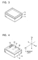
- a surface of the other substrate 12 composed of Si is etched by chemical etching or physical etching, such as ion beam etching, and many cylinders (third dielectric members) 13 are thereby formed on the substrate 12 as shown in FIG. 4.
- the waveguides 22 are formed.
- a resist is applied onto the surface of the substrate 12, and drawing is performed by an exposure apparatus or the like so as to correspond to the periodic structure of the cylinders.
- the resist in the drawn regions only are removed by dissolution with a developer to form many holes.
- Immersion into an etchant is performed using the holes.
- the Si substrate is etched by SF 6 plasma or the like to form a plurality of cylinders 13.
- a resist composed of poly(methyl methacrylate) (PMMA) or the like which is sensitive to electron beam exposure is applied onto a Si wafer, and a periodic structure is drawn thereon by an electron beam.
- the PMMA resist in the drawn regions are removed by dissolution with a developer to form windows.
- Iron atoms with a thickness of about 1 nm are vapor-deposited, and then the PMMA resist is removed by a lift-off method. Thereby, iron atoms aggregate on the surface of the substrate, and iron clusters can be formed only on the regions in which windows are opened corresponding to the regions drawn by the electron beam.
- iron clusters and their peripheries only remain without being etched.
- Many Si cylinders with a uniform size can be fabricated.
- the iron clusters themselves do not function as etching masks, but function as nuclei for forming etching masks with a uniform size by condensing the reaction products, such as S x F x , from the plasma.
- iron clusters are capable of forming masks with high etching resistance, and by using such a function, it is possible to fabricate Si cylinders with a uniform size.
- the light deflector A provided on the optical switch shown in FIG. 1 can be fabricated as in the photonic crystal waveguide B described above except that defects are not introduced into the periodic structure and that the first high-dielectric material is used for the two substrates.
- the optical switch of this embodiment if a plurality of waveguides 22 corresponding to the refraction angles of light L with a predetermined wavelength entering the light deflector A are provided in the photonic crystal waveguide B in advance, when the refraction angle of the light L of the predetermined wavelength entering the electro-optic photonic crystal is changed in response to a change in the magnitude of an electric field applied to the electro-optic photonic crystal and the direction of light of the predetermined wavelength emitted from the electro-optic photonic crystal (outgoing light) is changed, the outgoing light is transmitted (passes) through the waveguide 22 corresponding to the refraction angle of the light of the predetermined wavelength, among a plurality of waveguides 22 provided in the photonic crystal waveguide B.
- the direction emission of the transmitted light of the predetermined wavelength can be switched at high speed.
- the switching rate can be set at ⁇ sec or more. Since the photonic crystal waveguide B can also be miniaturized along with the electro-optic photonic crystal constituting the light deflector A, a miniature optical switch can be produced, for example, at a size of several millimeters.
- the portion of the sealing member 5 or sealing member 15 on which light is incident must be translucent or transparent, and the portion from which light is emitted must be translucent or transparent. Therefore, preferably, the entire sealing member 5 or sealing member 15 is transparent.
- the electro-optic photonic crystal having the structure shown in FIG. 1 only a plurality of cylinders 3 must be composed of the first high-dielectric material, and it is not necessary to form the entire substrates 1 and 2 using the first high-dielectric material.
- the substrates 1 and 2 may be composed of other commonly used material and the cylinders 3 only may be composed of the first high dielectric material.
- the substrates 11 and 12 may be composed of a commonly used material other than the second high-dielectric material and the cylinders 13 only may be composed of the second high-dielectric material.
- metal electrodes or electrode layers such as transparent electrode layers may be separately formed on the air 6 sides of the substrates 1 and 2 so that an electric field can be applied to the periodic structure 3A from the electrode layers.
- a conductor such as ion-doped LiNbO 3 .
- the substrates 1 and 2 are composed of an insulator which is not a high-dielectric material; electrode layers, such as indium tin oxide (ITO) layers or metal electrode layers, are separately formed on the opposing surfaces of the insulating substrates; and a plurality of cylinders 3 composed of the first high-dielectric material are interposed between the insulating substrates.
- ITO indium tin oxide
- the periodic structures provided on the electro-optic photonic crystal and the photonic crystal waveguide are composed of sets of cylinders composed of high-dielectric materials, two-dimensional periodic structures are formed.
- the periodic structures may be three-dimensional.
- a three-dimensional structure in which cylinders are assembled into a lattice-shape may be acceptable.
- the three-dimensional structure may be assembled into various shapes, such as a branched three-dimensional shape, a network three-dimensional shape, or a three-dimensional structure in which amorphous dielectric members are assembled.
- the electro-optic photonic crystal constituting the light deflector A has the first periodic structure 3A in which the first dielectric members 3 are separated from each other and the second dielectric member 6 is disposed in the space in the peripheries of the first dielectric members 3 and surrounded by the substrates 1 and 2 and the sealing member 5.
- the first periodic structure may include a main body composed of the first dielectric member disposed in the region surrounded by the substrates 1 and 2 and the sealing member 5, a plurality of holes are periodically formed in the main body separately from each other, and the second dielectric member is filled in the holes.
- the photonic crystal constituting the photonic crystal waveguide B has the second periodic structure 13A in which the third dielectric members 13 are separated from each other and the fourth dielectric member 16 is filled in the space in the peripheries of the third dielectric members and surrounded by the substrates 11 and 12 and the sealing member 15.
- the second periodic structure may include a main body composed of the third dielectric member disposed in the region surrounded by the substrates 11 and 12 and the sealing member 15, a plurality of holes are periodically formed in the main body separately from each other, and the fourth dielectric member is filled in the holes.
- the refraction angle of light incident from outside can be changed at high speed so that the direction of transmission of the light can be changed, and moreover, miniaturization is enabled.
- the direction of transmitted light of a predetermined wavelength can be switched at high speed, and moreover, miniaturization is enabled.
Landscapes
- Physics & Mathematics (AREA)
- Nonlinear Science (AREA)
- General Physics & Mathematics (AREA)
- Optics & Photonics (AREA)
- Chemical & Material Sciences (AREA)
- Engineering & Computer Science (AREA)
- Ceramic Engineering (AREA)
- Crystallography & Structural Chemistry (AREA)
- Optical Modulation, Optical Deflection, Nonlinear Optics, Optical Demodulation, Optical Logic Elements (AREA)
- Optical Integrated Circuits (AREA)
Abstract
Description

Claims (7)
- A light deflector comprising an electro-optic photonic crystal in which the refraction angle of light incident from outside can be controlled by controlling an electric field applied to the electro-optic photonic crystal so as to change the refractive index of the material constituting the photonic crystal and in which the change in the refraction angle in response to the change in the unit refractive index of the material is 103 degrees or more.
- A light deflector according to Claim 1, wherein the electro-optic photonic crystal comprises a combination of a plurality of first dielectric members and a second dielectric member or a combination of a first dielectric member and a plurality of second dielectric members, the first dielectric member comprising a material with a dielectric constant changeable by an electric field in which the dielectric constant is controlled by an electric field, the second dielectric member having a different dielectric constant from that of the first dielectric member, wherein the plurality of first dielectric members or second dielectric members are periodically arrayed separately from each other; the other dielectric member is disposed in the space of the periodic arrangement; and the first dielectric member comprises a material selected from the group consisting of LiNbO3, LiTaO3, BaTiO3, GaAs, ZnO, NH4H2PO4' and KH2PO4.
- A light deflector according to Claim 2, wherein a plurality of regions in which air is present as the second dielectric members are periodically arrayed separately from each other in the first dielectric member.
- A light deflector according to Claim 2, wherein a plurality of first dielectric members are periodically arrayed separately from each other and a region in which air is present as the second dielectric member is disposed in the space of the periodic arrangement.
- A light deflector according to Claim 1, wherein the direction of the electric field applied to the electro-optic photonic crystal corresponds to the direction with a higher electro-optic coefficient of the electro-optic photonic crystal.
- A light deflector according to Claim 1, wherein the direction of the light incident from outside corresponds to a direction other than the direction of the normal line of the dispersion surface of the electro-optic photonic crystal.
- An optical switch comprising:wherein the photonic crystal waveguide has a photonic bandgap for light of a predetermined wavelength and also has at least one waveguide which passes the light of the predetermined wavelength.a light deflector according to Claim 1; anda photonic crystal waveguide,
Applications Claiming Priority (2)
| Application Number | Priority Date | Filing Date | Title |
|---|---|---|---|
| JP2003047140 | 2003-02-25 | ||
| JP2003047140A JP2004258169A (en) | 2003-02-25 | 2003-02-25 | Optical deflection element and optical switch using the same |
Publications (2)
| Publication Number | Publication Date |
|---|---|
| EP1452904A2 true EP1452904A2 (en) | 2004-09-01 |
| EP1452904A3 EP1452904A3 (en) | 2005-04-13 |
Family
ID=32767710
Family Applications (1)
| Application Number | Title | Priority Date | Filing Date |
|---|---|---|---|
| EP04250393A Withdrawn EP1452904A3 (en) | 2003-02-25 | 2004-01-24 | Light deflector and optical switch including same |
Country Status (3)
| Country | Link |
|---|---|
| US (1) | US20040165815A1 (en) |
| EP (1) | EP1452904A3 (en) |
| JP (1) | JP2004258169A (en) |
Cited By (2)
| Publication number | Priority date | Publication date | Assignee | Title |
|---|---|---|---|---|
| US7218798B2 (en) * | 2004-10-26 | 2007-05-15 | Fujitsu Limited | Optical deflection element and optical switch |
| CN111164477A (en) * | 2017-08-24 | 2020-05-15 | 国立大学法人横滨国立大学 | Light deflection device |
Families Citing this family (10)
| Publication number | Priority date | Publication date | Assignee | Title |
|---|---|---|---|---|
| JP3881666B2 (en) * | 2004-03-25 | 2007-02-14 | 国立大学法人京都大学 | Photonic crystal having heterostructure and optical device using the same |
| US7790631B2 (en) * | 2006-11-21 | 2010-09-07 | Intel Corporation | Selective deposition of a dielectric on a self-assembled monolayer-adsorbed metal |
| US8120114B2 (en) * | 2006-12-27 | 2012-02-21 | Intel Corporation | Transistor having an etch stop layer including a metal compound that is selectively formed over a metal gate |
| US7711213B2 (en) * | 2007-01-29 | 2010-05-04 | Hewlett-Packard Development Company, L.P. | Nanowire-based modulators |
| JP5006748B2 (en) * | 2007-10-10 | 2012-08-22 | 株式会社リコー | Electro-optic element and light beam deflector |
| US9665197B2 (en) * | 2008-01-30 | 2017-05-30 | Nokia Technologies Oy | Apparatus and method for enabling user input |
| CN101840025B (en) * | 2010-05-05 | 2011-11-09 | 北京大学 | Linear photon crystal device |
| JP6044887B2 (en) * | 2012-10-15 | 2016-12-14 | 国立大学法人京都大学 | Semiconductor laser device and semiconductor laser module |
| US9703050B2 (en) * | 2013-12-27 | 2017-07-11 | City University Of Hong Kong | Device for routing light among a set of optical waveguides |
| MY197896A (en) * | 2014-05-21 | 2023-07-24 | Mimos Berhad | Ion-sensitive field-effect transistor (isfet) with nanostructures and fabrication method thereof |
Family Cites Families (26)
| Publication number | Priority date | Publication date | Assignee | Title |
|---|---|---|---|---|
| DE19610656A1 (en) * | 1996-03-05 | 1997-09-11 | Deutsche Telekom Ag | Optical multi-way switch with electrically adjustable photon crystals |
| US6735368B2 (en) * | 1997-05-16 | 2004-05-11 | Mesophotonics Limited | Optical delay device |
| US20010012149A1 (en) * | 1997-10-30 | 2001-08-09 | Shawn-Yu Lin | Optical elements comprising photonic crystals and applications thereof |
| JP4536866B2 (en) * | 1999-04-27 | 2010-09-01 | キヤノン株式会社 | Nanostructure and manufacturing method thereof |
| JP2001281714A (en) * | 2000-01-24 | 2001-10-10 | Minolta Co Ltd | Optical functional device and optical integrated device |
| GB0008546D0 (en) * | 2000-04-06 | 2000-05-24 | Btg Int Ltd | Optoelectronic devices |
| US6433919B1 (en) * | 2000-05-19 | 2002-08-13 | Wisconsin Alumni Research Foundation | Method and apparatus for wavelength conversion and switching |
| JP3923244B2 (en) * | 2000-09-01 | 2007-05-30 | 富士フイルム株式会社 | Optical element |
| US6532326B1 (en) * | 2000-09-21 | 2003-03-11 | Ut-Battelle, Llc | Transverse-longitudinal integrated resonator |
| US20040069948A1 (en) * | 2000-12-18 | 2004-04-15 | Arno Feisst | Device and method for analysing the qualitative and/or quantitative composition of liquids |
| EP1231488B1 (en) * | 2001-02-09 | 2010-03-31 | Panasonic Corporation | Optical device |
| TW574588B (en) * | 2001-03-22 | 2004-02-01 | Matsushita Electric Works Ltd | Light-beam deflecting device with photonic crystal, optical switch using the same, and light-beam deflecting method |
| JP2002303836A (en) * | 2001-04-04 | 2002-10-18 | Nec Corp | Optical switch with photonic crystal structure |
| US6618535B1 (en) * | 2001-04-05 | 2003-09-09 | Nortel Networks Limited | Photonic bandgap device using coupled defects |
| US6542654B1 (en) * | 2001-07-10 | 2003-04-01 | Optical Switch Corporation | Reconfigurable optical switch and method |
| US6707597B2 (en) * | 2001-09-17 | 2004-03-16 | Matsushita Electric Industrial Co., Ltd. | Optical device and method for producing photonic crystal |
| JP3828426B2 (en) * | 2002-01-08 | 2006-10-04 | アルプス電気株式会社 | Optical waveguide device |
| JP3979097B2 (en) * | 2002-01-22 | 2007-09-19 | 日本板硝子株式会社 | Optical element |
| JP4028751B2 (en) * | 2002-04-24 | 2007-12-26 | 株式会社日立製作所 | Optical waveguide and optical element using the same |
| US20040001665A1 (en) * | 2002-07-01 | 2004-01-01 | Majd Zoorob | Optical device |
| US7026640B2 (en) * | 2002-08-02 | 2006-04-11 | Ramot At Tel Aviv University Ltd. | Method and systems for dynamically controlling electromagnetic wave motion through a photonic crystal |
| EP1403684A1 (en) * | 2002-09-30 | 2004-03-31 | Corning Incorporated | High-speed optical modulator |
| US7034978B2 (en) * | 2003-03-20 | 2006-04-25 | Fujitsu Limited | Optical function device using photonic crystal, variable wavelength optical filter and variable wavelength light source |
| US7215842B2 (en) * | 2003-04-18 | 2007-05-08 | Ricoh Company, Ltd. | Light control element and light control device |
| JP4539050B2 (en) * | 2003-07-30 | 2010-09-08 | パナソニック電工株式会社 | Determining the angle of incidence when light is incident on a photonic crystal |
| US7068865B2 (en) * | 2003-10-15 | 2006-06-27 | International Business Machines Corporation | Method and apparatus for thermo-optic modulation of optical signals |
-
2003
- 2003-02-25 JP JP2003047140A patent/JP2004258169A/en not_active Withdrawn
-
2004
- 2004-01-24 EP EP04250393A patent/EP1452904A3/en not_active Withdrawn
- 2004-02-18 US US10/782,214 patent/US20040165815A1/en not_active Abandoned
Cited By (2)
| Publication number | Priority date | Publication date | Assignee | Title |
|---|---|---|---|---|
| US7218798B2 (en) * | 2004-10-26 | 2007-05-15 | Fujitsu Limited | Optical deflection element and optical switch |
| CN111164477A (en) * | 2017-08-24 | 2020-05-15 | 国立大学法人横滨国立大学 | Light deflection device |
Also Published As
| Publication number | Publication date |
|---|---|
| JP2004258169A (en) | 2004-09-16 |
| US20040165815A1 (en) | 2004-08-26 |
| EP1452904A3 (en) | 2005-04-13 |
Similar Documents
| Publication | Publication Date | Title |
|---|---|---|
| US8908251B2 (en) | Tunable optical metamaterial | |
| US7421179B1 (en) | Apparatus and method for switching, modulation and dynamic control of light transmission using photonic crystals | |
| US6931191B2 (en) | Photonic crystal device having variable bandgap, optical waveguide using the same, and optical multiplexing/demultiplexing device using the same | |
| US20020021878A1 (en) | Active photonic crystal waveguide device and method | |
| US20020146196A1 (en) | Optical switch having photonic crystal structure | |
| EP1255136A2 (en) | Phototonic crystal waveguide tunable by a resonant stub | |
| US20040165815A1 (en) | Light deflector and optical switch including same | |
| Conteduca et al. | Resonant graphene-based tunable optical delay line | |
| EP1721210B1 (en) | Method and apparatus for polarization insensitive phase shifting of an optical beam in an optical device | |
| WO2022060858A1 (en) | Electrically-reconfigurable high quality factor metasurfaces for dynamic wavefront shaping | |
| CN1922533A (en) | Method and apparatus for modulating an optical beam in an optical device with a photonic crystal lattice | |
| US20090022446A1 (en) | Optical modulation element and optical modulation device having the same | |
| Maleki et al. | A compact low-loss 2-to-4 plasmonic decoder based on suspended graphene for surface plasmon polariton transmission | |
| Lin et al. | Ferroelectric thin film photonic crystal waveguide and its electro-optic properties | |
| EP1296177B1 (en) | Photonic crystal waveguide interferometric switch and modulator | |
| US8218226B2 (en) | Surface-plasmon-based optical modulator | |
| Eslamian et al. | Design and analysis of tunable optical filter based on silicon-on-insulator photonic crystal for visible light communication | |
| JP4539050B2 (en) | Determining the angle of incidence when light is incident on a photonic crystal | |
| KR20240032837A (en) | High-speed active beam-steering devices and devices operating in transmission mode | |
| Mahrous et al. | A high-speed electro-optic modulator with optimized electrode positions | |
| US6798964B2 (en) | Method and apparatus for modulating an optical beam in an optical device | |
| US20250020949A1 (en) | Stress-Optic Phase Controller Having Enhanced Stress-Inducing Capability | |
| WO2024213836A1 (en) | Controllable optical device | |
| JP4253606B2 (en) | Light control element | |
| JP2006276576A (en) | Light control element and light control element manufacturing method |
Legal Events
| Date | Code | Title | Description |
|---|---|---|---|
| PUAI | Public reference made under article 153(3) epc to a published international application that has entered the european phase |
Free format text: ORIGINAL CODE: 0009012 |
|
| AK | Designated contracting states |
Kind code of ref document: A2 Designated state(s): AT BE BG CH CY CZ DE DK EE ES FI FR GB GR HU IE IT LI LU MC NL PT RO SE SI SK TR |
|
| AX | Request for extension of the european patent |
Extension state: AL LT LV MK |
|
| PUAL | Search report despatched |
Free format text: ORIGINAL CODE: 0009013 |
|
| AK | Designated contracting states |
Kind code of ref document: A3 Designated state(s): AT BE BG CH CY CZ DE DK EE ES FI FR GB GR HU IE IT LI LU MC NL PT RO SE SI SK TR |
|
| AX | Request for extension of the european patent |
Extension state: AL LT LV MK |
|
| 17P | Request for examination filed |
Effective date: 20050527 |
|
| AKX | Designation fees paid |
Designated state(s): DE FR GB |
|
| STAA | Information on the status of an ep patent application or granted ep patent |
Free format text: STATUS: THE APPLICATION IS DEEMED TO BE WITHDRAWN |
|
| 18D | Application deemed to be withdrawn |
Effective date: 20060801 |