EP1452879A1 - Current detecting circuit and actuator driving apparatus - Google Patents
Current detecting circuit and actuator driving apparatus Download PDFInfo
- Publication number
- EP1452879A1 EP1452879A1 EP02783748A EP02783748A EP1452879A1 EP 1452879 A1 EP1452879 A1 EP 1452879A1 EP 02783748 A EP02783748 A EP 02783748A EP 02783748 A EP02783748 A EP 02783748A EP 1452879 A1 EP1452879 A1 EP 1452879A1
- Authority
- EP
- European Patent Office
- Prior art keywords
- circuit
- elements
- gain setting
- conversion circuit
- setting circuits
- Prior art date
- Legal status (The legal status is an assumption and is not a legal conclusion. Google has not performed a legal analysis and makes no representation as to the accuracy of the status listed.)
- Granted
Links
Images





Classifications
-
- G—PHYSICS
- G01—MEASURING; TESTING
- G01R—MEASURING ELECTRIC VARIABLES; MEASURING MAGNETIC VARIABLES
- G01R1/00—Details of instruments or arrangements of the types included in groups G01R5/00 - G01R13/00 and G01R31/00
- G01R1/20—Modifications of basic electric elements for use in electric measuring instruments; Structural combinations of such elements with such instruments
- G01R1/203—Resistors used for electric measuring, e.g. decade resistors standards, resistors for comparators, series resistors, shunts
-
- G—PHYSICS
- G01—MEASURING; TESTING
- G01R—MEASURING ELECTRIC VARIABLES; MEASURING MAGNETIC VARIABLES
- G01R19/00—Arrangements for measuring currents or voltages or for indicating presence or sign thereof
- G01R19/0092—Measuring current only
-
- G—PHYSICS
- G01—MEASURING; TESTING
- G01R—MEASURING ELECTRIC VARIABLES; MEASURING MAGNETIC VARIABLES
- G01R19/00—Arrangements for measuring currents or voltages or for indicating presence or sign thereof
- G01R19/32—Compensating for temperature change
Definitions
- the present invention relates to a current detection circuit and an actuator drive unit.
- Recent automobiles, etc. load electronic components for control, and carry out high-speed electronic control with a high accuracy.
- automatic vehicles carry out electronic control applying hydraulic pressure, to realize automatic transmission.
- Automatic vehicles load a solenoid for electronically controlling hydraulic pressure, and a solenoid drive unit for passing a current through the solenoid.
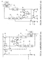
- FIG. 8 is a diagram showing an outline structure of a conventional solenoid drive unit shown in FIG.2 of the aforementioned publication.
- a solenoid drive unit 80 is constituted by an N-channel type MOS transistor (hereinafter referred to as NMOS) 81, a battery 82, a control circuit 83, a diode 84, a solenoid 85, a resistance 86, an amplifier 87, a resistance 88, and a capacitor 89.
- the solenoid drive unit 80 passes a current to a coil of the solenoid 85, and drives the solenoid 85, by exciting the current.
- a drain of the NMOS 81 is connected to a positive electrode of the battery 82.
- a gate of the NMOS 81 is connected to the control circuit 83.
- a source of the NMOS 81 is connected to a cathode of the diode 84 and one end 85a of the solenoid 85.
- a negative electrode of the battery 82 is connected to a ground.
- the control circuit 83 provides a control signal S83 to the gate of the NMOS 81.
- An anode of the diode 84 is connected to the ground.
- Another end 85b of the solenoid 85 is connected to one end of the resistance 86.
- the other end of the resistance 86 is connected to the ground.
- the resistance 86 is a conversion circuit that converts a current that passes through the solenoid 85 to a corresponding voltage. Both ends of the resistance 86 are connected to a positive input terminal (+) and a negative input terminal (-) of the amplifier 87.
- An output terminal of the amplifier 87 is connected to one end of the resistance 88.
- the other end of the resistance 88 is connected to one electrode of the capacitor 89.
- the other electrode of the capacitor 89 is connected to the ground.
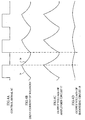
- FIGS. 9A to D are wave form diagrams for describing the operation of the solenoid drive unit 80 in FIG. 8. Operation of the solenoid drive unit 80 will be described with reference to FIG. 9.
- control circuit 83 provides a control signal S83 that repeats a high level (hereinafter referred to as "H”) and a low level (hereinafter referred to as "L”) to the gate of the NMOS 81.
- H high level
- L low level
- the NMOS 81 When the control signal S83 is "H", the NMOS 81 is turned on, and connects one end 85a of the solenoid to the positive electrode of the battery 82. By this, a power source current I 1 passes through the negative electrode of the battery 82 via the positive electrode of the battery 82, the resistance 86, and the ground.
- the amplifier 87 amplifies the difference of voltage of the voltage input to the negative input terminal and the voltage input to the positive input terminal, and outputs a voltage signal 87 that pulsates, as shown in FIG. 9C.
- the smoothing circuit that is constituted by the resistance 88 and the capacitor 89, smoothes and outputs, as shown in FIG. 9D, the voltage signal S87 that the amplifier 87 outputs.
- the smoothed voltage signal S87 output from the smoothing circuit is for example, fed back to the control circuit 83.
- the control circuit 83 changes the duty ratio of the control signal S83, based on the smoothed voltage signal fed back from the smoothing circuit. Namely, the control circuit 83 carries out PWM (Pulse Width Modulation) control. By this, the current that passes through the solenoid 85 is optimized.
- PWM Pulse Width Modulation
- the output of the smoothing circuit is for example, A/D converted, and provided to a processor for vehicle control, which is not shown in the drawings.
- the conventional solenoid drive unit 80 has the problems of below.
- the NMOS 81 witch is a switching element, and the resistance 86, which is a conversion circuit, both generate heat, because a current for driving solenoid 85 passes through. Therefore, the NMOS 81 and the resistance 86 are embedded in an Electronic Control Unit (ECU) as different components.
- ECU Electronic Control Unit
- the temperature in the ECU becomes uneven, and because temperature of each component varies, it is difficult to detect a current (a current that passes through the solenoid 85) accurately.
- a component for temperature correction which is not shown in the drawings, is placed in the ECU. Therefore, the number of components increases, and low-cost of the ECU is difficult. Because the solenoid drive unit is constituted by a plurality of components, miniaturization of the ECU is also difficult.
- the present invention has been made in consideration of the above, and an object of the present invention is to provide a current detection circuit and/or an actuator drive unit, which makes a highly accurate current detection possible, without needing components for temperature correction.
- Another object of the present invention is to provide a current detection circuit and/or an actuator drive unit that has few components.
- Still another object of the present invention is to provide a highly reliable temperature detection circuit and/or a solenoid drive unit.
- a current detection circuit comprises: a conversion circuit (16), which generates, when a current, that is a detection target, passes there through, an electronic signal corresponding to the current that passes; and an amplifier circuit (17), which amplifies the electronic signal generated by the conversion circuit (16), wherein the conversion circuit (16) and the amplifier circuit (17) are formed on a common substrate (100).
- the current detection circuit may further comprise a switching element (11) that connects a power source (12) and an actuator (15), which is a drive target, on an off, wherein: the conversion circuit (16) may be constituted by a circuit that generates an electronic signal that corresponds to a current that passes through the actuator (15) by the connection therewith being switched on and off, by the switching on and off of the switching element (11); the amplifier circuit (17) may amplify the electronic signal that corresponds to the current that passes through the actuator (15), which the conversion circuit (16) outputs, and the switching element (11), the conversion circuit (16), and the amplifier circuit (17) may be formed on a common substrate (100).
- the conversion circuit (16) may be constituted by a circuit that generates an electronic signal that corresponds to a current that passes through the actuator (15) by the connection therewith being switched on and off, by the switching on and off of the switching element (11)
- the amplifier circuit (17) may amplify the electronic signal that corresponds to the current that passes through the actuator (15), which the conversion circuit (16
- the conversion circuit (16) may be constituted by a plurality of conversion elements (16 1 to 16n) that convert the current that passes through the actuator (15) to a voltage, and may generate the electronic signal.
- the plurality of conversion elements (16 1 to 16n) that constitute the conversion circuit (16) may be formed diffused to the substrate (100).
- the plurality of conversion elements (16 1 to 16n) may be constituted by resistive elements.
- the amplifier circuit (17) may comprise a plurality of gain setting circuits (21 to 23) that set the gain of the amplifier circuit (17).
- the plurality of gain setting circuits (21 to 23) may be formed diffused to the substrate (100).
- Each of the plurality of gain setting circuits (21 to 23) may be constituted by a plurality of resistive elements.
- the conversion circuit (16) may be constituted by a plurality of conversion elements (16 1 to 16n) that convert the current that passes through the actuator (15) to a voltage, and may generate the electronic signal;
- the amplifier circuit (17) may comprise a plurality of gain setting circuits (21 to 23) that set the gain of the amplifier circuit (17), and the plurality of gain setting circuits (21 to 23) may be formed close to the conversion elements (16 1 to 16n) of the substrate (100).
- Each of the plurality of gain setting circuits (21 to 23) may be constituted by a plurality of elements, and the plurality of elements and the plurality of conversion elements that constitute the plurality of gain setting circuits (21 to 23) may be formed diffused to the substrate (100).
- the plurality of conversion elements (16 1 to 16n) and the plurality of gain setting circuits (21 to 23) may be placed at a thermally close position.
- the plurality of gain setting circuits (21 to 23) may be constituted by resistive circuits.
- the substrate (100) may be formed by a semiconductor substrate.
- the amplifier circuit (17) may comprise gain setting circuits (21 to 23), the gain changing in accordance with the attribute of the gain setting circuits (21 to 23), and each of the conversion circuit (16) and the gain setting circuits (21 to 23) may be constituted by a plurality of elements, wherein the plurality of elements that constitute the conversion circuit (16) and the plurality of elements that constitute the gain setting circuits (21 to 23) are placed close to each other.
- the amplifier circuit (17) may comprise gain setting circuits (21 to 23), the gain changing in accordance with the attribute of the gain setting circuits (21 to 23), and each of the conversion circuit (16) and the gain setting circuits (21 to 23) may be constituted by a plurality of elements, wherein at least one part of elements that constitute the gain setting circuits (21 to 23) is arranged in between the elements that constitute the conversion circuit (16).
- the conversion circuit (16) may generate heat by the current passing through;
- the amplifier circuit (17) may comprise gain setting circuits (21 to 23), the gain changing in accordance with the attribute of the gain setting circuits (21 to 23), and each of the conversion circuit (16) and the gain setting circuits (21 to 23) may be constituted by a plurality of elements, and may be placed so that the elements that constitute the conversion circuit (16) and the elements that constitute the gain setting circuits (21 to 23) are heated by the heat from the conversion circuit (16).
- the plurality of elements that constitute the conversion circuit (16) and the gain setting circuits (21 to 23) may be placed so that the temperature of the elements that constitute gain setting circuits (21 to 23) rises in accordance with the rise of temperature of the elements that structure the conversion circuit (16), and the temperature of elements that constitute gain setting circuits falls, in accordance with the fall of temperature of the elements that structure the conversion circuit (16).
- Each of the conversion circuit (16) and the plurality of gain setting circuits (21 to 23) may be constituted by a plurality of resistive elements.
- an actuator drive unit comprises the current detection circuit according to the first aspect, which further includes a switching element (11) that connects a power source (12) and an actuator (15), which is a drive target, on an off, in response to a control signal, and a control circuit (13), which provides the control signal to the switching element (11) in accordance with the output of the amplifier circuit (17), wherein: the conversion circuit (16) generates an electronic signal that corresponds to a current that passes through the actuator (15) by the connection therewith being switched on and off, by the switching on and off of the switching element (11), and the amplifier circuit (17) amplifies the electronic signal that corresponds to the current that passes through the actuator (15), which the conversion circuit (16) outputs.
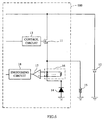
- a solenoid drive unit 10 is constituted by an N-channel MOS transistor (hereinafter referred to as NMOS) 11, a power source 12, a control circuit 13, a diode 14, a solenoid 15, a conversion circuit 16, an amplifier circuit 17, and a smoothing circuit 18.
- NMOS N-channel MOS transistor
- the NMOS 11, the control circuit 13, the diode 14, the conversion circuit 16, the amplifier circuit 17, and the smoothing circuit 18 are formed on a common semiconductor substrate 100.
- the NMOS 11 functions as a current switch, and the drain thereof is connected to the positive electrode of the power source 12.
- the gate of the NMOS 11 is connected to the control circuit 13.
- the source of the NMOS 11 is connected to a cathode of the diode 14 and one end 15a of a coil of the solenoid 15.
- a power source current I 1 from the power source 12 is passed through the coil of the solenoid 15.
- the negative electrode of the battery 12 is connected to a ground.
- the control circuit 13 provides a control signal SC to the gate of the NMOS 11, and turns on/off the NMOS 11.
- the anode of the diode 14 is connected to the ground.
- the cathode of the diode 14 is connected to a connection point of the source of the NMOS 11 and one end 15a of the coil of the solenoid 15.
- the diode 14 passes through from the ground to the one end 15a of the solenoid 15, a regenerative current I 0 , which occurs by counter electromotive force generated in the coil of the solenoid 15 when the NMOS 11 is turned off.
- the conversion circuit 16 is constituted by a plurality of resistor elements 16 1 to 16n that are connected in parallel, in between another end 15b of the coil of the solenoid 15, and the ground.
- the conversion circuit 16 converts to a voltage corresponding to a current passing thought the solenoid 15.
- the converter 16 can produce physically one resistor element having an equal capacity (value of resistance, current capacity, etc.).
- the conversion circuit 16 is constituted by a parallel circuit of a plurality of resistor elements.
- FIGS. 2A and B are drawings showing an example of a structure of the amplifier circuit 17.
- an amplifier circuit AA shown in FIG. 2A, an amplifier circuit AB shown in FIG. 2B, or an amplifier circuit that has combined the amplifier circuit AA and the amplifier circuit AB is used.
- a resistive circuit 21 that is constituted by a plurality of resistor elements that are serially connected, a resistive circuit 22 that is constituted by a plurality of resistor elements that are serially connected, and a resistive circuit 23 that is constituted by a plurality of resistor elements that are serially connected, are provided on the amplifier circuit AA, amplifier circuit AB, or the amplifier circuit that has combined the amplifier circuit AA and the amplifier circuit AB.
- the resistive circuits 21 to 23 are for adjusting the gain (amplification factor) of the amplifier circuit 17.
- the conversion circuit 16 is constituted by a combination of a plurality of resistor elements.
- one end of the resistive circuit 21 is connected to a positive input terminal (+).
- One end of the resistive circuit 22 is connected to one end of the resistive circuit 23, and the other end of the resistive circuit 23 is connected to a negative input terminal (-) of the resistive circuit 23.
- Four PNP-type transistors 30, 31, 32, and 33 wherein an emitter is commonly connected to the power source, and a current source 34, are set in the amplifier circuit AA.
- the base of the transistor 30 is connected to the base and the collector of the transistor 31.
- the collector of the transistor 30 is connected to the collector of an NPN-type transistor 35, and the emitter of the transistor 35 is connected to another end of the resistive circuit 21.
- the current source 34 is connected to a base of the transistor 35, a collector and a base of the NPN-type transistor 36, a collector and a base of the NPN-type transistor 37, and a base of the NPN-type transistor 38.
- An emitter of the transistor 36 is connected to another end of the resistive circuit 21.
- An emitter of the transistors 37 and 38 are connected to another end of the resistive circuit 22.
- a collector of the transistor 31 is connected to a collector of the transistor 38.
- Bases of the transistors 32 and 33 are connected to a collector of the transistor 32.
- a collector of the transistor 32 is connected to a collector of a PNP-type transistor 40 wherein a base thereof is connected to a collector of the transistor 30.
- An emitter of the transistor 40 is connected at a connection point of the resistive circuit 22 and the resistive circuit 23.
- a collector of the transistor 33 is connected to one end of a resistance 41.
- the other end of the resistance 41 is grounded.
- the transistors 30, 31, 35 to 38, and the current source 34 become a constant current source circuit, and passes a current through to the transistor 40, so that the current that passes through the resistive circuit 21, and the current that passes through the resistive circuit 22 are equal.
- the current that goes through the transistor 40 corresponds to the regenerative circuit I 0 .
- the transistor 33 passes through a current that is proportional to the current that passes through the transistor 40, to the resistance 41.
- the resistance 41 generates a voltage corresponding to the regenerative circuit I 0 , as a current detection signal.
- the amplifier circuit AB comprises two NPN-type transistors 45 and 46 that each have emitters grounded, and a current source 47.
- a base of the transistor 45 is connected to a base and collector of the transistor 46.
- a collector of the transistor 45 is connected to a collector of the PNP-type transistor 48.
- An emitter of the transistor 48 is connected to one end of the resistive circuit 21.
- the current source 47 is connected to a base of the transistor 48, and at the same time to a collector and a base of the PNP-type transistor 49, a collector and a base of the PNP-type transistor 50, and a base of the PNP-type transistor 51.
- An emitter of the transistor 49 is connected to an emitter of the transistor 48.
- a collector of the transistor 51 is connected to a collector of the transistor 46.
- An emitter of the transistor 51 and an emitter of the transistor 50 are connected to one end of the resistive circuit 23.
- the other end of the resistive circuit 23 is connected to one end of the resistive circuit 22, and the other end of the resistive circuit 22 is connected to a positive input terminal (+).
- the other end of the resistive circuit 21 is connected to a negative input terminal (-).
- an emitter of the PNP-type transistor 52 is connected.
- a base of the transistor 52 is connected to a collector of the transistor 48, and a collector of the transistor 52 is connected to one end of a resistance 53. The other end of the resistance 53 is grounded.
- the smoothing circuit 18 is constituted by a resistance 18a wherein one end is connected to an output terminal of the amplifier circuit 17, and a capacitor 18b which is connected in between another end of a resistance 17a and a ground.
- the connection point of the resistance 18a and the capacitor 18b forms the output terminal of the smoothing circuit 17, and smoothes the output signal of the amplifier circuit 17.
- FIG. 3 is a diagram for describing an example of a layout of the solenoid drive unit 10.
- the NMOS 11 as a switching element, and the peripheral circuits including the control circuit 13, the conversion circuit 16, the amplifier circuit 17, and the smoothing circuit 18, are for example, as shown in FIG. 3, laid out in a semiconductor substrate 100.
- Resistor elements 16 1 to 16n that structure the conversion circuit 16 are connected parallel at the semiconductor substrate 100, and are arranged dispersed.
- the resistive circuits 21 to 23 that determine the gain of the amplifier circuit 17 are arranged between the dispersed resistor elements 16 1 to 16n.
- the resistive circuits 21 to 23 also receive effect of heat equally, by structuring each of the resistive circuits 21 to 23 with a plurality of resistor elements, and arranging them in between the resistor elements 16 1 to 16n of the conversion circuit 16. In other words, the resistive circuits 21 to 23 and the conversion circuit 16 are closely combined thermally.
- the conversion circuit 16 generates heat by a current that passes through the solenoid 15, the temperature of the resistive circuits 21 to 23 rise in accordance with the amount of generated heat thereof. Therefore, a highly accurate detection result is obtained without the need to install components and elements for temperature correction, to maintain the gain of the amplifier circuit 17 suitably.
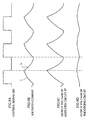
- FIGS. 4A to D are wave form charts for describing operations of the solenoid drive unit 10 in FIG. 1.
- the control circuit 13 provides a control signal SC, whose level is repeated between a high level (hereinafter referred to as "H” ) and a low level (hereinafter referred to as "L”), as shown in FIG. 4A, to the gate of the NMOS 11, for driving the NMOS 11 to switch it on and off.
- SC control signal
- the NMOS 11 When the control signal SC is "H", the NMOS 11 is at an on state, and the NMOS 11 passes the power source current I 1 , shown in FIG. 4B, to the solenoid 15 from the power source 12.
- the power source current I 1 that passed through the solenoid 15 passes through to the ground, being divided to the resistor elements 16 1 to 16n in the conversion circuit 16.
- the NMOS 11 When the control signal is "L", the NMOS 11 is at an off state, and the power source 12 and the solenoid 15 are disconnected.
- the voltage of the other end 15a of the solenoid 15, where one end 15b is connected to the ground reduces by a counterelectromotive force, and forward voltage is applied to the diode 14.
- the diode 14, which is applied to the forward voltage becomes a conducting state, and passes through the regenerative current I 0 shown in FIG. 4B, from the ground to the other end 15a of the solenoid 15.
- the current I 0 that passed through the solenoid 15 passes through the ground, being divided to the resistor elements 16 1 to 16n in the conversion circuit 16.
- the solenoid 15 is driven by the power source current I 1 and the regenerative current I 0 .
- the amplifier circuit 17 When applying an amplifier circuit that synthesized the amplifier circuit AA in FIG. 2A and the amplifier circuit AB in FIG. 2B, as the amplifier circuit 17, the amplifier circuit 17 amplifies the voltage signal corresponding to the currents I 0 and I 1 that the conversion circuit 16 generates, and outputs a voltage that pulsates, such as shown in FIG. 4C.
- the output voltage of the amplifier circuit 17 is output to the smoothing circuit 18, as the current detection signal.
- the gain of the current detection signal that the amplifier circuit 17 outputs, is set in the resistive circuits 21 to 23.
- the smoothing circuit 18 smoothes the output voltage of the amplifier circuit 17, such as shown in FIG. 4D.
- the output of the smoothing circuit 18 is for example, A/D converted, and provided to processors for vehicle control, which is not shown in the drawings.
- the control circuit 13 controls the control signal, in accordance with the level of the signal that the smoothing circuit 18 outputs. For example, the control circuit 13 controls the frequency of the pulse of the control signal SC, or controls the pulse width, so that the signal level of the output signal of the smoothing circuit 18 becomes a desired level.
- the conversion circuit 16 is constituted by a plurality of resistor elements 16 1 to 16n, and are arranged dispersed. By this, the generation area of heat becomes a wide range. Also, by each of the resistive circuits 21 to 23 being constituted by a plurality of resistor elements 16 1 to 16n, and arranging them in between the resistor elements 16 1 to 16n, the effect of heat can be equally received. In other words, the resistive circuits 21 to 23 and the conversion circuit 16 are closely combined thermally. When the conversion circuit 16 generates heat by a current that passes through the solenoid 15, the temperature of the resistive circuits 21 to 23 rise in accordance with the amount of generated heat thereof.
- the solenoid drive unit 10 of the present embodiment has the advantages of below.
- the NMOS 11, the control circuit 13, the conversion circuit 16, the amplifier circuit 17, and the smoothing circuit 18 are formed on the common semiconductor substrate 100, using a semiconductor device manufacturing process, the number of components can be reduced.
- the NMOS 11, the control circuit 13, the conversion circuit 16, the amplifier circuit 17, and the smoothing circuit 18 are formed on the common semiconductor substrate 100, temperature distribution can be made uniform, and a highly accurate current detection is possible, without the need to install components for temperature correction.
- the conversion circuit 16 is constituted by the plurality of resistor elements 16 1 to 16n, and further arranged dispersed, heat generating area spreads, and the temperature of the semiconductor substrate 100 can be made even more uniform.
- each of the resistive circuits 21 to 23 is constituted by a plurality of resistor elements, and are placed in between the plurality of resistor elements 16 1 to 16n in the conversion circuit 16, the thermal coupling of the resistive circuits 21 to 23 and the conversion circuit 16 improves, and accuracy of current detection can be highly maintained.
- the present invention is not limited to the above embodiment, and various modification is possible. As an example of modification, there is an embodiment as below.
- the resistive circuits 21 to 23 in the amplifier circuit 17 and the plurality of resistor elements 16 1 to 16n are constituted by pure resistance.
- These resistor elements for example, diffuse impurities in the semiconductor substrate, and are constituted by a region of an arbitrary impurity concentration (electric conductivity).
- an insulating film may be placed on the semiconductor substrate, and the resistor elements may be constituted by a semiconductor or a resistance layer formed on the insulating film.
- the resistor elements do not have to be constituted by pure resistance, and may be constituted by a MOS transistor which has a predetermined voltage applied to the gate thereof, or a bipolar transistor which has an arbitrary voltage applied to the base thereof. Namely, an arbitrary circuit element may be applied, as long as it functions as an equivalent resistance.
- FIGS. 5 and 6 are each diagrams showing an example of a modification of the solenoid drive unit 10.
- the solenoid 15 can be current driven.
- the smoothing circuit 18 may be changed to a sample and hold circuit 19 that samples the output signal of the amplifier circuit 17 at a set timing, and retains the output signal.
- the conversion circuit 16 is constituted by the parallel circuit of the plurality of resistor elements.
- the conversion circuit 16 may be constituted by a series circuit of a plurality of resistor elements.
- Each of the resistive circuits 21 to 23 for determining the gain is constituted by the series circuit of the plurality of resistor elements.
- each of the resistive circuits 21 to 23 may be constituted by a parallel circuit of a plurality of resistor elements.
- the arrangements of the conversion circuit 16 and the resistive circuits 21 to 23 are also arbitrary, as long as the heat generated by the conversion circuit 17 is transmitted to the resistive circuits 21 to 23, and the variation of the resistance of the resistor elements that constitute the conversion circuit 16 can follow the variation of the resistance of the resistive circuits 21 to 23.
- the resistor elements that constitute the conversion circuit 16 may be arranged in a loop-shape, and the resistive circuits 21 to 23 may be placed in the loop.
- the conversion circuit 16 may be placed in one place, and the resistive circuits 21 to 23 may be arranged closely around the vicinity thereof.
- a current subject to detection is not limited to a solenoid drive current, and the present invention can be applied for detection of an arbitrary drive current of an actuator, such as for example, a pulse motor, and a stepping motor, etc.
- the present invention can be applied to an area of industry, which uses actuator drive circuits.
Landscapes
- Physics & Mathematics (AREA)
- General Physics & Mathematics (AREA)
- Electronic Switches (AREA)
- Measurement Of Current Or Voltage (AREA)
- Control Of Voltage And Current In General (AREA)
Abstract
Description
Claims (19)
- A current detection circuit comprising:a conversion circuit (16), which generates, when a current, that is a detection target, passes there through, an electronic signal corresponding to the current that passes; andan amplifier circuit (17), which amplifies the electronic signal generated by said conversion circuit (16), whereinsaid conversion circuit (16) and said amplifier circuit (17) are formed on a common substrate (100).
- The current detection circuit according to claim 1, further comprising:a switching element (11) that connects a power source (12) and an actuator (15), which is a drive target, on an off, wherein:said conversion circuit (16) is constituted by a circuit that generates an electronic signal that corresponds to a current that passes through the actuator (15) by the connection therewith being switched on and off, by the switching on and off of said switching element (11);said amplifier circuit (17) amplifies the electronic signal that corresponds to the current that passes through the actuator (15), which the conversion circuit (16) outputs, andsaid switching element (11), said conversion circuit (16), and said amplifier circuit (17) are formed on a common substrate (100).
- The current detection circuit according to claim 2, wherein:said conversion circuit (16) is constituted by a plurality of conversion elements (161 to 16n) that convert the current that passes through said actuator (15) to a voltage, and generates said electronic signal.
- The current detection circuit according to claim 3, wherein:the plurality of conversion elements (161 to 16n) that constitute said conversion circuit (16) are formed diffused to said substrate (100).
- The current detection circuit according to claim 3, wherein:the plurality of conversion elements (161 to 16n) are constituted by resistive elements.
- The current detection circuit according to claim 3, wherein:said amplifier circuit (17) comprises a plurality of gain setting circuits (21 to 23) that set the gain of the amplifier circuit (17).
- The current detection circuit according to claim 6, wherein:the plurality of gain setting circuits (21 to 23) are formed diffused to said substrate (100).
- The current detection circuit according to claim 7, wherein:each of the plurality of gain setting circuits (21 to 23) is constituted by a plurality of resistive elements.
- The current detection circuit according to claim 7, wherein:said conversion circuit (16) is constituted by a plurality of conversion elements (161 to 16n) that convert the current that passes through said actuator (15) to a voltage, and generates said electronic signal;said amplifier circuit (17) comprises a plurality of gain setting circuits (21 to 23) that set the gain of the amplifier circuit (17), andsaid plurality of gain setting circuits (21 to 23) are formed close to the conversion elements (161 to 16n) of said substrate (100).
- The current detection circuit according to claim 9, wherein:each of the plurality of gain setting circuits (21 to 23) is constituted by a plurality of elements, andthe plurality of elements (161 to 16n) and said plurality of conversion elements that constitute the plurality of gain setting circuits (21 to 23) are formed diffused to said substrate (100).
- The current detection circuit according to claim 8, wherein:the plurality of conversion elements (161 to 16n) and the plurality of gain setting circuits (21 to 23) are placed at a thermally close position.
- The current detection circuit according to claim 7, wherein:said plurality of gain setting circuits (21 to 23) are constituted by resistive circuits.
- The current detection circuit according to claim 1, wherein:said substrate (100) is formed by a semiconductor substrate.
- The current detection circuit according to claim 1, wherein:said amplifier circuit (17) comprises gain setting circuits (21 to 23), the gain changing in accordance with the attribute of the gain setting circuits (21 to 23), andeach of said conversion circuit (16) and said gain setting circuits (21 to 23) is constituted by a plurality of elements, wherein the plurality of elements that constitute said conversion circuit (16) and the plurality of elements that constitute said gain setting circuits (21 to 23) are placed close to each other.
- The current detection circuit according to claim 1, wherein:said amplifier circuit (17) comprises gain setting circuits (21 to 23), the gain changing in accordance with the attribute of the gain setting circuits (21 to 23), andeach of said conversion circuit (16) and said gain setting circuits (21 to 23) is constituted by a plurality of elements, wherein at least one part of elements that constitute said gain setting circuits (21 to 23) is arranged in between the elements that constitute said conversion circuit (16).
- The current detection circuit according to claim 1, wherein:said conversion circuit (16) generates heat by said current passing through;said amplifier circuit (17) comprises gain setting circuits (21 to 23), the gain changing in accordance with the attribute of the gain setting circuits (21 to 23), andeach of said conversion circuit (16) and said gain setting circuits (21 to 23) is constituted by a plurality of elements, and are placed so that the elements that constitute said conversion circuit (16) and the elements that constitute said gain setting circuits (21 to 23) are heated by the heat from said conversion circuit (16).
- The current detection circuit according to claim 16, wherein:the plurality of elements that constitute said conversion circuit (16) and said gain setting circuits (21 to 23) are placed so that the temperature of the elements that constitute gain setting circuits (21 to 23) rises in accordance with the rise of temperature of the elements that structure the conversion circuit (16), and the temperature of elements that constitute gain setting circuits (21 to 23) falls, in accordance with the fall of temperature of the elements that structure the conversion circuit (16).
- The current detection circuit according to claim 17, wherein:each of the conversion circuit (16) and the plurality of gain setting circuits (21 to 23) is constituted by a plurality of resistive elements.
- An actuator drive unit that comprises the current detection circuit according to claim 1, which further includes
a switching element (11) which connects a power source (12) and an actuator (15), that is a drive target, on an off, in response to a control signal, and
a control circuit (13), which provides said control signal to said switching element (11) in accordance with the output of said amplifier circuit (17), wherein:said conversion circuit (16) generates an electronic signal that corresponds to a current that passes through the actuator (15) by the connection therewith being switched on and off, by the switching on and off of said switching element (11), andsaid amplifier circuit (17) amplifies the electronic signal that corresponds to the current that passes through the actuator (15), which the conversion circuit (16) outputs.
Applications Claiming Priority (3)
| Application Number | Priority Date | Filing Date | Title |
|---|---|---|---|
| JP2001368125 | 2001-12-03 | ||
| JP2001368125 | 2001-12-03 | ||
| PCT/JP2002/012667 WO2003048790A1 (en) | 2001-12-03 | 2002-12-03 | Current detecting circuit and actuator driving apparatus |
Publications (3)
| Publication Number | Publication Date |
|---|---|
| EP1452879A1 true EP1452879A1 (en) | 2004-09-01 |
| EP1452879A4 EP1452879A4 (en) | 2009-04-15 |
| EP1452879B1 EP1452879B1 (en) | 2010-09-15 |
Family
ID=19177760
Family Applications (1)
| Application Number | Title | Priority Date | Filing Date |
|---|---|---|---|
| EP02783748A Expired - Lifetime EP1452879B1 (en) | 2001-12-03 | 2002-12-03 | Current detecting circuit and actuator driving apparatus |
Country Status (5)
| Country | Link |
|---|---|
| US (1) | US7423857B2 (en) |
| EP (1) | EP1452879B1 (en) |
| JP (2) | JP4124125B2 (en) |
| DE (1) | DE60237705D1 (en) |
| WO (1) | WO2003048790A1 (en) |
Cited By (3)
| Publication number | Priority date | Publication date | Assignee | Title |
|---|---|---|---|---|
| EP2169412A1 (en) * | 2008-09-25 | 2010-03-31 | Ilumab AB | Electrical current measurement arrangement |
| DE102011083307A1 (en) * | 2011-09-23 | 2013-03-28 | Continental Automotive Gmbh | Device for measuring a battery current |
| US12529243B2 (en) | 2015-04-14 | 2026-01-20 | Hanchett Entry Systems, Inc. | Power controller for a door lock and method of conserving power |
Families Citing this family (9)
| Publication number | Priority date | Publication date | Assignee | Title |
|---|---|---|---|---|
| JP4501555B2 (en) * | 2004-06-30 | 2010-07-14 | Tdk株式会社 | Current detection circuit |
| JP4556754B2 (en) * | 2005-04-20 | 2010-10-06 | 株式会社デンソー | Inductive load drive |
| JP4600180B2 (en) * | 2005-06-27 | 2010-12-15 | 株式会社日立製作所 | Semiconductor circuit using field effect type power semiconductor element |
| JP4513920B2 (en) * | 2008-06-19 | 2010-07-28 | 株式会社デンソー | Constant current control circuit |
| US8816722B2 (en) * | 2010-09-13 | 2014-08-26 | Semiconductor Energy Laboratory Co., Ltd. | Current detection circuit |
| CN102768299A (en) * | 2012-07-27 | 2012-11-07 | 北京经纬恒润科技有限公司 | High-side current sampling circuit |
| CN108780691B (en) * | 2016-03-30 | 2021-06-25 | 爱信艾达株式会社 | Linear Solenoid Drive |
| DE102017219633B3 (en) | 2017-11-06 | 2019-02-28 | Conti Temic Microelectronic Gmbh | Method for checking the plausibility of measurements of an actuator current and use of the method |
| JP7259632B2 (en) * | 2019-08-09 | 2023-04-18 | Tdk株式会社 | current sensor |
Family Cites Families (15)
| Publication number | Priority date | Publication date | Assignee | Title |
|---|---|---|---|---|
| DE2501824A1 (en) * | 1975-01-17 | 1976-07-22 | Krasnod Sawod Elektroismeritel | Temp. compensated printed resistor - has series-parallel arm network with one arm section of high temp. coeffn. |
| US4078215A (en) * | 1976-11-26 | 1978-03-07 | Altec Corporation | Electronic filter circuit |
| JPS58173921A (en) * | 1982-04-06 | 1983-10-12 | Nec Corp | Microwave communication device |
| JPS63163284A (en) * | 1986-12-26 | 1988-07-06 | Fuji Electric Co Ltd | Overcurrent detecting circuit |
| JPS63190974A (en) * | 1987-01-29 | 1988-08-08 | Horikawa Jiro | Vulcanized rubber packing |
| JP2994649B2 (en) * | 1988-08-05 | 1999-12-27 | 株式会社アドバンテスト | Voltage applied current measuring device with automatic calibration function |
| JPH02128964A (en) | 1988-11-10 | 1990-05-17 | Mitsubishi Automob Eng Co Ltd | Cylinder device |
| US5498984A (en) | 1994-09-30 | 1996-03-12 | Maxim Integrated Products | High side, current sense amplifier using a symmetric amplifier |
| JP3085132B2 (en) * | 1995-03-02 | 2000-09-04 | 本田技研工業株式会社 | Control device for pulse width modulation solenoid |
| JPH09130004A (en) * | 1995-11-01 | 1997-05-16 | Yazaki Corp | Overcurrent detection circuit and overcurrent detection IC using the same |
| JPH10256915A (en) * | 1997-03-11 | 1998-09-25 | Mitsubishi Electric Corp | Digital / analog conversion circuit |
| DE59802861D1 (en) | 1997-10-17 | 2002-02-28 | Siemens Ag | CIRCUIT ARRANGEMENT FOR REGULATING THE CURRENT SUPPLIED TO AN ELECTROMECHANICAL COMPONENT IN A MOTOR VEHICLE |
| GB9813668D0 (en) | 1998-06-25 | 1998-08-26 | Sentec Ltd | Printed circuit board current sensor |
| US6336448B1 (en) * | 1999-08-20 | 2002-01-08 | Fuji Electric Co., Ltd. | Ignition semiconductor device |
| US6892443B2 (en) * | 2002-11-25 | 2005-05-17 | Vishay Intertechnology | Method of manufacturing a resistor |
-
2002
- 2002-12-03 WO PCT/JP2002/012667 patent/WO2003048790A1/en not_active Ceased
- 2002-12-03 DE DE60237705T patent/DE60237705D1/en not_active Expired - Lifetime
- 2002-12-03 US US10/495,015 patent/US7423857B2/en not_active Expired - Lifetime
- 2002-12-03 JP JP2003549934A patent/JP4124125B2/en not_active Expired - Lifetime
- 2002-12-03 EP EP02783748A patent/EP1452879B1/en not_active Expired - Lifetime
-
2008
- 2008-03-31 JP JP2008093470A patent/JP4737217B2/en not_active Expired - Lifetime
Cited By (4)
| Publication number | Priority date | Publication date | Assignee | Title |
|---|---|---|---|---|
| EP2169412A1 (en) * | 2008-09-25 | 2010-03-31 | Ilumab AB | Electrical current measurement arrangement |
| DE102011083307A1 (en) * | 2011-09-23 | 2013-03-28 | Continental Automotive Gmbh | Device for measuring a battery current |
| US9360500B2 (en) | 2011-09-23 | 2016-06-07 | Continental Automotive Gmbh | Device for measuring a battery current |
| US12529243B2 (en) | 2015-04-14 | 2026-01-20 | Hanchett Entry Systems, Inc. | Power controller for a door lock and method of conserving power |
Also Published As
| Publication number | Publication date |
|---|---|
| EP1452879A4 (en) | 2009-04-15 |
| JPWO2003048790A1 (en) | 2005-04-14 |
| WO2003048790A1 (en) | 2003-06-12 |
| EP1452879B1 (en) | 2010-09-15 |
| JP4124125B2 (en) | 2008-07-23 |
| US7423857B2 (en) | 2008-09-09 |
| DE60237705D1 (en) | 2010-10-28 |
| US20050002143A1 (en) | 2005-01-06 |
| JP4737217B2 (en) | 2011-07-27 |
| JP2008216262A (en) | 2008-09-18 |
Similar Documents
| Publication | Publication Date | Title |
|---|---|---|
| JP4737217B2 (en) | Current detection circuit | |
| US7550959B2 (en) | Power supply device and switching power supply device | |
| JP2003070230A (en) | Power converter with shunt resistor | |
| JP4736668B2 (en) | Signal detection device for load driving device | |
| JP3526245B2 (en) | Load drive circuit | |
| US7586367B2 (en) | Current sensor device | |
| JPH075225A (en) | Circuit structure for monitoring drain current of metal / oxide / semiconductor field effect transistor | |
| TWI422281B (en) | Led controller and method therefor | |
| CN111464029A (en) | Current sensing controller for DC-DC converter | |
| CN110545032B (en) | A power transistor module and voltage conversion circuit with integrated startup function | |
| US7430102B2 (en) | Pulse width modulated servo clutch driver | |
| JP2000112541A (en) | Circuit for detecting load current and amplifier circuit for detecting current | |
| CN119906406A (en) | Intelligent electronic switches, chips and devices with integrated diode functions | |
| US4987384A (en) | High frequency amplifier | |
| CN114928244B (en) | Line loss compensation correction method and circuit based on output current | |
| US10566123B2 (en) | Linear solenoid driving device | |
| US6535067B1 (en) | Power saturation control of class C bipolar amplifiers | |
| TW201240311A (en) | Method for scaling a drive signal and circuit therefor | |
| JP3457151B2 (en) | Coil drive circuit | |
| US20260100573A1 (en) | Driver circuit with real-time thermal management | |
| JPH05235253A (en) | Semiconductor device | |
| JP2000244291A (en) | Semiconductor relay | |
| JP2003270275A (en) | Current detection circuit | |
| JPH118119A (en) | Electronic control unit | |
| JP2000114454A (en) | Transistor structure |
Legal Events
| Date | Code | Title | Description |
|---|---|---|---|
| PUAI | Public reference made under article 153(3) epc to a published international application that has entered the european phase |
Free format text: ORIGINAL CODE: 0009012 |
|
| 17P | Request for examination filed |
Effective date: 20040510 |
|
| AK | Designated contracting states |
Kind code of ref document: A1 Designated state(s): AT BE BG CH CY CZ DE DK EE ES FI FR GB GR IE IT LI LU MC NL PT SE SI SK TR |
|
| A4 | Supplementary search report drawn up and despatched |
Effective date: 20090317 |
|
| RIC1 | Information provided on ipc code assigned before grant |
Ipc: G01R 1/20 20060101ALI20090311BHEP Ipc: G01R 19/32 20060101AFI20030619BHEP |
|
| 17Q | First examination report despatched |
Effective date: 20090623 |
|
| GRAP | Despatch of communication of intention to grant a patent |
Free format text: ORIGINAL CODE: EPIDOSNIGR1 |
|
| GRAS | Grant fee paid |
Free format text: ORIGINAL CODE: EPIDOSNIGR3 |
|
| GRAA | (expected) grant |
Free format text: ORIGINAL CODE: 0009210 |
|
| AK | Designated contracting states |
Kind code of ref document: B1 Designated state(s): DE FR GB |
|
| REG | Reference to a national code |
Ref country code: GB Ref legal event code: FG4D |
|
| REF | Corresponds to: |
Ref document number: 60237705 Country of ref document: DE Date of ref document: 20101028 Kind code of ref document: P |
|
| PLBE | No opposition filed within time limit |
Free format text: ORIGINAL CODE: 0009261 |
|
| STAA | Information on the status of an ep patent application or granted ep patent |
Free format text: STATUS: NO OPPOSITION FILED WITHIN TIME LIMIT |
|
| 26N | No opposition filed |
Effective date: 20110616 |
|
| REG | Reference to a national code |
Ref country code: DE Ref legal event code: R097 Ref document number: 60237705 Country of ref document: DE Effective date: 20110616 |
|
| REG | Reference to a national code |
Ref country code: FR Ref legal event code: PLFP Year of fee payment: 14 |
|
| REG | Reference to a national code |
Ref country code: FR Ref legal event code: PLFP Year of fee payment: 15 |
|
| REG | Reference to a national code |
Ref country code: FR Ref legal event code: PLFP Year of fee payment: 16 |
|
| PGFP | Annual fee paid to national office [announced via postgrant information from national office to epo] |
Ref country code: FR Payment date: 20211109 Year of fee payment: 20 Ref country code: GB Payment date: 20211028 Year of fee payment: 20 Ref country code: DE Payment date: 20211102 Year of fee payment: 20 |
|
| REG | Reference to a national code |
Ref country code: DE Ref legal event code: R071 Ref document number: 60237705 Country of ref document: DE |
|
| REG | Reference to a national code |
Ref country code: GB Ref legal event code: PE20 Expiry date: 20221202 |
|
| PG25 | Lapsed in a contracting state [announced via postgrant information from national office to epo] |
Ref country code: GB Free format text: LAPSE BECAUSE OF EXPIRATION OF PROTECTION Effective date: 20221202 |