EP1452628A1 - Copper electroplating method, pure copper anode for copper electroplating, and semiconductor wafer plated thereby with little particle adhesion - Google Patents
Copper electroplating method, pure copper anode for copper electroplating, and semiconductor wafer plated thereby with little particle adhesion Download PDFInfo
- Publication number
- EP1452628A1 EP1452628A1 EP02760809A EP02760809A EP1452628A1 EP 1452628 A1 EP1452628 A1 EP 1452628A1 EP 02760809 A EP02760809 A EP 02760809A EP 02760809 A EP02760809 A EP 02760809A EP 1452628 A1 EP1452628 A1 EP 1452628A1
- Authority
- EP
- European Patent Office
- Prior art keywords
- anode
- electrolytic copper
- copper
- copper plating
- pure
- Prior art date
- Legal status (The legal status is an assumption and is not a legal conclusion. Google has not performed a legal analysis and makes no representation as to the accuracy of the status listed.)
- Withdrawn
Links
Images
Classifications
-
- C—CHEMISTRY; METALLURGY
- C25—ELECTROLYTIC OR ELECTROPHORETIC PROCESSES; APPARATUS THEREFOR
- C25D—PROCESSES FOR THE ELECTROLYTIC OR ELECTROPHORETIC PRODUCTION OF COATINGS; ELECTROFORMING; APPARATUS THEREFOR
- C25D7/00—Electroplating characterised by the article coated
- C25D7/12—Semiconductors
- C25D7/123—Semiconductors first coated with a seed layer or a conductive layer
-
- C—CHEMISTRY; METALLURGY
- C25—ELECTROLYTIC OR ELECTROPHORETIC PROCESSES; APPARATUS THEREFOR
- C25D—PROCESSES FOR THE ELECTROLYTIC OR ELECTROPHORETIC PRODUCTION OF COATINGS; ELECTROFORMING; APPARATUS THEREFOR
- C25D17/00—Constructional parts, or assemblies thereof, of cells for electrolytic coating
- C25D17/001—Apparatus specially adapted for electrolytic coating of wafers, e.g. semiconductors or solar cells
-
- C—CHEMISTRY; METALLURGY
- C25—ELECTROLYTIC OR ELECTROPHORETIC PROCESSES; APPARATUS THEREFOR
- C25D—PROCESSES FOR THE ELECTROLYTIC OR ELECTROPHORETIC PRODUCTION OF COATINGS; ELECTROFORMING; APPARATUS THEREFOR
- C25D17/00—Constructional parts, or assemblies thereof, of cells for electrolytic coating
- C25D17/10—Electrodes, e.g. composition, counter electrode
-
- C—CHEMISTRY; METALLURGY
- C25—ELECTROLYTIC OR ELECTROPHORETIC PROCESSES; APPARATUS THEREFOR
- C25D—PROCESSES FOR THE ELECTROLYTIC OR ELECTROPHORETIC PRODUCTION OF COATINGS; ELECTROFORMING; APPARATUS THEREFOR
- C25D21/00—Processes for servicing or operating cells for electrolytic coating
- C25D21/04—Removal of gases or vapours ; Gas or pressure control
-
- C—CHEMISTRY; METALLURGY
- C25—ELECTROLYTIC OR ELECTROPHORETIC PROCESSES; APPARATUS THEREFOR
- C25D—PROCESSES FOR THE ELECTROLYTIC OR ELECTROPHORETIC PRODUCTION OF COATINGS; ELECTROFORMING; APPARATUS THEREFOR
- C25D3/00—Electroplating: Baths therefor
- C25D3/02—Electroplating: Baths therefor from solutions
- C25D3/38—Electroplating: Baths therefor from solutions of copper
Definitions
- the present invention pertains to an electrolytic copper plating method and a pure copper anode used in such electrolytic copper plating method capable of suppressing the generation of particles such as sludge produced on the anode side within the plating bath upon performing electrolytic copper plating, and in particular capable of preventing the adhesion of particles to a semiconductor wafer, as well as to a semiconductor wafer having low particle adhesion plated with the foregoing method and anode.
- an electrolytic copper plate has been employed for forming copper wiring in a PWB (print wiring board) or the like, in recent years, it is being used for forming copper wiring of semiconductors.
- An electrolytic copper plate has a long history, and it has reached its present form upon accumulating numerous technical advancements. Nevertheless, when employing this electrolytic copper plate for forming copper wiring of semiconductors, a new problem arose which was not found in a PWB.
- phosphorous copper is used as the anode.
- an insoluble anode formed from the likes of platinum, titanium, or iridium oxide is used, the additive within the plating liquid would decompose upon being affected by anodic oxidization, and inferior plating will occur thereby.
- electrolytic copper or oxygen-free copper of a soluble anode a large amount of particles such as sludge is generated from metallic copper or copper oxide caused by the dismutation reaction of monovalent copper during dissolution, and the plating object will become contaminated as a result thereof.
- a black film composed of phosphorous copper or copper chloride is formed on the anode surface due to electrolysis, and it is thereby possible to suppress the generation of metallic copper or copper oxide caused by the dismutation reaction of monovalent copper, and to control the generation of particles.
- a filter cloth referred to as an anode bag is ordinarily used to wrap the anode so as to prevent particles from reaching the plating liquid.
- the present invention aims to provide an electrolytic copper plating method and a pure copper anode used in such electrolytic copper plating method capable of suppressing the generation of particles such as sludge produced on the anode side within the plating bath upon performing electrolytic copper plating, without using phosphorous copper, and in particular capable of preventing the adhesion of particles to a semiconductor wafer, as well as to a semiconductor wafer having low particle adhesion plated with the foregoing method and anode.
- a semiconductor wafer and the like having low particle adhesion can be manufactured stably by improving the electrode material, and suppressing the generation of particles in the anode.
- the present invention provides:
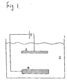
- Fig. 1 is a conceptual diagram of a device used in the electrolytic copper plating method of a semiconductor wafer according to the present invention.
- Fig. 1 is a diagram illustrating an example of the device employed in the electrolytic copper plating method of a semiconductor wafer.
- the copper plating device is equipped with the plating bath 1 containing copper sulfate plating liquid 2.
- a pure copper anode 4 is used as the anode, and, as the cathode, for example, a semiconductor wafer is used as the object of plating.
- pure copper is employed as the anode, and electrolytic copper plating is performed with such pure copper anode having a crystal grain diameter of 10 ⁇ m or less or 60 ⁇ m or more or a non-recrystallized anode. If the crystal grain diameter of the pure copper anode exceeds 10 ⁇ m or is less than 60 ⁇ m, as indicated in the Examples and Comparative Examples described later, the generation of sludge will increase.
- the crystal grain diameter is 5 ⁇ m or less or 100 ⁇ m or more or non-recrystallized.
- non-recrystallized means a component having a processed structure obtained by performing processing such as rolling or casting to a cast structure, and which does not have a re-crystallized structure acquired by annealing.
- pure copper having a purity of 2N (99wt%) or higher, excluding gas components, is used as the anode.
- pure copper having a purity of 3N (99.9%) to 6N (99.9999wt%), excluding gas components, is used as the anode.
- the anode employing pure copper having an oxygen content of 500 to 15000ppm as the anode is desirable since the generation of sludge can be suppressed and particles can be reduced.
- the copper oxide in the anode dissolution of the anode is smoother in the form of CuO in comparison to Cu 2 O, and the generation of sludge tends to be less.
- the oxygen content is 1000 to 10000ppm.
- the generation of sludge or the like can be reduced significantly, and it is further possible to prevent particles from reaching the semiconductor wafer and causing inferior plating upon such particles adhering to the semiconductor wafer.
- the electrolytic plate employing the pure copper anode of the present invention is particularly effective in the plating of a semiconductor wafer, but is also effective for copper plating in other sectors where fine lines are on the rise, and may be employed as an effective method for reducing the inferior ratio of plating caused by particles.
- the pure copper anode of the present invention yields an effect of suppressing the irruption of particles such as sludge composed of metallic copper or copper oxide, and significantly reducing the contamination of the object to be plated, but does not cause the decomposition of additives within the plating liquid or inferior plating resulting therefrom which occurred during the use of insoluble anodes in the past.
- the plating liquid As the plating liquid, an appropriate amount of copper sulfate: 10 to 70g/L (Cu), sulfuric acid: 10 to 300g/L, chlorine ion 20 to 100mg/L, additive: (CC-1220: 1mL/L or the like manufactured by Nikko Metal Plating) may be used. Moreover, it is desirable that the purity of the copper sulfate be 99.9% or higher.
- the plating temperature is 15 to 40°C
- cathode current density is 0.5 to 10A/dm 2
- anode current density is 0.5 to 10A/dm 2 .
- Pure copper having a purity of 4N to 5N was used as the anode, and a semiconductor wafer was used as the cathode.
- a semiconductor wafer was used as the cathode.
- Table 2 with respect to the crystal grain size of these pure copper anodes, anodes adjusted respectively to 5 ⁇ m, 500 ⁇ m, non-recrystallized and 2000 ⁇ m were used.
- copper sulfate 50g/L (Cu)
- sulfuric acid 10g/L
- additive [brightening agent, surface active agent] (Product Name CC-1220: manufactured by Nikko Metal Plating): 1mL/L were used.
- the purity of the copper sulfate within the plating liquid was 99.99%.
- the plating conditions were plating temperature 30°C, cathode current density 4.0A/dm 2 , anode current density 4.0A/dm 2 , and plating time 12hr.
- the foregoing conditions and other conditions are shown in Table 2.
- the plating liquid was filtered with a filter of 0.2 ⁇ m, and the weight of the filtrate was measured thereby.
- the plate appearance after having performed electrolysis under the foregoing electrolytic conditions, the object to be plated was exchanged, plating was conducted for 1 minute, and the existence of bums, clouding, swelling, abnormal deposition, foreign material adhesion and so on were observed visually.
- embeddability the embeddability of the semiconductor wafer via having an aspect ratio of 5 (via diameter 0.2 ⁇ m) was observed in its cross section with an electronic microscope.
- the amount of particles was 3030 to 3857mg in Examples 1 to 4, and the plate appearance and embeddability were favorable.
- copper sulfate 50g/L (Cu)
- sulfuric acid 10g/L
- additive [brightening agent, surface active agent] (Product Name CC-1220: manufactured by Nikko Metal Plating): 1mL/L were used.
- the purity of the copper sulfate within the plating liquid was 99.99%.
- the plating conditions were plating temperature 30°C, cathode current density 4.0A/dm 2 , anode current density 4.0A/dm 2 , and plating time 12hr.
- the amount of particles was 125mg and 188mg in Examples 5 and 6, and the plate appearance and embeddability were favorable.
- the foregoing Examples contained a prescribed amount of oxygen as described above, even in comparison to Examples 1 to 4, the reduction in the amount of particles can be acknowledged.
- each of the anodes used has an oxygen content of less than 10ppm.
- copper sulfate 50g/L (Cu)
- sulfuric acid 10g/L
- additive [brightening agent, surface active agent] (Product Name CC-1220: manufactured by Nikko Metal Plating): 1mL/L were used.
- the purity of the copper sulfate within the plating liquid was 99.99%.
- the plating conditions were plating temperature 30°C, cathode current density 4.0A/dm 2 , anode current density 4.0A/dm 2 , and plating time 12hr.
- the foregoing conditions and other conditions are shown in Table 3.
- the crystal grain size of the pure copper anode significantly influences the generation of particles, and, by adding oxygen thereto, the generation of particles can be further suppressed.
- the present invention yields a superior effect in that upon performing electrolytic plating, it is capable of suppressing the generation of particles such as sludge produced on the anode side within the plating bath, and capable of significantly preventing the adhesion of particles to a semiconductor wafer.
Landscapes
- Chemical & Material Sciences (AREA)
- Engineering & Computer Science (AREA)
- Chemical Kinetics & Catalysis (AREA)
- Electrochemistry (AREA)
- Materials Engineering (AREA)
- Metallurgy (AREA)
- Organic Chemistry (AREA)
- Life Sciences & Earth Sciences (AREA)
- Sustainable Development (AREA)
- Electroplating Methods And Accessories (AREA)
- Electrodes Of Semiconductors (AREA)
- Electroplating And Plating Baths Therefor (AREA)
Abstract
Description
- The present invention pertains to an electrolytic copper plating method and a pure copper anode used in such electrolytic copper plating method capable of suppressing the generation of particles such as sludge produced on the anode side within the plating bath upon performing electrolytic copper plating, and in particular capable of preventing the adhesion of particles to a semiconductor wafer, as well as to a semiconductor wafer having low particle adhesion plated with the foregoing method and anode.
- Generally, although an electrolytic copper plate has been employed for forming copper wiring in a PWB (print wiring board) or the like, in recent years, it is being used for forming copper wiring of semiconductors. An electrolytic copper plate has a long history, and it has reached its present form upon accumulating numerous technical advancements. Nevertheless, when employing this electrolytic copper plate for forming copper wiring of semiconductors, a new problem arose which was not found in a PWB.
- Ordinarily, when performing electrolytic copper plating, phosphorous copper is used as the anode. This is because when an insoluble anode formed from the likes of platinum, titanium, or iridium oxide is used, the additive within the plating liquid would decompose upon being affected by anodic oxidization, and inferior plating will occur thereby. Moreover, when employing electrolytic copper or oxygen-free copper of a soluble anode, a large amount of particles such as sludge is generated from metallic copper or copper oxide caused by the dismutation reaction of monovalent copper during dissolution, and the plating object will become contaminated as a result thereof.
- On the other hand, when employing a phosphorous copper anode, a black film composed of phosphorous copper or copper chloride is formed on the anode surface due to electrolysis, and it is thereby possible to suppress the generation of metallic copper or copper oxide caused by the dismutation reaction of monovalent copper, and to control the generation of particles.
- Nevertheless, even upon employing phosphorous copper as the anode as described above, it is not possible to completely control the generation of particles since metallic copper or copper oxide is produced where the black film drops off or at portions where the black film is thin.
- In light of the above, a filter cloth referred to as an anode bag is ordinarily used to wrap the anode so as to prevent particles from reaching the plating liquid.
- Nevertheless, when this kind of method is employed, particularly in the plating of a semiconductor wafer, there is a problem in that minute particles, which were not a problem in forming the wiring of a PWB and the like, reach the semiconductor wafer, such particles adhere to the semiconductor, and thereby cause inferior plating.
- As a result, when employing phosphorous copper as the anode, it became possible to significantly suppress the generation of particles by adjusting the phosphorous content, which is a component of phosphorous copper, electroplating conditions such as the current density, crystal grain diameter and so on.
- Nevertheless, when the phosphorous copper anode dissolves, since phosphorous elutes simultaneously with copper in the solution, a new problem arose in that the plating solution became contaminated by the phosphorous. Although this phosphorous contamination occurred in the plating process of conventional PWB as well, as with the foregoing cases, it was not much of a problem. However, since the copper wiring of semiconductors and the like in particular disfavor eutectoid and inclusion of impurities, phosphorous accumulation in the solution was becoming a major problem.
- The present invention aims to provide an electrolytic copper plating method and a pure copper anode used in such electrolytic copper plating method capable of suppressing the generation of particles such as sludge produced on the anode side within the plating bath upon performing electrolytic copper plating, without using phosphorous copper, and in particular capable of preventing the adhesion of particles to a semiconductor wafer, as well as to a semiconductor wafer having low particle adhesion plated with the foregoing method and anode.
- In order to achieve the foregoing object, as a result of intense study, the present inventors discovered that a semiconductor wafer and the like having low particle adhesion can be manufactured stably by improving the electrode material, and suppressing the generation of particles in the anode.
- Based on the foregoing discovery, the present invention provides:
- 1. An electrolytic copper plating method characterized in employing pure copper as the anode upon performing electrolytic copper plating, and performing electrolytic copper plating with the pure copper anode having a crystal grain diameter of 10 µm or less or 60 µm or more or a non-recrystallized anode.
- 2. An electrolytic copper plating method characterized in employing pure copper as the anode upon performing electrolytic copper plating, and performing electrolytic copper plating with the pure copper anode having a crystal grain diameter of 5 µm or less or 100 µm or more or a non-recrystallized anode.
- 3. An electrolytic copper plating method according to
paragraph 1 orparagraph 2 above, characterized in using pure copper having a purity of 2N (99wt%) or higher, excluding gas components, as the anode. - 4. An electrolytic copper plating method according to
paragraph 1 orparagraph 2 above, characterized in using pure copper having a purity of 3N (99.9wt%) to 6N (99.9999wt%), excluding gas components, as the anode. - 5. An electrolytic copper plating method according to each of
paragraphs 1 to 4 above, characterized in using pure copper having an oxygen content of 500 to 15000ppm as the anode. - 6. An electrolytic copper plating method according to each of
paragraphs 1 to 4 above, characterized in using pure copper having an oxygen content of 1000 to 10000ppm as the anode. - 7. A pure copper anode for performing electrolytic copper plating characterized in that the anode is used for performing electrolytic copper plating, pure copper is used as the anode, and the crystal grain diameter of the pure anode is 10 µm or less or 60 µm or more or non-recrystallized.
- 8. A pure copper anode for performing electrolytic copper plating, characterized in that the anode is used for performing electrolytic copper plating, pure copper is used as the anode, and the crystal grain diameter of the pure anode is 5 µm or less or 100 µm or more or non-recrystallized.
- 9. A pure copper anode for electrolytic copper plating according to paragraph 7 or paragraph 8 above, characterized in having a purity of 2N (99wt%) or higher, excluding gas components.
- 10. A pure copper anode for electrolytic copper plating according to paragraph 7 or paragraph 8 above, characterized in having a purity of 3N (99.9wt%) to 6N (99.9999wt%), excluding gas components.
- 11. A pure copper anode for electrolytic copper plating according to each of paragraphs 7 to 10 above, characterized in that the anode is used for performing electrolytic copper plating, and having an oxygen content of 500 to 15000ppm.
- 12. A pure copper anode for electrolytic copper plating according to each of paragraphs 7 to 10 above, characterized in that the anode is used for performing electrolytic copper plating, and having an oxygen content of 1000 to 10000ppm.
- 13. An electrolytic copper plating method and a pure copper anode for electrolytic copper
plating according to each of
paragraphs 1 to 12 above, characterized in that the electrolytic copper plating is to be performed on a semiconductor wafer. - 14. A semiconductor wafer having low particle adhesion plated with the electrolytic
copper plating method and the pure copper anode for electrolytic copper plating according to
each of
paragraphs 1 to 13 above. -
- Fig. 1 is a conceptual diagram of a device used in the electrolytic copper plating method of a semiconductor wafer according to the present invention.
- Fig. 1 is a diagram illustrating an example of the device employed in the electrolytic copper plating method of a semiconductor wafer. The copper plating device is equipped with the plating
bath 1 containing coppersulfate plating liquid 2. Apure copper anode 4 is used as the anode, and, as the cathode, for example, a semiconductor wafer is used as the object of plating. - Conventionally, when employing pure copper as the anode upon performing electrolytic plating, it has been said that particles such as sludge composed of metallic copper or copper oxide caused by the dismutation reaction of monovalent copper during the dissolution of the anode would be generated.
- Nevertheless, it has been discovered that the generation of particles in the anode could be suppressed by suitably controlling the particle size, purity, oxygen content and the like of the pure copper anode, and that the production of defective goods during the semiconductor manufacture process can be reduced by preventing the adhesion of particles to the semiconductor wafer.
- Moreover, since a phosphorous copper anode is not used, there is a superior characteristic in that phosphorous will not accumulate in the plating bath, and phosphorous will therefore not contaminate the semiconductor.
- Specifically, pure copper is employed as the anode, and electrolytic copper plating is performed with such pure copper anode having a crystal grain diameter of 10 µm or less or 60 µm or more or a non-recrystallized anode. If the crystal grain diameter of the pure copper anode exceeds 10 µm or is less than 60 µm, as indicated in the Examples and Comparative Examples described later, the generation of sludge will increase.
- In a particularly preferable range, the crystal grain diameter is 5 µm or less or 100 µm or more or non-recrystallized. Moreover, non-recrystallized means a component having a processed structure obtained by performing processing such as rolling or casting to a cast structure, and which does not have a re-crystallized structure acquired by annealing.
- With respect to purity, pure copper having a purity of 2N (99wt%) or higher, excluding gas components, is used as the anode. Generally, pure copper having a purity of 3N (99.9%) to 6N (99.9999wt%), excluding gas components, is used as the anode.
- Further, employing pure copper having an oxygen content of 500 to 15000ppm as the anode is desirable since the generation of sludge can be suppressed and particles can be reduced. In particular, regarding the copper oxide in the anode, dissolution of the anode is smoother in the form of CuO in comparison to Cu2O, and the generation of sludge tends to be less. More preferably, the oxygen content is 1000 to 10000ppm.
- As a result of performing electrolytic copper plating with the pure copper anode of the present invention as described above, the generation of sludge or the like can be reduced significantly, and it is further possible to prevent particles from reaching the semiconductor wafer and causing inferior plating upon such particles adhering to the semiconductor wafer.
- The electrolytic plate employing the pure copper anode of the present invention is particularly effective in the plating of a semiconductor wafer, but is also effective for copper plating in other sectors where fine lines are on the rise, and may be employed as an effective method for reducing the inferior ratio of plating caused by particles.
- As described above, the pure copper anode of the present invention yields an effect of suppressing the irruption of particles such as sludge composed of metallic copper or copper oxide, and significantly reducing the contamination of the object to be plated, but does not cause the decomposition of additives within the plating liquid or inferior plating resulting therefrom which occurred during the use of insoluble anodes in the past.
- As the plating liquid, an appropriate amount of copper sulfate: 10 to 70g/L (Cu), sulfuric acid: 10 to 300g/L, chlorine ion 20 to 100mg/L, additive: (CC-1220: 1mL/L or the like manufactured by Nikko Metal Plating) may be used. Moreover, it is desirable that the purity of the copper sulfate be 99.9% or higher.
- In addition, it is desirable that the plating temperature is 15 to 40°C, cathode current density is 0.5 to 10A/dm2, and anode current density is 0.5 to 10A/dm2. Although the foregoing plating conditions represent preferable examples, it is not necessary to limit the present invention to the conditions described above.
- Next, the Examples of the present invention are explained. Further, these Examples are merely illustrative, and the present invention shall in no way be limited thereby. In other words, the present invention shall include all other modes or modifications other than these Examples within the scope of the technical spirit of this invention.
- Pure copper having a purity of 4N to 5N was used as the anode, and a semiconductor wafer was used as the cathode. As shown in Table 2, with respect to the crystal grain size of these pure copper anodes, anodes adjusted respectively to 5 µm, 500 µm, non-recrystallized and 2000 µm were used.
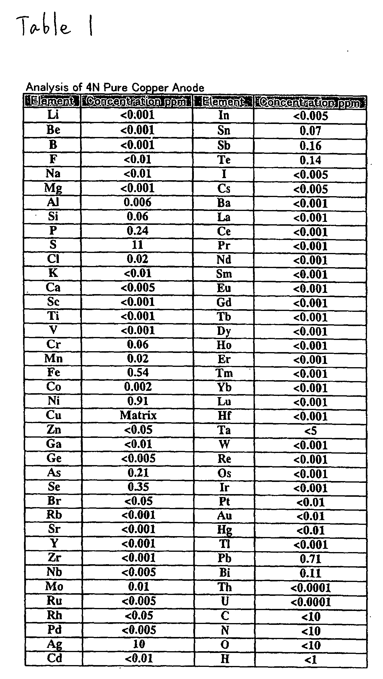
- Further, the oxygen content of each of the foregoing anodes was less than 10ppm. The analysis of the 4N pure copper anode is shown in Table 1.
- As the plating liquid, copper sulfate: 50g/L (Cu), sulfuric acid: 10g/L, chlorine ion 60mg/L, additive [brightening agent, surface active agent] (Product Name CC-1220: manufactured by Nikko Metal Plating): 1mL/L were used. The purity of the copper sulfate within the plating liquid was 99.99%.
- The plating conditions were plating temperature 30°C, cathode current density 4.0A/dm2, anode current density 4.0A/dm2, and plating time 12hr. The foregoing conditions and other conditions are shown in Table 2.
- After the plating, the generation of particles, plate appearance and embeddability were observed. The results are similarly shown in Table 2.
- Regarding the particle amount, after having performed electrolysis under the foregoing electrolytic conditions, the plating liquid was filtered with a filter of 0.2 µm, and the weight of the filtrate was measured thereby. Regarding the plate appearance, after having performed electrolysis under the foregoing electrolytic conditions, the object to be plated was exchanged, plating was conducted for 1 minute, and the existence of bums, clouding, swelling, abnormal deposition, foreign material adhesion and so on were observed visually. Regarding embeddability, the embeddability of the semiconductor wafer via having an aspect ratio of 5 (via diameter 0.2 µm) was observed in its cross section with an electronic microscope.
- As a result of the foregoing experiments, the amount of particles was 3030 to 3857mg in Examples 1 to 4, and the plate appearance and embeddability were favorable.

- As shown in Table 3, pure copper having a purity of 4N to 5N was used as the anode, and a semiconductor wafer was used as the cathode. The crystal grain size of these pure copper anodes was non-recrystallized and 2000 µm.
- As the plating liquid, copper sulfate: 50g/L (Cu), sulfuric acid: 10g/L, chlorine ion 60mg/L, additive [brightening agent, surface active agent] (Product Name CC-1220: manufactured by Nikko Metal Plating): 1mL/L were used. The purity of the copper sulfate within the plating liquid was 99.99%.
- The plating conditions were plating temperature 30°C, cathode current density 4.0A/dm2, anode current density 4.0A/dm2, and plating time 12hr.
- With the foregoing Examples 5 and 6, in particular, illustrated are examples in which the oxygen content was 4000ppm, respectively. The foregoing conditions and other conditions are shown in Table 3.
- After the plating, the generation of particles, plate appearance and embeddability were observed. The results are similarly shown in Table 3. Moreover, the observation of the amount of particles, plate appearance and embeddability was pursuant to the same method as with foregoing Examples 1 to 4.
- As a result of the foregoing experiments, the amount of particles was 125mg and 188mg in Examples 5 and 6, and the plate appearance and embeddability were favorable. In particular, although the foregoing Examples contained a prescribed amount of oxygen as described above, even in comparison to Examples 1 to 4, the reduction in the amount of particles can be acknowledged.
- Accordingly, it is evident that containing an adjusted amount of oxygen in the pure copper anode is effective in forming a stable plate coating without any particles.

- As shown in Table 3, pure copper having a crystal grain diameter of 30 µm was used as the anode, and a semiconductor wafer was used as the cathode. Regarding the purity of these copper anodes, pure copper of 4N and 5N of the same level as the Examples was used. Moreover, each of the anodes used has an oxygen content of less than 10ppm.
- As the plating liquid, copper sulfate: 50g/L (Cu), sulfuric acid: 10g/L, chlorine ion 60mg/L, additive [brightening agent, surface active agent] (Product Name CC-1220: manufactured by Nikko Metal Plating): 1mL/L were used. The purity of the copper sulfate within the plating liquid was 99.99%.
- The plating conditions were plating temperature 30°C, cathode current density 4.0A/dm2, anode current density 4.0A/dm2, and plating time 12hr. The foregoing conditions and other conditions are shown in Table 3.
- After the plating, the generation of particles, plate appearance and embeddability were observed. The results are similarly shown in Table 3.
- Moreover, the observation of the amount of particles, plate appearance and embeddability was pursuant to the same method as with the foregoing Examples. As a result of the foregoing experiments, the amount of particles in Comparative Examples 1 and 2 reached 6540 to 6955mg, and although the embeddability was favorable, the plate appearance was unfavorable.
- Accordingly, it has been confirmed that the crystal grain size of the pure copper anode significantly influences the generation of particles, and, by adding oxygen thereto, the generation of particles can be further suppressed.
- The present invention yields a superior effect in that upon performing electrolytic plating, it is capable of suppressing the generation of particles such as sludge produced on the anode side within the plating bath, and capable of significantly preventing the adhesion of particles to a semiconductor wafer.
Claims (14)
- An electrolytic copper plating method characterized in employing pure copper as the anode upon performing electrolytic copper plating, and performing electrolytic copper plating with said pure copper anode having a crystal grain diameter of 10 µm or less or 60 µm or more or a non-recrystallized anode.
- An electrolytic copper plating method characterized in employing pure copper as the anode upon performing electrolytic copper plating, and performing electrolytic copper plating with said pure copper anode having a crystal grain diameter of 5 µm or less or 100 µm or more or a non-recrystallized anode.
- An electrolytic copper plating method according to claim 1 or claim 2, characterized in using pure copper having a purity of 2N (99wt%) or higher, excluding gas components, as the anode.
- An electrolytic copper plating method according to claim 1 or claim 2, characterized in using pure copper having a purity of 3N (99.9wt%) to 6N (99.9999wt%), excluding gas components, as the anode.
- An electrolytic copper plating method according to each of claims 1 to 4, characterized in using pure copper having an oxygen content of 500 to 15000ppm as the anode.
- An electrolytic copper plating method according to each of claims 1 to 4, characterized in using pure copper having an oxygen content of 1000 to 10000ppm as the anode.
- A pure copper anode for performing electrolytic copper plating characterized in that said anode is used for performing electrolytic copper plating, pure copper is used as the anode, and the crystal grain diameter of said pure anode is 10 µm or less or 60 µm or more or non-recrystallized.
- A pure copper anode for performing electrolytic copper plating characterized in that said anode is used for performing electrolytic copper plating, pure copper is used as the anode, and the crystal grain diameter of said pure anode is 5 µm or less or 100 µm or more or non-recrystallized.
- A pure copper anode for electrolytic copper plating according to claim 7 or claim 8, characterized in having a purity of 2N (99wt%) or higher, excluding gas components.
- A pure copper anode for electrolytic copper plating according to claim 7 or claim 8, characterized in having a purity of 3N (99.9wt%) to 6N (99.9999wt%), excluding gas components.
- A pure copper anode for electrolytic copper plating according to each of claims 7 to 10, characterized in that said anode is used for performing electrolytic copper plating, and having an oxygen content of 500 to 15000ppm as the anode.
- A pure copper anode for electrolytic copper plating according to each of claims 7 to 10, characterized in that said anode is used for performing electrolytic copper plating, and having an oxygen content of 1000 to 10000ppm as the anode.
- An electrolytic copper plating method and a pure copper anode for electrolytic copper plating according to each of claims 1 to 12, characterized in that the electrolytic copper plating is to be performed on a semiconductor wafer.
- A semiconductor wafer having low particle adhesion plated with the electrolytic copper plating method and the pure copper anode for electrolytic copper plating according to each of claims 1 to 13.
Applications Claiming Priority (3)
| Application Number | Priority Date | Filing Date | Title |
|---|---|---|---|
| JP2001374212A JP4011336B2 (en) | 2001-12-07 | 2001-12-07 | Electro-copper plating method, pure copper anode for electro-copper plating, and semiconductor wafer plated with these with less particle adhesion |
| JP2001374212 | 2001-12-07 | ||
| PCT/JP2002/009014 WO2003048429A1 (en) | 2001-12-07 | 2002-09-05 | Copper electroplating method, pure copper anode for copper electroplating, and semiconductor wafer plated thereby with little particle adhesion |
Publications (2)
| Publication Number | Publication Date |
|---|---|
| EP1452628A1 true EP1452628A1 (en) | 2004-09-01 |
| EP1452628A4 EP1452628A4 (en) | 2007-12-05 |
Family
ID=19182806
Family Applications (1)
| Application Number | Title | Priority Date | Filing Date |
|---|---|---|---|
| EP02760809A Withdrawn EP1452628A4 (en) | 2001-12-07 | 2002-09-05 | COPPER ELECTRODEPOSITION PROCESS, PURE COPPER ANODE FOR COPPER ELECTRODEPOSITION, AND SEMICONDUCTOR WAFER COVERED BY THIS PROCESS HAVING LOW PARTICLE ADHESION |
Country Status (7)
| Country | Link |
|---|---|
| US (3) | US7648621B2 (en) |
| EP (1) | EP1452628A4 (en) |
| JP (1) | JP4011336B2 (en) |
| KR (1) | KR100603131B1 (en) |
| CN (1) | CN1273648C (en) |
| TW (1) | TWI260353B (en) |
| WO (1) | WO2003048429A1 (en) |
Cited By (1)
| Publication number | Priority date | Publication date | Assignee | Title |
|---|---|---|---|---|
| EP2213772A4 (en) * | 2007-11-01 | 2012-01-11 | Jx Nippon Mining & Metals Corp | COPPER OR COPPER ANODE CONTAINING PHOSPHORUS, PROCESS FOR ELECTROLYTIC COPPER DEPOSITION ON SEMICONDUCTOR WAFER, AND SEMICONDUCTOR WAFER WITHOUT SIGNIFICANT DEPOSITION OF PARTICLES THEREON |
Families Citing this family (19)
| Publication number | Priority date | Publication date | Assignee | Title |
|---|---|---|---|---|
| JP4011336B2 (en) * | 2001-12-07 | 2007-11-21 | 日鉱金属株式会社 | Electro-copper plating method, pure copper anode for electro-copper plating, and semiconductor wafer plated with these with less particle adhesion |
| JP4034095B2 (en) * | 2002-03-18 | 2008-01-16 | 日鉱金属株式会社 | Electro-copper plating method and phosphorous copper anode for electro-copper plating |
| US7887603B2 (en) * | 2002-09-05 | 2011-02-15 | Jx Nippon Mining & Metals Corporation | High purity copper sulfate and method for production thereof |
| US20060071338A1 (en) * | 2004-09-30 | 2006-04-06 | International Business Machines Corporation | Homogeneous Copper Interconnects for BEOL |
| KR100698063B1 (en) * | 2004-12-23 | 2007-03-23 | 동부일렉트로닉스 주식회사 | Electrochemical Plating Apparatus and Method |
| CN100576578C (en) * | 2006-04-20 | 2009-12-30 | 无锡尚德太阳能电力有限公司 | Method for preparing solar cell electrode and electrochemical deposition device thereof |
| JP5370979B2 (en) * | 2007-04-16 | 2013-12-18 | 国立大学法人茨城大学 | Manufacturing method of semiconductor integrated circuit |
| US20090250352A1 (en) * | 2008-04-04 | 2009-10-08 | Emat Technology, Llc | Methods for electroplating copper |
| JP5407273B2 (en) * | 2008-10-24 | 2014-02-05 | ソニー株式会社 | Negative electrode current collector, negative electrode and secondary battery |
| JP5376168B2 (en) * | 2010-03-30 | 2013-12-25 | 三菱マテリアル株式会社 | High purity copper anode for electrolytic copper plating, manufacturing method thereof, and electrolytic copper plating method |
| JP5590328B2 (en) * | 2011-01-14 | 2014-09-17 | 三菱マテリアル株式会社 | Phosphorus-containing copper anode for electrolytic copper plating and electrolytic copper plating method using the same |
| JP5626582B2 (en) * | 2011-01-21 | 2014-11-19 | 三菱マテリアル株式会社 | Phosphorus copper anode for electrolytic copper plating and electrolytic copper plating method using the same |
| JP6727749B2 (en) * | 2013-07-11 | 2020-07-22 | 三菱マテリアル株式会社 | Copper material for high purity copper sputtering target and high purity copper sputtering target |
| JP6619942B2 (en) * | 2015-03-06 | 2019-12-11 | Jx金属株式会社 | Copper anode or phosphorus-containing copper anode used for electrolytic copper plating on semiconductor wafer and method for producing copper anode or phosphorus-containing copper anode |
| CN104846422B (en) * | 2015-05-22 | 2017-04-26 | 深圳崇达多层线路板有限公司 | Electro-coppering device |
| CN107153084B (en) * | 2017-05-27 | 2020-05-22 | 佛山市承安铜业有限公司 | A method to study the influence of copper anode Cl- concentration on the quality of copper plating |
| CN107641821B (en) * | 2017-09-14 | 2019-06-07 | 上海新阳半导体材料股份有限公司 | A kind of copper sulfate baths, preparation method and application and electrolytic cell |
| CN112176372B (en) * | 2020-09-27 | 2021-10-15 | 东北大学 | A kind of method for preparing cobalt-tantalum alloy coating at low temperature by using cobalt dichloride and tantalum pentachloride as raw materials |
| CN113373404B (en) * | 2021-06-10 | 2022-09-27 | 中国科学院近代物理研究所 | Copper-based thick-wall Nb 3 Sn film superconducting cavity and preparation method thereof |
Family Cites Families (20)
| Publication number | Priority date | Publication date | Assignee | Title |
|---|---|---|---|---|
| US2923671A (en) * | 1957-03-19 | 1960-02-02 | American Metal Climax Inc | Copper electrodeposition process and anode for use in same |
| DE1916293B2 (en) * | 1969-03-29 | 1971-03-18 | PROCESS FOR PRODUCING A NIOB LAYER BY MELT FLOW ELECTROLYTIC DEPOSITION ON A COPPER CARRIER | |
| US4696729A (en) * | 1986-02-28 | 1987-09-29 | International Business Machines | Electroplating cell |
| JPH03116832A (en) * | 1989-09-29 | 1991-05-17 | Mitsubishi Electric Corp | Cleaning of solid surface |
| JP3403918B2 (en) * | 1997-06-02 | 2003-05-06 | 株式会社ジャパンエナジー | High purity copper sputtering target and thin film |
| US6372119B1 (en) * | 1997-06-26 | 2002-04-16 | Alcoa Inc. | Inert anode containing oxides of nickel iron and cobalt useful for the electrolytic production of metals |
| US6113771A (en) * | 1998-04-21 | 2000-09-05 | Applied Materials, Inc. | Electro deposition chemistry |
| JP4394234B2 (en) * | 2000-01-20 | 2010-01-06 | 日鉱金属株式会社 | Copper electroplating solution and copper electroplating method |
| JP2001240949A (en) * | 2000-02-29 | 2001-09-04 | Mitsubishi Materials Corp | Method for producing high-purity copper processed material having fine crystal grains |
| US6527920B1 (en) * | 2000-05-10 | 2003-03-04 | Novellus Systems, Inc. | Copper electroplating apparatus |
| US6821407B1 (en) * | 2000-05-10 | 2004-11-23 | Novellus Systems, Inc. | Anode and anode chamber for copper electroplating |
| TWI228548B (en) * | 2000-05-26 | 2005-03-01 | Ebara Corp | Apparatus for processing substrate and apparatus for processing treatment surface of substrate |
| US6531039B2 (en) * | 2001-02-21 | 2003-03-11 | Nikko Materials Usa, Inc. | Anode for plating a semiconductor wafer |
| JP4123330B2 (en) * | 2001-03-13 | 2008-07-23 | 三菱マテリアル株式会社 | Phosphorus copper anode for electroplating |
| JP4076751B2 (en) * | 2001-10-22 | 2008-04-16 | 日鉱金属株式会社 | Electro-copper plating method, phosphor-containing copper anode for electrolytic copper plating, and semiconductor wafer plated with these and having less particle adhesion |
| JP4011336B2 (en) * | 2001-12-07 | 2007-11-21 | 日鉱金属株式会社 | Electro-copper plating method, pure copper anode for electro-copper plating, and semiconductor wafer plated with these with less particle adhesion |
| US6830673B2 (en) * | 2002-01-04 | 2004-12-14 | Applied Materials, Inc. | Anode assembly and method of reducing sludge formation during electroplating |
| JP4034095B2 (en) * | 2002-03-18 | 2008-01-16 | 日鉱金属株式会社 | Electro-copper plating method and phosphorous copper anode for electro-copper plating |
| US20030188975A1 (en) * | 2002-04-05 | 2003-10-09 | Nielsen Thomas D. | Copper anode for semiconductor interconnects |
| JP5066577B2 (en) * | 2007-11-01 | 2012-11-07 | Jx日鉱日石金属株式会社 | Copper anode or phosphorus-containing copper anode, method of electrolytic copper plating on semiconductor wafer, and semiconductor wafer with less particle adhesion |
-
2001
- 2001-12-07 JP JP2001374212A patent/JP4011336B2/en not_active Expired - Lifetime
-
2002
- 2002-09-05 US US10/486,078 patent/US7648621B2/en not_active Expired - Lifetime
- 2002-09-05 CN CNB02817075XA patent/CN1273648C/en not_active Expired - Lifetime
- 2002-09-05 KR KR1020047008385A patent/KR100603131B1/en not_active Expired - Lifetime
- 2002-09-05 WO PCT/JP2002/009014 patent/WO2003048429A1/en not_active Ceased
- 2002-09-05 EP EP02760809A patent/EP1452628A4/en not_active Withdrawn
- 2002-11-18 TW TW091133588A patent/TWI260353B/en not_active IP Right Cessation
-
2009
- 2009-09-11 US US12/557,676 patent/US7799188B2/en not_active Expired - Lifetime
-
2010
- 2010-08-23 US US12/861,161 patent/US7943033B2/en not_active Expired - Fee Related
Non-Patent Citations (2)
| Title |
|---|
| No further relevant documents disclosed * |
| See also references of WO03048429A1 * |
Cited By (1)
| Publication number | Priority date | Publication date | Assignee | Title |
|---|---|---|---|---|
| EP2213772A4 (en) * | 2007-11-01 | 2012-01-11 | Jx Nippon Mining & Metals Corp | COPPER OR COPPER ANODE CONTAINING PHOSPHORUS, PROCESS FOR ELECTROLYTIC COPPER DEPOSITION ON SEMICONDUCTOR WAFER, AND SEMICONDUCTOR WAFER WITHOUT SIGNIFICANT DEPOSITION OF PARTICLES THEREON |
Also Published As
| Publication number | Publication date |
|---|---|
| US20040200727A1 (en) | 2004-10-14 |
| US20100000871A1 (en) | 2010-01-07 |
| KR100603131B1 (en) | 2006-07-20 |
| WO2003048429A1 (en) | 2003-06-12 |
| US7648621B2 (en) | 2010-01-19 |
| KR20050025298A (en) | 2005-03-14 |
| US7943033B2 (en) | 2011-05-17 |
| CN1273648C (en) | 2006-09-06 |
| TW200300804A (en) | 2003-06-16 |
| US20100307923A1 (en) | 2010-12-09 |
| JP4011336B2 (en) | 2007-11-21 |
| JP2003171797A (en) | 2003-06-20 |
| EP1452628A4 (en) | 2007-12-05 |
| CN1549876A (en) | 2004-11-24 |
| US7799188B2 (en) | 2010-09-21 |
| TWI260353B (en) | 2006-08-21 |
Similar Documents
| Publication | Publication Date | Title |
|---|---|---|
| US7943033B2 (en) | Electrolytic copper plating method, pure copper anode for electrolytic copper plating, and semiconductor wafer having low particle adhesion plated with said method and anode | |
| US8252157B2 (en) | Electrolytic copper plating method, phosphorous copper anode for electrolytic copper plating, and semiconductor wafer having low particle adhesion plated with said method and anode | |
| US7138040B2 (en) | Electrolytic copper plating method, phosphorous copper anode for electrolytic plating method, and semiconductor wafer having low particle adhesion plated with said method and anode | |
| EP2213772B1 (en) | Phosphorus-containing copper anode | |
| JP4064121B2 (en) | Electro-copper plating method using phosphorous copper anode | |
| JP4607165B2 (en) | Electro copper plating method | |
| JP4554662B2 (en) | Phosphorus copper anode for electrolytic copper plating and method for producing the same | |
| JP5234844B2 (en) | Electro-copper plating method, phosphor-containing copper anode for electrolytic copper plating, and semiconductor wafer plated with these and having less particle adhesion | |
| JP3916134B2 (en) | Anode for electrolytic copper plating, method for producing the anode, and electrolytic copper plating method using the anode | |
| WO2019187250A1 (en) | Co anode, and co electroplating method using co anode | |
| JP2011006794A (en) | Electrolytic copper plating method, phosphorous-containing copper anode for electrolytic copper plating, and semiconductor wafer with reduced sticking of particle plated using them |
Legal Events
| Date | Code | Title | Description |
|---|---|---|---|
| PUAI | Public reference made under article 153(3) epc to a published international application that has entered the european phase |
Free format text: ORIGINAL CODE: 0009012 |
|
| 17P | Request for examination filed |
Effective date: 20040116 |
|
| AK | Designated contracting states |
Kind code of ref document: A1 Designated state(s): AT BE BG CH CY CZ DE DK EE ES FI FR GB GR IE IT LI LU MC NL PT SE SK TR |
|
| RTI1 | Title (correction) |
Free format text: COPPER ELECTROPLATING METHOD, PURE COPPER ANODE FOR COPPER ELECTROPLATING AND SEMICONDUCTOR WAFER PLATED THEREBY WITH LIT |
|
| RAP1 | Party data changed (applicant data changed or rights of an application transferred) |
Owner name: NIKKO MATERIALS CO., LTD. |
|
| RAP1 | Party data changed (applicant data changed or rights of an application transferred) |
Owner name: NIPPON MINING & METALS CO., LTD. |
|
| A4 | Supplementary search report drawn up and despatched |
Effective date: 20071107 |
|
| RAP1 | Party data changed (applicant data changed or rights of an application transferred) |
Owner name: JX NIPPON MINING & METALS CORPORATION |
|
| 17Q | First examination report despatched |
Effective date: 20130923 |
|
| GRAP | Despatch of communication of intention to grant a patent |
Free format text: ORIGINAL CODE: EPIDOSNIGR1 |
|
| RIC1 | Information provided on ipc code assigned before grant |
Ipc: C25D 3/38 20060101AFI20160317BHEP Ipc: C25D 17/10 20060101ALI20160317BHEP Ipc: C25D 17/00 20060101ALI20160317BHEP Ipc: C25D 21/04 20060101ALI20160317BHEP Ipc: C25D 7/12 20060101ALI20160317BHEP |
|
| INTG | Intention to grant announced |
Effective date: 20160407 |
|
| RBV | Designated contracting states (corrected) |
Designated state(s): DE FR GB IT |
|
| STAA | Information on the status of an ep patent application or granted ep patent |
Free format text: STATUS: THE APPLICATION IS DEEMED TO BE WITHDRAWN |
|
| 18D | Application deemed to be withdrawn |
Effective date: 20160818 |