EP1452620A1 - Mask used for layer formation and process of making the mask - Google Patents
Mask used for layer formation and process of making the mask Download PDFInfo
- Publication number
- EP1452620A1 EP1452620A1 EP03028254A EP03028254A EP1452620A1 EP 1452620 A1 EP1452620 A1 EP 1452620A1 EP 03028254 A EP03028254 A EP 03028254A EP 03028254 A EP03028254 A EP 03028254A EP 1452620 A1 EP1452620 A1 EP 1452620A1
- Authority
- EP
- European Patent Office
- Prior art keywords
- linear elements
- linear
- mask assembly
- mask
- elements
- Prior art date
- Legal status (The legal status is an assumption and is not a legal conclusion. Google has not performed a legal analysis and makes no representation as to the accuracy of the status listed.)
- Granted
Links
- 238000000034 method Methods 0.000 title claims description 27
- 230000015572 biosynthetic process Effects 0.000 title description 5
- 230000000873 masking effect Effects 0.000 claims abstract description 26
- 239000000758 substrate Substances 0.000 claims description 16
- 239000000463 material Substances 0.000 claims description 14
- 238000004519 manufacturing process Methods 0.000 claims description 5
- 239000011347 resin Substances 0.000 claims description 4
- 229920005989 resin Polymers 0.000 claims description 4
- 239000002253 acid Substances 0.000 claims description 2
- 239000011248 coating agent Substances 0.000 claims 2
- 238000000576 coating method Methods 0.000 claims 2
- 239000010410 layer Substances 0.000 description 28
- 239000011247 coating layer Substances 0.000 description 10
- 238000007740 vapor deposition Methods 0.000 description 9
- 239000000853 adhesive Substances 0.000 description 5
- 230000001070 adhesive effect Effects 0.000 description 5
- 238000005323 electroforming Methods 0.000 description 4
- 238000005019 vapor deposition process Methods 0.000 description 4
- 238000010438 heat treatment Methods 0.000 description 2
- 238000007747 plating Methods 0.000 description 2
- 239000003795 chemical substances by application Substances 0.000 description 1
- 238000000151 deposition Methods 0.000 description 1
- 239000011888 foil Substances 0.000 description 1
- 239000002184 metal Substances 0.000 description 1
- 238000000206 photolithography Methods 0.000 description 1
- 229920002120 photoresistant polymer Polymers 0.000 description 1
- 238000004544 sputter deposition Methods 0.000 description 1
- 229910001220 stainless steel Inorganic materials 0.000 description 1
- 239000010935 stainless steel Substances 0.000 description 1
Images


Classifications
-
- G—PHYSICS
- G03—PHOTOGRAPHY; CINEMATOGRAPHY; ANALOGOUS TECHNIQUES USING WAVES OTHER THAN OPTICAL WAVES; ELECTROGRAPHY; HOLOGRAPHY
- G03F—PHOTOMECHANICAL PRODUCTION OF TEXTURED OR PATTERNED SURFACES, e.g. FOR PRINTING, FOR PROCESSING OF SEMICONDUCTOR DEVICES; MATERIALS THEREFOR; ORIGINALS THEREFOR; APPARATUS SPECIALLY ADAPTED THEREFOR
- G03F1/00—Originals for photomechanical production of textured or patterned surfaces, e.g., masks, photo-masks, reticles; Mask blanks or pellicles therefor; Containers specially adapted therefor; Preparation thereof
- G03F1/20—Masks or mask blanks for imaging by charged particle beam [CPB] radiation, e.g. by electron beam; Preparation thereof
-
- C—CHEMISTRY; METALLURGY
- C23—COATING METALLIC MATERIAL; COATING MATERIAL WITH METALLIC MATERIAL; CHEMICAL SURFACE TREATMENT; DIFFUSION TREATMENT OF METALLIC MATERIAL; COATING BY VACUUM EVAPORATION, BY SPUTTERING, BY ION IMPLANTATION OR BY CHEMICAL VAPOUR DEPOSITION, IN GENERAL; INHIBITING CORROSION OF METALLIC MATERIAL OR INCRUSTATION IN GENERAL
- C23C—COATING METALLIC MATERIAL; COATING MATERIAL WITH METALLIC MATERIAL; SURFACE TREATMENT OF METALLIC MATERIAL BY DIFFUSION INTO THE SURFACE, BY CHEMICAL CONVERSION OR SUBSTITUTION; COATING BY VACUUM EVAPORATION, BY SPUTTERING, BY ION IMPLANTATION OR BY CHEMICAL VAPOUR DEPOSITION, IN GENERAL
- C23C14/00—Coating by vacuum evaporation, by sputtering or by ion implantation of the coating forming material
- C23C14/04—Coating on selected surface areas, e.g. using masks
- C23C14/042—Coating on selected surface areas, e.g. using masks using masks
-
- G—PHYSICS
- G03—PHOTOGRAPHY; CINEMATOGRAPHY; ANALOGOUS TECHNIQUES USING WAVES OTHER THAN OPTICAL WAVES; ELECTROGRAPHY; HOLOGRAPHY
- G03F—PHOTOMECHANICAL PRODUCTION OF TEXTURED OR PATTERNED SURFACES, e.g. FOR PRINTING, FOR PROCESSING OF SEMICONDUCTOR DEVICES; MATERIALS THEREFOR; ORIGINALS THEREFOR; APPARATUS SPECIALLY ADAPTED THEREFOR
- G03F7/00—Photomechanical, e.g. photolithographic, production of textured or patterned surfaces, e.g. printing surfaces; Materials therefor, e.g. comprising photoresists; Apparatus specially adapted therefor
- G03F7/12—Production of screen printing forms or similar printing forms, e.g. stencils
Definitions
- the present invention relates to a mask used when forming a thin layer on a substrate, and a process of fabricating the mask.
- Vapor deposition, sputtering, CVD and similar processes are used to form thin layers from various kinds of material.
- the thin layers are shaped to a certain pattern or configuration, depending upon a purpose of use. If the vapor deposition process is performed with a mask having a fine opening pattern, the vapor deposition process can make a thin layer having a desired pattern.
- the mask is firmly attached to a substrate prior to vapor deposition.
- the material is then vapor-deposited on the substrate.
- the opening of the mask decides (controls) the area of vapor deposition so that a desired pattern of thin layer is made on the substrate.
- the mask is prepared by, for example, electroforming.
- a plating substrate with photoresist thereon is prepared, and a fine pattern of resist is made on the substrate by photolithography (i.e., the pattern making process) . As a result, some areas are covered with the resist and other areas are not on the substrate.
- a metal is electro-deposited over the no resist areas on the plating substrate (i.e., the electroforming process). After the electroforming, the deposited metallic layer is removed from the substrate (i.e. , the peeling or exfoliating process). The peeled metallic layer becomes the mask which has the opening of the same shape as the resist pattern.
- the mask has the opening that has a uniform width is prepared.
- This technique is disclosed in Japanese Patent Kokai No. 10-305670.
- the mask is thin so that the mask is easy to bend. Particularly, the mask bends as the mask becomes larger. If the mask bends during the layer forming process, the opening of the mask changes its shape so that the resulting layer does not have a desired pattern.
- an improved mask assembly having a predetermined opening pattern used to form a thin layer having the same pattern on a substrate.
- the mask assembly includes a frame having a window.
- the mask assembly also includes a masking part supported by an edge (periphery) of the window such that the masking part spans (bridges) the window of the frame.
- the masking part includes a plurality of shielding portions spaced from each other to form the predetermined opening pattern.
- Each shielding portion has at least one linear element.
- the shielding portion may have a plurality of parallel linear elements arranged next to each other.
- a method of making a mask assembly has a predetermined opening pattern used to form a thin layer of the same pattern on a substrate.
- the method includes providing a masking part that includes a plurality of linear elements arranged next to each other.
- the method also includes removing predetermined one or more linear elements to form the predetermined opening pattern. Since which linear element(s) should be removed can be determined arbitrarily, it is possible to make the opening having a desired pattern.
- a mask assembly 1 used for layer formation includes a rectangular frame 3 having a rectangular window 2.
- the frame 3 is a rigid plate member made from, for instance, SUS430 (stainless steel).
- the frame 3 supports a masking portion 4 on the edge of the window 2.
- the masking portion 4 is firmly attached to the frame 3 by means of adhesive or other connecting element (not shown).
- the masking portion 4 generally spans the window 2.
- the masking portion 4 includes a plurality of shielding (masking) parts 6.
- Each shielding part 6 includes a plurality of parallel linear elements 5 arranged next to each other.
- the linear element 5 is a resin wire having a 10-micrometer diameter. It should be noted that three linear elements 5 form a single shielding part 6 in Figure 1, but this is for the sake of easy illustration. In actuality, the shielding part 6 includes more linear elements 5. Ends of the linear elements 5 are located on the edge of the window 2 of the frame 3.
- the shielding parts 6 are spaced from each other.
- the shielding parts 6 and the window 2 in combination define a plurality of rectangular openings 7.
- the mask assembly 1 is used for vapor deposition (layer formation).
- the mask assembly 1 is placed such that the frame 3 faces a substrate across the masking portion 4.
- a vapor deposition material is supplied from the frame side and passes through the openings 7 to reach the substrate.
- the material then becomes a thin layer having a certain pattern, which is determined by the openings 7, on the substrate.
- Such vapor deposition process can make, for example, a bus line for organic electroluminescent elements and/or other parts.
- the linear elements 5 may be stacked in the thickness direction of the frame 3 or mask assembly 1 (i.e., the direction perpendicular to the drawing sheet of Figure 1) so that the masking part has a multi-layer structure.
- An example of a masking assembly having a multi-layer masking part is illustrated in Figure 2.
- the linear elements 5 (5U, 5L) of each shielding part 6A have a two-layer structure.
- the lower layer is indicated as the "first layer” and the upper layer is indicated as the "second layer.
- the linear elements 5L of the lower layer are directly placed on the frame 3, and the linear elements 5U of the upper layer are put on the lower linear elements 5L.
- each lower linear element 5L is located below the connecting line of two adjacent upper linear elements 5U.
- the masking assembly 1B includes a plurality of modified shielding parts 6B.
- Each shielding part 6B includes a coating layer 8 that covers the linear elements 5.
- the coating layer 8 seals a gap between each two adjacent linear elements 5.
- the vapor deposition material (unshaded arrow) do not pass the gaps of the linear elements 5.
- the resulting masking portion is designated at 4B.
- a suitable film may be employed. As shown in Figure 4, a film 9 may be attached over the linear elements 5 of each shielding part 6C. The resulting masking portion is designated at 4C, and the resulting masking assembly is designated at 1C.
- the parallel linear elements 5 are arranged close to each other and firmly attached to the frame 3 by an adhesive or other suitable connector. Arranging and attaching the linear elements 5 may be performed simultaneously or successively. Alternatively, arranging a certain number of linear elements 5, followed by the attaching process, may be repeated until the linear elements 5 close the entire window 2 of the frame 3.
- each opening 7 is determined by the number of the removed linear elements 5 and the diameter of each linear element. Accordingly, it is possible to arbitrarily determine the size (width) of each opening 7. It is also possible to arbitrarily determine the location of each opening 7.
- the processes of Figures 5B and 5C are repeated.
- the lower layer of linear elements 5L are laid on the frame 3, some of the lower linear elements 5L are removed, and then the upper layer of linear elements 5U are laid over the lower linear elements 5L, and some of the upper linear elements 5U are removed to form the openings 7.
- the coating layers 8 are formed over the remaining linear elements 5 as shown in Figure 6B. This is an example when the coating layers 8 are formed after the process of Figure 5C.
- the coating layer formation is performed before the process of Figure 5C (i.e. , if the coating layers 8 are formed over all the linear elements 5), the coating layers 8 applied onto the unnecessary linear elements 5 are removed together with the unnecessary linear elements 5 when the unnecessary linear elements 5 are removed.
- films 9 may be provided over the linear elements 5 to seal gaps of adjacent linear elements 5.
- the films 9 may be attached to the linear elements 5 by an adhesive. This will be described with reference to Figures 7A to 7D.
- the linear elements 5 are arranged side by side as shown in Figure 7A.
- the film 9 is applied to the linear elements 5 as shown in Figure 7B.
- the film 9 is, for example, a metallic foil, and is attached to the linear elements 5 by a suitable adhesive.
- the linear elements 5, together with the film 9, are firmly secured on the frame 3 as shown in Figure 7C.
- predetermined linear elements 5 are removed to form the openings 7 as shown in Figure 7D.
- the associated film is also removed.
- the mask 1C is prepared.
- All the linear elements 5 may not be made from a single material.
- the “to be removed” elements may be made from an acid-corrosive material and the “to remain” elements may be made from an acid-resistive material.
- the “to be removed” elements are those linear elements which are removed in the process of Figure 5C to form the openings 7.
- the frame 3 may also be made from the acid-resistive material. In this case, the process of Figure 5C to remove the unnecessary linear elements can be performed by immersing all the linear elements together with the frame 3 ( Figure 5B) in an acid pool (not shown).
- the linear elements 5 and frame 3 deform upon heating, the linear elements 5 may be fused and fixed to the frame 3 by heating. In this case, no fixing agent such as an adhesive is needed to connect the linear elements 5 onto the frame 3.
- the shape and location of the window 2 and the shape of the frame 3 are not limited to those illustrated and described.
- the window 2 may have any suitable polygonal shape.
Landscapes
- Chemical & Material Sciences (AREA)
- Chemical Kinetics & Catalysis (AREA)
- Engineering & Computer Science (AREA)
- Materials Engineering (AREA)
- Mechanical Engineering (AREA)
- Metallurgy (AREA)
- Organic Chemistry (AREA)
- Physics & Mathematics (AREA)
- General Physics & Mathematics (AREA)
- Physical Vapour Deposition (AREA)
- Electroluminescent Light Sources (AREA)
Abstract
Description
- The present invention relates to a mask used when forming a thin layer on a substrate, and a process of fabricating the mask.
- Vapor deposition, sputtering, CVD and similar processes are used to form thin layers from various kinds of material. The thin layers are shaped to a certain pattern or configuration, depending upon a purpose of use. If the vapor deposition process is performed with a mask having a fine opening pattern, the vapor deposition process can make a thin layer having a desired pattern.
- In this vapor deposition process, the mask is firmly attached to a substrate prior to vapor deposition. The material is then vapor-deposited on the substrate. The opening of the mask decides (controls) the area of vapor deposition so that a desired pattern of thin layer is made on the substrate. The mask is prepared by, for example, electroforming.
- The process of making the mask by electroforming will be described. First, a plating substrate with photoresist thereon is prepared, and a fine pattern of resist is made on the substrate by photolithography (i.e., the pattern making process) . As a result, some areas are covered with the resist and other areas are not on the substrate. Then, a metal is electro-deposited over the no resist areas on the plating substrate (i.e., the electroforming process). After the electroforming, the deposited metallic layer is removed from the substrate (i.e. , the peeling or exfoliating process). The peeled metallic layer becomes the mask which has the opening of the same shape as the resist pattern.
- In this manner, the mask has the opening that has a uniform width is prepared. This technique is disclosed in Japanese Patent Kokai No. 10-305670.
- The mask is thin so that the mask is easy to bend. Particularly, the mask bends as the mask becomes larger. If the mask bends during the layer forming process, the opening of the mask changes its shape so that the resulting layer does not have a desired pattern.
- According to one aspect of the present invention, there is provided an improved mask assembly having a predetermined opening pattern used to form a thin layer having the same pattern on a substrate. The mask assembly includes a frame having a window. The mask assembly also includes a masking part supported by an edge (periphery) of the window such that the masking part spans (bridges) the window of the frame. The masking part includes a plurality of shielding portions spaced from each other to form the predetermined opening pattern. Each shielding portion has at least one linear element. The shielding portion may have a plurality of parallel linear elements arranged next to each other.
- According to another aspect of the present invention, there is provided a method of making a mask assembly. The mask assembly has a predetermined opening pattern used to form a thin layer of the same pattern on a substrate. The method includes providing a masking part that includes a plurality of linear elements arranged next to each other. The method also includes removing predetermined one or more linear elements to form the predetermined opening pattern. Since which linear element(s) should be removed can be determined arbitrarily, it is possible to make the opening having a desired pattern.
- Other objects, aspects and advantages of the present invention will become apparent to those skilled in the art to which the present invention pertains from the subsequent detailed description of the invention and the appended claims, taken in conjunction with the accompanying drawings.
-
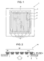
- Figure 1 illustrates a plan view of a mask assembly used for layer formation according to one embodiment of the present invention;
- Figure 2 illustrates a cross sectional view of a modified mask assembly according to the present invention;
- Figure 3 illustrates a cross sectional view of another modified mask assembly;
- Figure 4 illustrates a cross sectional view of still another modified mask assembly;
- Figures 5A to 5C are a set of plan views to illustrate a method of fabricating the mask assembly shown in Figure 1;
- Figures 6A and 6B are a set of cross sectional views to illustrate a method of fabricating the mask assembly shown in Figure 3; and
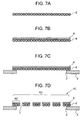
- Figures 7A to 7D are a set of cross sectional views to illustrate a method of fabricating the mask assembly shown in Figure 4.
-
- A mask assembly according to various embodiments of the present invention will be described with reference to the accompanying drawings.
- Referring to Figure 1, a
mask assembly 1 used for layer formation includes arectangular frame 3 having arectangular window 2. Theframe 3 is a rigid plate member made from, for instance, SUS430 (stainless steel). Theframe 3 supports amasking portion 4 on the edge of thewindow 2. Themasking portion 4 is firmly attached to theframe 3 by means of adhesive or other connecting element (not shown). Themasking portion 4 generally spans thewindow 2. - The
masking portion 4 includes a plurality of shielding (masking)parts 6. Eachshielding part 6 includes a plurality of parallellinear elements 5 arranged next to each other. Thelinear element 5 is a resin wire having a 10-micrometer diameter. It should be noted that threelinear elements 5 form asingle shielding part 6 in Figure 1, but this is for the sake of easy illustration. In actuality, theshielding part 6 includes morelinear elements 5. Ends of thelinear elements 5 are located on the edge of thewindow 2 of theframe 3. - The
shielding parts 6 are spaced from each other. Theshielding parts 6 and thewindow 2 in combination define a plurality ofrectangular openings 7. - The
mask assembly 1 is used for vapor deposition (layer formation). In a vapor deposition machine, themask assembly 1 is placed such that theframe 3 faces a substrate across themasking portion 4. A vapor deposition material is supplied from the frame side and passes through theopenings 7 to reach the substrate. The material then becomes a thin layer having a certain pattern, which is determined by theopenings 7, on the substrate. Such vapor deposition process can make, for example, a bus line for organic electroluminescent elements and/or other parts. - It should be noted that the
linear elements 5 may be stacked in the thickness direction of theframe 3 or mask assembly 1 (i.e., the direction perpendicular to the drawing sheet of Figure 1) so that the masking part has a multi-layer structure. An example of a masking assembly having a multi-layer masking part is illustrated in Figure 2. In Figure 2, the linear elements 5 (5U, 5L) of each shieldingpart 6A have a two-layer structure. The lower layer is indicated as the "first layer" and the upper layer is indicated as the "second layer. " Thelinear elements 5L of the lower layer are directly placed on theframe 3, and thelinear elements 5U of the upper layer are put on the lowerlinear elements 5L. In Figure 2, each lowerlinear element 5L is located below the connecting line of two adjacent upperlinear elements 5U. Since each lowerlinear element 5L seals a gap between the associated two upperlinear elements 5U, the vapor deposition material supplied, as indicated by the unshaded arrow, does not pass the gaps between the upperlinear elements 5U. The vapor deposition material flows through theopenings 7 only. Themulti-layer masking portion 4A includes a plurality ofmulti-layer shielding parts 6A to define the modifiedmasking assembly 1A. - Referring to Figure 3, another masking
assembly 1B is illustrated. The maskingassembly 1B includes a plurality of modifiedshielding parts 6B. Each shieldingpart 6B includes acoating layer 8 that covers thelinear elements 5. Thecoating layer 8 seals a gap between each two adjacentlinear elements 5. Thus, the vapor deposition material (unshaded arrow) do not pass the gaps of thelinear elements 5. The resulting masking portion is designated at 4B. - Instead of the
coating layer 8, a suitable film may be employed. As shown in Figure 4, a film 9 may be attached over thelinear elements 5 of each shieldingpart 6C. The resulting masking portion is designated at 4C, and the resulting masking assembly is designated at 1C. - Now, a process of making the mask assembly will be described.
- Firstly, referring to Figure 5A, the
frame 3 having thewindow 2 is prepared. Then, thelinear elements 5 are provided on theframe 3 to completely close thewindow 2 as indicated at 4' in Figure 5B. - The parallel
linear elements 5 are arranged close to each other and firmly attached to theframe 3 by an adhesive or other suitable connector. Arranging and attaching thelinear elements 5 may be performed simultaneously or successively. Alternatively, arranging a certain number oflinear elements 5, followed by the attaching process, may be repeated until thelinear elements 5 close theentire window 2 of theframe 3. - Tension is applied to the
linear elements 5 when thelinear elements 5 are attached to theframe 3. Therefore, the linear elements 5 (or the mask portion 4') which span thewindow 2 do not bend or become loose. - After the mask portion 4' is fixed to the
frame 3, at least onelinear element 5 is removed to form the opening (s) 7 as shown in Figure 5C. The width of eachopening 7 is determined by the number of the removedlinear elements 5 and the diameter of each linear element. Accordingly, it is possible to arbitrarily determine the size (width) of eachopening 7. It is also possible to arbitrarily determine the location of eachopening 7. - If the
linear elements 5 are stacked, the processes of Figures 5B and 5C are repeated. For example, when the mask shown in Figure 2 is fabricated, the lower layer oflinear elements 5L are laid on theframe 3, some of the lowerlinear elements 5L are removed, and then the upper layer oflinear elements 5U are laid over the lowerlinear elements 5L, and some of the upperlinear elements 5U are removed to form theopenings 7. - It should be noted that, as shown in Figure 3, coating layers 8 may be provided over the
linear elements 5 to seal gaps of adjacentlinear elements 5, before or after the process of Figure 5C. The coating layers 8 may be formed by vapor-depositing a resin on thelinear elements 5. This will be described with reference to Figures 6A and 6B. - When the predetermined linear elements are removed and the
openings 7 are formed as shown in Figure 6A, the coating layers 8 are formed over the remaininglinear elements 5 as shown in Figure 6B. This is an example when the coating layers 8 are formed after the process of Figure 5C. - Alternatively, if the coating layer formation is performed before the process of Figure 5C (i.e. , if the coating layers 8 are formed over all the linear elements 5), the coating layers 8 applied onto the unnecessary
linear elements 5 are removed together with the unnecessarylinear elements 5 when the unnecessarylinear elements 5 are removed. - It should also be noted that, as shown in Figure 4, films 9 may be provided over the
linear elements 5 to seal gaps of adjacentlinear elements 5. The films 9 may be attached to thelinear elements 5 by an adhesive. This will be described with reference to Figures 7A to 7D. - First, the
linear elements 5 are arranged side by side as shown in Figure 7A. Then, the film 9 is applied to thelinear elements 5 as shown in Figure 7B. The film 9 is, for example, a metallic foil, and is attached to thelinear elements 5 by a suitable adhesive. - Subsequently, the
linear elements 5, together with the film 9, are firmly secured on theframe 3 as shown in Figure 7C. Then, predeterminedlinear elements 5 are removed to form theopenings 7 as shown in Figure 7D. When the unnecessarylinear elements 5 are removed, the associated film is also removed. As a result, themask 1C is prepared. - It should be noted that the
linear element 5 is circle in the cross sectional shape in the foregoing description, but the present invention is not limited in this regard. For instance, thelinear element 5 may be polygonal in the cross sectional shape. - All the
linear elements 5 may not be made from a single material. For example, if thelinear elements 5 are categorized into "unnecessary" or "to be removed" elements and "necessary" or "to remain" elements, the "to be removed" elements may be made from an acid-corrosive material and the "to remain" elements may be made from an acid-resistive material. The "to be removed" elements are those linear elements which are removed in the process of Figure 5C to form theopenings 7. Theframe 3 may also be made from the acid-resistive material. In this case, the process of Figure 5C to remove the unnecessary linear elements can be performed by immersing all the linear elements together with the frame 3 (Figure 5B) in an acid pool (not shown). - If the
linear elements 5 andframe 3 deform upon heating, thelinear elements 5 may be fused and fixed to theframe 3 by heating. In this case, no fixing agent such as an adhesive is needed to connect thelinear elements 5 onto theframe 3. - The shape and location of the
window 2 and the shape of theframe 3 are not limited to those illustrated and described. For instance, thewindow 2 may have any suitable polygonal shape.
Claims (18)
- A mask assembly having a predetermined opening pattern used to form a thin layer having the same pattern on a substrate, comprising:a frame having a window, the window having an edge; anda masking part supported by the edge of the window, the masking part including a plurality of shielding portions spaced from each other to form the predetermined opening pattern, each shielding portion having at least one linear element.
- The mask assembly according to claim 1, wherein each of the plurality of shielding portions includes a plurality of parallel linear elements arranged next to each other.
- The mask assembly according to claim 2, wherein each of the plurality of shielding portions has a multi-layer structure made by the plurality of linear elements arranged in a plurality of layers.
- The mask assembly device according to claim 1, 2 or 3, wherein the predetermined opening pattern is made by removing predetermined one or more linear elements.
- The mask assembly according to any one of claims 1 to 4, wherein each of the plurality of shielding portions has a coating member to cover the at least one linear element.
- The mask assembly according to any one of claims 1 to 5, wherein each of the plurality of shielding portions has a film member to cover the at least one linear element.
- The mask assembly according to any one of claims 1 to 6, wherein each of the at least one linear element is made from an acid-resistive material.
- The mask assembly according to any one of claims 1 to 7, wherein each of the at least one linear element is a resin wire.
- The mask assembly according to any one of claims 3 to 8, wherein the multi-layer structure includes an upper layer and a lower layer, and the linear elements of the lower layer are arranged to seal gaps between the linear elements of the upper layer.
- A method of making a mask assembly, the mask assembly having a predetermined opening pattern used to form a thin layer of the same pattern on a substrate, comprising:providing a masking part that includes a plurality of linear elements; andremoving at least one predetermined linear element from the plurality of linear elements to form the predetermined opening pattern.
- The method according to claim 10, wherein the step of providing a masking part and the step of removing the at least one predetermined linear element are repeated at least twice.
- The method according to claim 10 or 11 further including providing a coating over the plurality of linear elements.
- The method according to claim 10, 11 or 12 further including providing a film over the plurality of linear elements.
- The method according to any one of claims 10 to 13, wherein the plurality of linear elements are made from an acid-resistive material except for the at least one predetermined linear element.
- The method according to any one of claims 10 to 14, wherein each of the plurality of linear elements is a resin wire.
- The method according to any one of claims 10 to 15, wherein the predetermined linear elements are made from an acid-corrosive material, and the step of removing the at least one predetermined linear element includes immersing the plurality of linear elements into an acid pool.
- The method according to any one of claims 10 to 16 further including attaching the plurality of linear elements on a frame.
- The method according to claim 17, wherein the step of attaching the plurality of linear elements is performed while a tension is being applied to the plurality of linear elements.
Applications Claiming Priority (2)
| Application Number | Priority Date | Filing Date | Title |
|---|---|---|---|
| JP2003015935 | 2003-01-24 | ||
| JP2003015935A JP2004225126A (en) | 2003-01-24 | 2003-01-24 | Film deposition mask, and method for manufacturing the same |
Publications (2)
| Publication Number | Publication Date |
|---|---|
| EP1452620A1 true EP1452620A1 (en) | 2004-09-01 |
| EP1452620B1 EP1452620B1 (en) | 2006-03-08 |
Family
ID=32732814
Family Applications (1)
| Application Number | Title | Priority Date | Filing Date |
|---|---|---|---|
| EP03028254A Expired - Lifetime EP1452620B1 (en) | 2003-01-24 | 2003-12-09 | Mask used for layer formation and process of making the mask |
Country Status (4)
| Country | Link |
|---|---|
| US (1) | US7189480B2 (en) |
| EP (1) | EP1452620B1 (en) |
| JP (1) | JP2004225126A (en) |
| DE (1) | DE60303861T2 (en) |
Families Citing this family (24)
| Publication number | Priority date | Publication date | Assignee | Title |
|---|---|---|---|---|
| US7115927B2 (en) * | 2003-02-24 | 2006-10-03 | Samsung Electronics Co., Ltd. | Phase changeable memory devices |
| CN101015234B (en) * | 2004-09-08 | 2010-10-13 | 东丽株式会社 | Organic electroluminescence device and manufacturing method thereof |
| WO2007011707A2 (en) | 2005-07-15 | 2007-01-25 | Micell Technologies, Inc. | Polymer coatings containing drug powder of controlled morphology |
| WO2007011708A2 (en) | 2005-07-15 | 2007-01-25 | Micell Technologies, Inc. | Stent with polymer coating containing amorphous rapamycin |
| KR101081180B1 (en) | 2005-12-13 | 2011-11-07 | 사천홍시현시기건유한공사 | Shadow mask and fabricating apparatus for the same |
| ES2540059T3 (en) | 2006-04-26 | 2015-07-08 | Micell Technologies, Inc. | Coatings containing multiple drugs |
| CA2667228C (en) | 2006-10-23 | 2015-07-14 | Micell Technologies, Inc. | Holder for electrically charging a substrate during coating |
| US11426494B2 (en) | 2007-01-08 | 2022-08-30 | MT Acquisition Holdings LLC | Stents having biodegradable layers |
| CA2679712C (en) | 2007-01-08 | 2016-11-15 | Micell Technologies, Inc. | Stents having biodegradable layers |
| CN102083397B (en) | 2008-04-17 | 2013-12-25 | 米歇尔技术公司 | Stents having bioabsorbable layers |
| JP2011528275A (en) | 2008-07-17 | 2011-11-17 | ミセル テクノロジーズ,インク. | Drug delivery medical device |
| KR101002185B1 (en) | 2008-11-12 | 2010-12-17 | 주식회사 야스 | Fixing wire mask and wire mask for manufacturing large area OLD |
| WO2010120552A2 (en) | 2009-04-01 | 2010-10-21 | Micell Technologies, Inc. | Coated stents |
| EP3366326A1 (en) | 2009-04-17 | 2018-08-29 | Micell Technologies, Inc. | Stents having controlled elution |
| EP2453834A4 (en) | 2009-07-16 | 2014-04-16 | Micell Technologies Inc | Drug delivery medical device |
| EP2531140B1 (en) | 2010-02-02 | 2017-11-01 | Micell Technologies, Inc. | Stent and stent delivery system with improved deliverability |
| KR101442941B1 (en) | 2010-03-09 | 2014-09-22 | 샤프 가부시키가이샤 | Vapor deposition mask, vapor deposition apparatus and vapor deposition method |
| EP2560576B1 (en) | 2010-04-22 | 2018-07-18 | Micell Technologies, Inc. | Stents and other devices having extracellular matrix coating |
| WO2012009684A2 (en) | 2010-07-16 | 2012-01-19 | Micell Technologies, Inc. | Drug delivery medical device |
| KR101759347B1 (en) * | 2010-12-14 | 2017-08-01 | 삼성디스플레이 주식회사 | Mask frame assembly for thin film deposition and the manufacturing method thereof |
| CA2841360A1 (en) | 2011-07-15 | 2013-01-24 | Micell Technologies, Inc. | Drug delivery medical device |
| US10188772B2 (en) | 2011-10-18 | 2019-01-29 | Micell Technologies, Inc. | Drug delivery medical device |
| KR20150143476A (en) | 2013-03-12 | 2015-12-23 | 미셀 테크놀로지즈, 인코포레이티드 | Bioabsorbable biomedical implants |
| HK1222313A1 (en) | 2013-05-15 | 2017-06-30 | Micell Technologies, Inc. | Bioabsorbable biomedical implants |
Citations (3)
| Publication number | Priority date | Publication date | Assignee | Title |
|---|---|---|---|---|
| US3241519A (en) * | 1962-04-05 | 1966-03-22 | Western Electric Co | Tensioned and cooled mask |
| EP0580112A1 (en) * | 1992-07-21 | 1994-01-26 | Matsushita Electric Industrial Co., Ltd. | Manufacturing method of glass optical elements having a fine concave and convex pattern and press-molding die therefor |
| JPH10315648A (en) * | 1997-05-22 | 1998-12-02 | Toppan Printing Co Ltd | Screen plate for screen printing and manufacturing method thereof |
Family Cites Families (3)
| Publication number | Priority date | Publication date | Assignee | Title |
|---|---|---|---|---|
| JP3786313B2 (en) | 1997-05-08 | 2006-06-14 | 九州日立マクセル株式会社 | Metal mask manufacturing method |
| KR100447990B1 (en) * | 1998-12-18 | 2004-11-08 | 주식회사 하이닉스반도체 | Stencil mask |
| US6855467B2 (en) * | 2000-09-05 | 2005-02-15 | Hoya Corporation | Transfer mask, method of dividing pattern or transfer mask, and method of manufacturing transfer mask |
-
2003
- 2003-01-24 JP JP2003015935A patent/JP2004225126A/en not_active Abandoned
- 2003-12-09 DE DE60303861T patent/DE60303861T2/en not_active Expired - Fee Related
- 2003-12-09 EP EP03028254A patent/EP1452620B1/en not_active Expired - Lifetime
-
2004
- 2004-01-05 US US10/750,975 patent/US7189480B2/en not_active Expired - Fee Related
Patent Citations (3)
| Publication number | Priority date | Publication date | Assignee | Title |
|---|---|---|---|---|
| US3241519A (en) * | 1962-04-05 | 1966-03-22 | Western Electric Co | Tensioned and cooled mask |
| EP0580112A1 (en) * | 1992-07-21 | 1994-01-26 | Matsushita Electric Industrial Co., Ltd. | Manufacturing method of glass optical elements having a fine concave and convex pattern and press-molding die therefor |
| JPH10315648A (en) * | 1997-05-22 | 1998-12-02 | Toppan Printing Co Ltd | Screen plate for screen printing and manufacturing method thereof |
Non-Patent Citations (1)
| Title |
|---|
| PATENT ABSTRACTS OF JAPAN vol. 1999, no. 03 31 March 1999 (1999-03-31) * |
Also Published As
| Publication number | Publication date |
|---|---|
| US20040144317A1 (en) | 2004-07-29 |
| EP1452620B1 (en) | 2006-03-08 |
| DE60303861D1 (en) | 2006-05-04 |
| DE60303861T2 (en) | 2006-11-16 |
| JP2004225126A (en) | 2004-08-12 |
| US7189480B2 (en) | 2007-03-13 |
Similar Documents
| Publication | Publication Date | Title |
|---|---|---|
| US7189480B2 (en) | Mask used for layer formation and process of making the mask | |
| US5846441A (en) | Method for forming a patterned metallic layer in a thin film magnetic head | |
| WO2006058081A2 (en) | Multiple shadow mask structure for deposition shadow mask protection and method of making and using same | |
| KR100561792B1 (en) | Method of manufacturing a plurality of electronic devices | |
| KR100704688B1 (en) | Manufacturing Method of Deposition Mask and Deposition Mask | |
| GB2025129A (en) | Lead tapes forsemiconductor devices | |
| KR102702151B1 (en) | Mask for vapor deposition | |
| EP0867929A3 (en) | Electronic interconnect structure and method for manufacturing it | |
| US4379737A (en) | Method to make a built up area rotary printing screen | |
| US4734617A (en) | Electroluminescent display and method of making same | |
| US6007729A (en) | Carrier tape and manufacturing method of said carrier tape | |
| US12044965B2 (en) | Method for forming components without adding tabs during etching | |
| US6379871B1 (en) | Method for fabricating a mask for a LIGA process | |
| US20130044041A1 (en) | Portable electronic device, antenna structure, and antenna producing process thereof | |
| WO2005013335A3 (en) | Method of depositing patterned films of materials using a positive imaging process | |
| JPS63303737A (en) | Metal mask for screen printing and its manufacture | |
| US4381966A (en) | Process for fabricating recording heads for magnetography | |
| JPS5997103A (en) | Manufacturing method of stepped relief type diffraction grating | |
| JPH04180231A (en) | Manufacture of semiconductor device provided with fine bump electrode | |
| TW202503920A (en) | Conductive material carrying mask and method for manufacturing conductive material carrying mask | |
| CN117568744A (en) | Mask manufacturing method | |
| EP1925192A1 (en) | Laminated substrate for mounting electronic parts | |
| US6238845B1 (en) | Method of forming lead frames with preformation support | |
| JP3878830B2 (en) | Manufacturing method of suspension for magnetic head | |
| JP2003014781A (en) | Probe substrate and method of manufacturing the same |
Legal Events
| Date | Code | Title | Description |
|---|---|---|---|
| PUAI | Public reference made under article 153(3) epc to a published international application that has entered the european phase |
Free format text: ORIGINAL CODE: 0009012 |
|
| AK | Designated contracting states |
Kind code of ref document: A1 Designated state(s): AT BE BG CH CY CZ DE DK EE ES FI FR GB GR HU IE IT LI LU MC NL PT RO SE SI SK TR |
|
| AX | Request for extension of the european patent |
Extension state: AL LT LV MK |
|
| 17P | Request for examination filed |
Effective date: 20040902 |
|
| RIN1 | Information on inventor provided before grant (corrected) |
Inventor name: HATA, TAKUYA,CORPORATE RES. & DEVELOPMENT LAB. Inventor name: SATOH, HIDEO,CORPORATE RES. & DEVELOPMENT LAB. Inventor name: UCHIDA, YOSHIHIKO,CORP. RES. & DEVELOPMENT LAB Inventor name: YOSHIZAWA, ATSUSHI,CORP. RES. & DEVELOPMENT LA Inventor name: CHUMAN, TAKASHI,CORPORATE RES. & DEVELOPMENT L |
|
| 17Q | First examination report despatched |
Effective date: 20041004 |
|
| GRAP | Despatch of communication of intention to grant a patent |
Free format text: ORIGINAL CODE: EPIDOSNIGR1 |
|
| AKX | Designation fees paid |
Designated state(s): DE FR GB |
|
| GRAS | Grant fee paid |
Free format text: ORIGINAL CODE: EPIDOSNIGR3 |
|
| RBV | Designated contracting states (corrected) |
Designated state(s): DE FR GB |
|
| GRAA | (expected) grant |
Free format text: ORIGINAL CODE: 0009210 |
|
| AK | Designated contracting states |
Kind code of ref document: B1 Designated state(s): DE FR GB |
|
| REG | Reference to a national code |
Ref country code: GB Ref legal event code: FG4D |
|
| REF | Corresponds to: |
Ref document number: 60303861 Country of ref document: DE Date of ref document: 20060504 Kind code of ref document: P |
|
| PLBE | No opposition filed within time limit |
Free format text: ORIGINAL CODE: 0009261 |
|
| STAA | Information on the status of an ep patent application or granted ep patent |
Free format text: STATUS: NO OPPOSITION FILED WITHIN TIME LIMIT |
|
| PGFP | Annual fee paid to national office [announced via postgrant information from national office to epo] |
Ref country code: DE Payment date: 20070208 Year of fee payment: 4 |
|
| 26N | No opposition filed |
Effective date: 20061211 |
|
| EN | Fr: translation not filed | ||
| PG25 | Lapsed in a contracting state [announced via postgrant information from national office to epo] |
Ref country code: FR Free format text: LAPSE BECAUSE OF FAILURE TO SUBMIT A TRANSLATION OF THE DESCRIPTION OR TO PAY THE FEE WITHIN THE PRESCRIBED TIME-LIMIT Effective date: 20070309 |
|
| GBPC | Gb: european patent ceased through non-payment of renewal fee |
Effective date: 20071209 |
|
| PG25 | Lapsed in a contracting state [announced via postgrant information from national office to epo] |
Ref country code: DE Free format text: LAPSE BECAUSE OF NON-PAYMENT OF DUE FEES Effective date: 20080701 |
|
| PG25 | Lapsed in a contracting state [announced via postgrant information from national office to epo] |
Ref country code: FR Free format text: LAPSE BECAUSE OF FAILURE TO SUBMIT A TRANSLATION OF THE DESCRIPTION OR TO PAY THE FEE WITHIN THE PRESCRIBED TIME-LIMIT Effective date: 20060308 |
|
| PG25 | Lapsed in a contracting state [announced via postgrant information from national office to epo] |
Ref country code: GB Free format text: LAPSE BECAUSE OF NON-PAYMENT OF DUE FEES Effective date: 20071209 |