EP1450388A2 - Plasma display panel - Google Patents
Plasma display panel Download PDFInfo
- Publication number
- EP1450388A2 EP1450388A2 EP04250343A EP04250343A EP1450388A2 EP 1450388 A2 EP1450388 A2 EP 1450388A2 EP 04250343 A EP04250343 A EP 04250343A EP 04250343 A EP04250343 A EP 04250343A EP 1450388 A2 EP1450388 A2 EP 1450388A2
- Authority
- EP
- European Patent Office
- Prior art keywords
- electrode portions
- electrode
- substrate
- portions
- discharge
- Prior art date
- Legal status (The legal status is an assumption and is not a legal conclusion. Google has not performed a legal analysis and makes no representation as to the accuracy of the status listed.)
- Withdrawn
Links
Images



Classifications
-
- H—ELECTRICITY
- H01—ELECTRIC ELEMENTS
- H01J—ELECTRIC DISCHARGE TUBES OR DISCHARGE LAMPS
- H01J11/00—Gas-filled discharge tubes with alternating current induction of the discharge, e.g. alternating current plasma display panels [AC-PDP]; Gas-filled discharge tubes without any main electrode inside the vessel; Gas-filled discharge tubes with at least one main electrode outside the vessel
- H01J11/10—AC-PDPs with at least one main electrode being out of contact with the plasma
- H01J11/12—AC-PDPs with at least one main electrode being out of contact with the plasma with main electrodes provided on both sides of the discharge space
-
- H—ELECTRICITY
- H01—ELECTRIC ELEMENTS
- H01J—ELECTRIC DISCHARGE TUBES OR DISCHARGE LAMPS
- H01J11/00—Gas-filled discharge tubes with alternating current induction of the discharge, e.g. alternating current plasma display panels [AC-PDP]; Gas-filled discharge tubes without any main electrode inside the vessel; Gas-filled discharge tubes with at least one main electrode outside the vessel
- H01J11/20—Constructional details
- H01J11/46—Connecting or feeding means, e.g. leading-in conductors
Definitions
- the present invention relates to a plasma display panel.
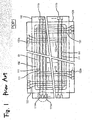
- Fig. 1 is a diagram showing an example of an electrode structure of a plasma display panel in the related art.
- a surface-discharge type dot matrix display-format plasma display panel (PDP1) includes a display-side glass substrate 110 and a back-side glass substrate 120, which are disposed facing each other with a predetermined gap therebetween.
- plural pairs of main discharge electrodes 111 which determines a main discharge cell for emitting light, are aligned as display electrodes so as to be parallel to each other in a horizontal (X) direction.
- Address electrodes 122 for selecting dots made to emit light are aligned in a vertical direction (Y) at an inner surface of the back-side glass substrate 120.
- the main discharge electrodes 111 and the address electrodes 122 are led, from inside a display region El enclosed by a sealing glass 132, to outer edge portions of the glass substrates 110 and 120. Particularly in the PDP1, in order to facilitate connection with drive circuits, one of the main discharge electrodes 111 of each pair and the other of the pair are sorted and led to the outer edge portions of both sides of the glass substrate 110.
- Terminal portions 111a, 111b, 122a and 122b, at which the main discharge electrodes 111 and the address electrodes 122 are expanded, are disposed at the outer edge portions of each of the glass substrates 110 and 120 in order to connect them to unillustrated drive circuits using a flexible cable or the like (Japanese Patent No.3084048(page 3 and Fig. 5)).
- One of the main discharge electrodes 111 of each pair (surface-discharge electrode pairs) described in the aforementioned prior art is a common electrode and the other of the pair is a scanning electrode.
- the terminals (111a in Fig. 1) of the outer edge portion of the plural common electrodes are independent terminals similar to the terminals (111b in Fig. 1) of the outer edge portion of the plural scanning electrodes.
- Eliminating the problem occurring in the aforementioned prior art can be given as one example of the problem that the invention attempts to solve, and it is an object of the invention to provide a plasma display panel that can improve the reliability of extraction terminal portions of common electrodes.
- a plasma display panel includes a pair of substrates, a plurality of surface-discharged electrode pairs, and a dielectric layer.
- the pair of substrates are disposed to face each other, with a discharge space sandwiched therebetween.
- the plurality of surface-discharge electrode pairs include scanning electrodes and common electrodes formed at an inner surface of one of the pair of substrates.
- the dielectric layer covers the surface-discharge electrode pairs with respect to the discharge space, wherein. Extraction electrode portions of the scanning electrodes are led to an end portion of one side of the one substrate.
- Extraction electrode portions of the common electrodes are led to an end portion of the other side of the one substrate.
- An island-shaped assembly electrode terminal portion that commonly connects the extraction electrode portions of the common electrodes is disposed. A plurality of micro openings are defined in the assembly electrode terminal portion.
- This embodiment is a surface-discharge type plasma display panel in which a display-side front substrate and a back-side back substrate are disposed facing each other with a discharge space sandwiched therebetween.
- the structure of surface-discharge electrode pairs thereof will be described in detail below with reference to Figs. 2 to 5.
- Fig. 2 is a diagram schematically showing an electrode structure of the plasma display panel of the embodiment of the invention.
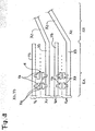
- Fig. 3 is a diagram showing the structure of surface-discharge electrode pairs (common electrodes and scanning electrodes) of Fig. 2.
- Fig. 4 is a diagram showing the cross-sectional structure of Fig. 2.
- Fig. 5 is an enlarged diagram of an A portion of Fig. 2.
- a display area EA of a plasma display panel in a display area EA of a plasma display panel 1, plural surface-discharge electrode pairs (common electrodes X1 to Xn and scanning electrodes Y1 to Yn) are aligned in parallel on a back surface of a front substrate 10, which is a display surface, so as to extend in a row direction (left and right directions in Fig. 2) of the front substrate 10.
- Bus electrode portions Xb which includes a metal film, of each common electrode Xi (i: 1 to n) are connected to narrow base end portions of transparent electrode portions Xa including a transparent conductive film such as ITO (Indium Tin Oxide) formed in a "T" shape.
- Bus electrode portions Yb of each scanning electrode Yi (i: 1 to n) are similarly connected to narrow base end portions of transparent electrode portions Ya including a transparent conductive film such as ITO formed in a "T" shape.
- the bus electrode portions Xb of the common electrodes Xi and the bus electrode portions Yb of the scanning electrodes Yi are alternatingly aligned in a column direction (up and down directions in Fig. 3) of the front substrate 10.
- the respective transparent electrode portions Xa and Ya which are juxtaposed along the bus electrode portions Xb and Yb, extend toward counterpart electrode sides so that top sides of wide portions of the transparent electrode portions Xa and Ya respectively face each other via a discharge gap g of a predetermined width.
- the common electrodes X1 to Xn and the scanning electrodes Y1 to Yn are configured so that extraction electrode portions Xc and Yc are led from inside the display area EA to non-display areas EB of outer edges of the front substrate 10, and the respective extraction electrode portions Xc and Yc of the common electrodes X1 to Xn and the scanning electrodes Y1 to Yn are respectively led to end portions of mutually different sides of the front substrate 10 (in Fig. 2, the extraction electrode portions Xc of the common electrodes X1 to Xn are led to a right-side end portion 12 and the extraction electrode portions Yc of the scanning electrodes Y1 to Yn are led to a left-side end portion 11).
- a dielectric layer 15 covers the surface-discharge electrode pairs (the common electrodes Xi and the scanning electrodes Yi) formed on the back surface of the front substrate 10.
- address electrodes D1 to Dm for selecting dots made to emit light are aligned in the vertical direction on an inner surface of a back substrate 20 disposed parallel to the front substrate 10.
- an address electrode Dj (j: 1 to m) is covered by a dielectric layer 21 and disposed facing the front substrate 10 with a discharge space 16 sandwiched therebetween.
- the extraction electrode portions Xc of the common electrodes X1 to Xn are commonly connected to an island-shaped assembly electrode terminal portion 13 at the right-side end portion 12, in which plural micro openings 14 are formed in a wide solid electrode.
- the extraction electrode portions Yc of the scanning electrodes Y1 to Yn are independent terminals and formed at the left-side end portion 11 so as to be connectable to external circuits.
- ITO is solidly vapor-deposited on the front substrate 10 and patterned by photolithography to form the transparent electrode portions Xa and Ya.
- a conductive sheet in which a conductive paste including metal power such as silver is made into a sheet, is transferred, patterned by photolithography and heated to simultaneously form the bus electrode portions Xb and Yb, the extraction electrode portions Xc and Yc and the island-shaped assembly electrode terminal portion 13 in which the plural micro openings 14 are formed.
- a dielectric film in which a glass paste including low-melting glass powder is made into a sheet, is transferred and heated to form the dielectric layer 15.
- the plasma display panel 1 of this embodiment includes the pair of substrates 10 and 20 disposed so as to face each other, with the discharge space 16 sandwiched therebetween; the plural surface-discharge electrode pairs including the scanning electrodes Yi (i: 1 to n) and the common electrodes Xi (i: 1 to n) formed at the inner surface of the front substrate 10 (one of the pair of substrates); and the dielectric layer 15 covering the surface-discharge electrode pairs with respect to the discharge space 16.
- the extraction electrode portions Yc of the scanning electrodes Yi are led to the end portion 11 of one side of the front substrate 10 and the extraction electrode portions Xc of the common electrodes Xi are led to the end portion 12 of the other side of the front substrate 10.
- the island-shaped assembly electrode terminal portion 13 that commonly connects the extraction electrode portions Xc of the common electrodes Xi is disposed.
- the plural micro openings 14 are disposed in the assembly electrode terminal portion 13 to form a mesh.
- the shape of the surface-discharge electrode pairs is not limited thereto and may be any shape as long as the present invention can be achieved.
Landscapes
- Physics & Mathematics (AREA)
- Engineering & Computer Science (AREA)
- Plasma & Fusion (AREA)
- Gas-Filled Discharge Tubes (AREA)
Abstract
Description
Claims (5)
- A plasma display panel comprising:a pair of substrates disposed to face each other, with a discharge space sandwiched therebetween;a plurality of surface-discharge electrode pairs including scanning electrodes and common electrodes formed at an inner surface of one of the pair of substrate; anda dielectric layer covering the surface-discharge electrode pairs with respect to the discharge space, wherein:extraction electrode portions of the scanning electrodes are led to an end portion of one side of the one substrate;extraction electrode portions of the common electrodes are led to an end portion of the other side of the one substrate,an island-shaped assembly electrode terminal portion that commonly connects the extraction electrode portions of the common electrodes is disposed; anda plurality of micro openings are defined in the assembly electrode terminal portion.
- The plasma display panel of claim 1, wherein:the scanning electrodes and the common electrodes each includes a transparent electrode portion and a bus electrode portion that includes a metal layer laminated on the transparent electrode portion; andthe extraction electrode portions and the assembly electrode terminal portion are formed by leading only the bus electrode portions to the end portion of the substrate.
- The plasma display panel of claim 1, wherein:the bus electrode portions, the extraction electrode portions and the assembly electrode terminal portion are formed by transferring and patterning , to the substrate, a conductive sheet in which a conductive paste including metal powder is made into a sheet, and patterning.
- The plasma display panel of claim 2, wherein:the bus electrode portions, the extraction electrode portions and the assembly electrode terminal portion are formed by transferring and patterning, to the substrate, a conductive sheet in which a conductive paste including metal powder is made into a sheet, and patterning.
- A method for manufacturing a surface-discharge electrode pair, the method comprising:depositing an transparent electrode material on a substrate:forming a pattern of transparent electrode portions on the transparent electrode material;transferring a conductive sheet onto the transparent electrode material; andforming patterns on the conductive sheet, bus electrode portions, extraction electrode portions and an assembly electrode terminal portion, wherein:the extraction electrode portions include two groups of electrode portions; andone of the two groups of electrode portions extend to one side of the substrate; andthe other of the two groups of electrode portions extend to the other side of the substrate.
Applications Claiming Priority (2)
| Application Number | Priority Date | Filing Date | Title |
|---|---|---|---|
| JP2003042002 | 2003-02-20 | ||
| JP2003042002A JP2004253231A (en) | 2003-02-20 | 2003-02-20 | Plasma display panel |
Publications (2)
| Publication Number | Publication Date |
|---|---|
| EP1450388A2 true EP1450388A2 (en) | 2004-08-25 |
| EP1450388A3 EP1450388A3 (en) | 2006-05-03 |
Family
ID=32732951
Family Applications (1)
| Application Number | Title | Priority Date | Filing Date |
|---|---|---|---|
| EP04250343A Withdrawn EP1450388A3 (en) | 2003-02-20 | 2004-01-22 | Plasma display panel |
Country Status (3)
| Country | Link |
|---|---|
| US (1) | US6998780B2 (en) |
| EP (1) | EP1450388A3 (en) |
| JP (1) | JP2004253231A (en) |
Cited By (1)
| Publication number | Priority date | Publication date | Assignee | Title |
|---|---|---|---|---|
| EP2051276A2 (en) * | 2005-04-06 | 2009-04-22 | Samsung SDI Co., Ltd. | Plasma display panel |
Families Citing this family (5)
| Publication number | Priority date | Publication date | Assignee | Title |
|---|---|---|---|---|
| SK2662004A3 (en) | 2002-11-20 | 2005-06-02 | Japan Tobacco, Inc. | 4-Oxoquinoline compound and its utilisation as integrase inhibitor |
| KR100626081B1 (en) * | 2005-05-19 | 2006-09-20 | 삼성에스디아이 주식회사 | Plasma Display Panel Driving Method |
| WO2007088623A1 (en) * | 2006-02-02 | 2007-08-09 | Shinoda Plasma Co., Ltd. | Display device |
| KR100852705B1 (en) * | 2006-09-15 | 2008-08-19 | 삼성에스디아이 주식회사 | Composition for forming electrode and plasma display panel manufactured therefrom |
| KR100778415B1 (en) | 2006-11-17 | 2007-11-22 | 삼성에스디아이 주식회사 | Plasma display panel |
Family Cites Families (6)
| Publication number | Priority date | Publication date | Assignee | Title |
|---|---|---|---|---|
| JP3084048B2 (en) | 1990-06-21 | 2000-09-04 | 富士通株式会社 | Plasma display panel |
| RU2089966C1 (en) * | 1995-11-22 | 1997-09-10 | Научно-производственная компания "Орион-Плазма" - Совместная акционерная компания закрытого типа | Ag gaseous-discharge display panel with reversing surface discharge |
| JPH11149874A (en) * | 1997-11-13 | 1999-06-02 | Pioneer Electron Corp | Plasma display panel |
| JP3626342B2 (en) * | 1997-12-19 | 2005-03-09 | パイオニア株式会社 | Surface discharge type plasma display panel |
| JP2000039865A (en) * | 1998-07-24 | 2000-02-08 | Matsushita Electric Ind Co Ltd | Plasma display device |
| US6118214A (en) * | 1999-05-12 | 2000-09-12 | Matsushita Electric Industrial Co., Ltd. | AC plasma display with apertured electrode patterns |
-
2003
- 2003-02-20 JP JP2003042002A patent/JP2004253231A/en active Pending
-
2004
- 2004-01-22 EP EP04250343A patent/EP1450388A3/en not_active Withdrawn
- 2004-02-20 US US10/781,909 patent/US6998780B2/en not_active Expired - Fee Related
Cited By (1)
| Publication number | Priority date | Publication date | Assignee | Title |
|---|---|---|---|---|
| EP2051276A2 (en) * | 2005-04-06 | 2009-04-22 | Samsung SDI Co., Ltd. | Plasma display panel |
Also Published As
| Publication number | Publication date |
|---|---|
| US20040217708A1 (en) | 2004-11-04 |
| JP2004253231A (en) | 2004-09-09 |
| EP1450388A3 (en) | 2006-05-03 |
| US6998780B2 (en) | 2006-02-14 |
Similar Documents
| Publication | Publication Date | Title |
|---|---|---|
| JP4287104B2 (en) | Organic EL display panel | |
| US6998780B2 (en) | Plasma display panel | |
| EP1589556A4 (en) | PLASMA SCREEN | |
| JPH06310040A (en) | Plasma display panel | |
| US7714508B2 (en) | Plasma display panel with enhanced bus electrode alignment | |
| US7459852B2 (en) | Plasma display panel having different structures on display and non-display areas | |
| US7375466B2 (en) | Address electrode design in a plasma display panel | |
| EP1536447B1 (en) | Plasma display panel and method of manufacturing the same | |
| KR100573139B1 (en) | Plasma Display Panel And Method Of Manufacturing The Same | |
| EP1748461A1 (en) | Plasma display panel and its driving method | |
| JP3560385B2 (en) | Plasma display panel and method of manufacturing the same | |
| CN1119782C (en) | plasma display device | |
| US7126278B2 (en) | Electrode structure, fabrication method thereof and PDP utilizing the same | |
| US20080024396A1 (en) | Front substrate of plasma display panel | |
| CN100407357C (en) | Electrode structure of front plate of plasma display and forming method thereof | |
| CN101770917B (en) | Plasma display panel | |
| CN1971827A (en) | Plasma display panel | |
| US7567035B2 (en) | Gas discharge display device and method for manufacturing the same | |
| KR100512797B1 (en) | A Plasma Display Panel | |
| US20060244381A1 (en) | Pdp having additional thin layers in the electrode pad | |
| CN101740292B (en) | Plasma display panel | |
| EP1672666A2 (en) | Plasma display panel | |
| US7573197B2 (en) | Plasma display panel with bus electrodes of the scan/sustain electrodes | |
| CN102376510B (en) | PDP (plasma display panel) discharge electrode and plasma display screen comprising same | |
| KR20010018861A (en) | Plasma display panel |
Legal Events
| Date | Code | Title | Description |
|---|---|---|---|
| PUAI | Public reference made under article 153(3) epc to a published international application that has entered the european phase |
Free format text: ORIGINAL CODE: 0009012 |
|
| AK | Designated contracting states |
Kind code of ref document: A2 Designated state(s): AT BE BG CH CY CZ DE DK EE ES FI FR GB GR HU IE IT LI LU MC NL PT RO SE SI SK TR |
|
| AX | Request for extension of the european patent |
Extension state: AL LT LV MK |
|
| 17P | Request for examination filed |
Effective date: 20050211 |
|
| PUAL | Search report despatched |
Free format text: ORIGINAL CODE: 0009013 |
|
| AK | Designated contracting states |
Kind code of ref document: A3 Designated state(s): AT BE BG CH CY CZ DE DK EE ES FI FR GB GR HU IE IT LI LU MC NL PT RO SE SI SK TR |
|
| AX | Request for extension of the european patent |
Extension state: AL LT LV MK |
|
| 17Q | First examination report despatched |
Effective date: 20061124 |
|
| AKX | Designation fees paid |
Designated state(s): DE FR GB |
|
| GRAP | Despatch of communication of intention to grant a patent |
Free format text: ORIGINAL CODE: EPIDOSNIGR1 |
|
| STAA | Information on the status of an ep patent application or granted ep patent |
Free format text: STATUS: THE APPLICATION IS DEEMED TO BE WITHDRAWN |
|
| 18D | Application deemed to be withdrawn |
Effective date: 20050209 |
|
| R18D | Application deemed to be withdrawn (corrected) |
Effective date: 20080209 |