EP1450386A1 - Switch control with light beams - Google Patents
Switch control with light beams Download PDFInfo
- Publication number
- EP1450386A1 EP1450386A1 EP03026271A EP03026271A EP1450386A1 EP 1450386 A1 EP1450386 A1 EP 1450386A1 EP 03026271 A EP03026271 A EP 03026271A EP 03026271 A EP03026271 A EP 03026271A EP 1450386 A1 EP1450386 A1 EP 1450386A1
- Authority
- EP
- European Patent Office
- Prior art keywords
- light beams
- mems
- switches
- generating
- light
- Prior art date
- Legal status (The legal status is an assumption and is not a legal conclusion. Google has not performed a legal analysis and makes no representation as to the accuracy of the status listed.)
- Granted
Links
Images


Classifications
-
- H—ELECTRICITY
- H01—ELECTRIC ELEMENTS
- H01H—ELECTRIC SWITCHES; RELAYS; SELECTORS; EMERGENCY PROTECTIVE DEVICES
- H01H61/00—Electrothermal relays
- H01H61/01—Details
- H01H61/013—Heating arrangements for operating relays
-
- H—ELECTRICITY
- H01—ELECTRIC ELEMENTS
- H01H—ELECTRIC SWITCHES; RELAYS; SELECTORS; EMERGENCY PROTECTIVE DEVICES
- H01H1/00—Contacts
- H01H1/0036—Switches making use of microelectromechanical systems [MEMS]
-
- H—ELECTRICITY
- H01—ELECTRIC ELEMENTS
- H01H—ELECTRIC SWITCHES; RELAYS; SELECTORS; EMERGENCY PROTECTIVE DEVICES
- H01H61/00—Electrothermal relays
Definitions
- the present invention relates generally to control of switches, and more specifically, relates to control of switches with light beams.
- Micro electromechanical switches are finding applications in a variety of fields.
- the MEMs typically are controlled by control lines etched onto semiconductor chips.
- the control lines occupy a significant percentage of the available chip real estate.
- the large number of requisite control lines quickly overwhelm the available area on the chip, thereby limiting performance.
- the preferred embodiment is useful in an array of micro electromechanical switches.
- the preferred embodiment comprises generating one or more light beams.
- the one or more light beams are directed onto predetermined ones of the switches, preferably with a positioning unit which may comprise, for example, a laser and mirror or an array of light emitting diodes.
- switches may be controlled with hardware which is smaller and lighter than the known hardware.
- thousands of switches may be activated and controlled quickly without any wiring system.
- Figure 1 is a schematic diagram illustrating a conventional prior art circuit board for a 15 element MEMs circuit accessed by control wires which are grown into the circuit board.
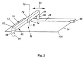
- Figure 2 is a schematic diagram illustrating a preferred embodiment of the invention utilizing a laser beam and mirror.
- Figure 3 is a schematic diagram illustrating an alternative embodiment of the invention utilizing a row of light emitting diodes mounted on a movable scan bar.
- a conventional MEMs circuit comprises a circuit board 10 on which 15 MEMs 21-35 (represented by dots) are mounted in a well known manner.
- MEMs 21-25 are arranged in a row along a line 40
- MEMs 26-30 are arranged in a row along a line 41
- MEMs 31-35 are arranged in a row along a line 42.
- the MEMs 21-35 are spaced 1 unit from each other and are accessed and controlled by independent conductors grown into circuit board 10, such as control lines 51, 52 and 53.
- Circuit board 10 may comprise a semiconductor chip, or a conventional circuit board on which copper control lines are etched. Additional details about MEMs and lines used to control them are described in U.S. application no. 09/676,007, entitled “Radio Receiver Automatic Frequency Control Techniques," filed September 29, 2000, in the name of Michael H. Myers, assigned to a common assignee and incorporated into this application by reference.
- circuit board 10 is a micro-thruster for an orbiting satellite.
- a small resistor connected to the control line (not shown) is heated which causes the actuation of MEMs 25, connected to the energized control line.
- the actuated MEMs creates a micro-thrust.
- the preferred embodiment includes a circuit board 10A which is like board 10, except that there is no need for control lines 50.
- a source of light such as a laser 60, is located at one end of board 10A as shown.
- the term light means not only visible light, but other radiation in the electromagnetic spectrum near the visible light band, including infrared radiation and ultraviolet radiation.
- Laser 60 generates a laser beam along a path 62 to a positioning unit 70 which includes a mirror 72 having a flat reflective surface 74.
- Surface 74 reflects the laser beam onto MEMs 32 along a path 63, thereby actuating MEMs 32.
- Mirror 72 is rotatable around a vertical axis 76 in order to move path 63 to other MEMs aligned with MEMs 32, such as MEMs 27 and 22.
- Positioning unit 70 also includes a scanning unit 80 which comprises a bar 82 arranged parallel to the surface of board 10A.
- Mirror 72 is rotatably mounted on bar 82 as shown.
- Bar 82 is carried by legs 84 and 86 which in turn are carried by wheels 88 and 90.
- the wheels 88 and 90 are rotated to cause bar 82 to move in the opposite directions indicated by arrow 92.
- bar 82 can be moved from end 12 to end 14 of board 10A and from end 14 to end 12.
- laser 60 is pulsed to generate pulses of light along path 62.
- Mirror 72 reflects the pulses of light onto desired MEMs. Scanning is performed one row at a time while bar 82 is moved in one of the directions indicated by arrow 92, and rotating mirror 72 is moved to cover each MEMs on board 10A.
- a pulse of light from laser 60 has enough energy to actuate one of the MEMs in a well known manner.
- an optical window could be used to seal the MEMs, and laser light of sufficient intensity could be directed through the window to actuate the MEMs.
- a resistive element could be buried just below the surface of the MEMs, and the light beam could be directed against the resistor.
- mirror 72 could be angled to cover the MEMs on board 10A in sectors.
- bar 82 could remain stationary.
- the underside of bar 82 is fitted with three light emitting diodes 101-103 aligned in a row corresponding to a column of MEMs, such as 23, 28 and 33. That is, diodes 101-103 are spaced in the same manner as a column of MEMs, such as 23, 28 and 33.
- bar 82 is moved from end 12 to end 14 of board 10A so that diodes 101-13 pass over successive columns of MEMs.
- the diodes are selectively pulsed to generate one to three beams of light which strike selected ones of the MEMs.
- the beams of light from the diodes actuate the MEMs in the same manner described in connection with the laser beam shown in Figure 2.
Landscapes
- Physics & Mathematics (AREA)
- Electromagnetism (AREA)
- Mechanical Light Control Or Optical Switches (AREA)
Abstract
Description
- The present invention relates generally to control of switches, and more specifically, relates to control of switches with light beams.
- Micro electromechanical switches (MEMs) are finding applications in a variety of fields. The MEMs typically are controlled by control lines etched onto semiconductor chips. For many applications, the control lines occupy a significant percentage of the available chip real estate. For example, in applications involving thousands of MEMs, the large number of requisite control lines quickly overwhelm the available area on the chip, thereby limiting performance. This invention addresses the problem and provides a solution.
- The preferred embodiment is useful in an array of micro electromechanical switches. In such an environment, the preferred embodiment comprises generating one or more light beams. The one or more light beams are directed onto predetermined ones of the switches, preferably with a positioning unit which may comprise, for example, a laser and mirror or an array of light emitting diodes.
- By using the foregoing techniques, switches may be controlled with hardware which is smaller and lighter than the known hardware. In addition, thousands of switches may be activated and controlled quickly without any wiring system.
- Figure 1 is a schematic diagram illustrating a conventional prior art circuit board for a 15 element MEMs circuit accessed by control wires which are grown into the circuit board.
- Figure 2 is a schematic diagram illustrating a preferred embodiment of the invention utilizing a laser beam and mirror.
- Figure 3 is a schematic diagram illustrating an alternative embodiment of the invention utilizing a row of light emitting diodes mounted on a movable scan bar.
- Referring to Figure 1, a conventional MEMs circuit comprises a
circuit board 10 on which 15 MEMs 21-35 (represented by dots) are mounted in a well known manner. MEMs 21-25 are arranged in a row along aline 40, MEMs 26-30 are arranged in a row along aline 41, and MEMs 31-35 are arranged in a row along aline 42. The MEMs 21-35 are spaced 1 unit from each other and are accessed and controlled by independent conductors grown intocircuit board 10, such ascontrol lines Circuit board 10 may comprise a semiconductor chip, or a conventional circuit board on which copper control lines are etched. Additional details about MEMs and lines used to control them are described in U.S. application no. 09/676,007, entitled "Radio Receiver Automatic Frequency Control Techniques," filed September 29, 2000, in the name of Michael H. Myers, assigned to a common assignee and incorporated into this application by reference. - One application for
circuit board 10 is a micro-thruster for an orbiting satellite. When current is applied to one ofcontrol line 51, a small resistor connected to the control line (not shown) is heated which causes the actuation ofMEMs 25, connected to the energized control line. The actuated MEMs creates a micro-thrust. - Referring to Figure 2, the preferred embodiment includes a
circuit board 10A which is likeboard 10, except that there is no need for control lines 50. A source of light, such as alaser 60, is located at one end ofboard 10A as shown. As used in this specification, the term light means not only visible light, but other radiation in the electromagnetic spectrum near the visible light band, including infrared radiation and ultraviolet radiation. -
Laser 60 generates a laser beam along apath 62 to apositioning unit 70 which includes amirror 72 having a flatreflective surface 74.Surface 74 reflects the laser beam ontoMEMs 32 along apath 63, thereby actuatingMEMs 32. Mirror 72 is rotatable around avertical axis 76 in order to movepath 63 to other MEMs aligned withMEMs 32, such asMEMs -
Positioning unit 70 also includes ascanning unit 80 which comprises abar 82 arranged parallel to the surface ofboard 10A.Mirror 72 is rotatably mounted onbar 82 as shown.Bar 82 is carried bylegs wheels wheels bar 82 to move in the opposite directions indicated byarrow 92. Thus,bar 82 can be moved fromend 12 toend 14 ofboard 10A and fromend 14 toend 12. - In use,
laser 60 is pulsed to generate pulses of light alongpath 62.Mirror 72 reflects the pulses of light onto desired MEMs. Scanning is performed one row at a time whilebar 82 is moved in one of the directions indicated byarrow 92, and rotatingmirror 72 is moved to cover each MEMs onboard 10A. A pulse of light fromlaser 60 has enough energy to actuate one of the MEMs in a well known manner. For example, an optical window could be used to seal the MEMs, and laser light of sufficient intensity could be directed through the window to actuate the MEMs. Alternatively, a resistive element could be buried just below the surface of the MEMs, and the light beam could be directed against the resistor. The light striking the resistor would heat the resistor which, in turn, would heat the MEMs to cause actuation. If a MEMs is not intended to be actuated,laser 60 is momentarily deactivated so that no light is generated aspath 63 is positioned toward the MEMs. - As an alternatively to the embodiment shown in Figure 2,
mirror 72 could be angled to cover the MEMs onboard 10A in sectors. In this embodiment,bar 82 could remain stationary. - Referring to Figure 3, the underside of
bar 82 is fitted with three light emitting diodes 101-103 aligned in a row corresponding to a column of MEMs, such as 23, 28 and 33. That is, diodes 101-103 are spaced in the same manner as a column of MEMs, such as 23, 28 and 33. In use,bar 82 is moved fromend 12 toend 14 ofboard 10A so that diodes 101-13 pass over successive columns of MEMs. Asbar 82 passes over the MEMs, the diodes are selectively pulsed to generate one to three beams of light which strike selected ones of the MEMs. The beams of light from the diodes actuate the MEMs in the same manner described in connection with the laser beam shown in Figure 2. - While particular elements, embodiments and applications of the present invention have been shown and described, it will be understood that the invention is not limited thereto since modifications may be made by those skilled in the art, particularly in light of the foregoing teachings. It is therefore contemplated by the appended claims to cover such modifications as incorporate those features which come within the spirit and scope of the invention. For example, thousand or tens of thousands of switches may be activated and controlled by this system. Or as another example, the light beams described in the specification need not be used to activate only micro thruster MEMs, but could be used to activate other types of MEMs, such as phase shifters for phased arrays. In the latter case, the MEMs would be configured for multiple activation and reset and not just for single firings. The intensity of the light in the beams could be used to shift the phase and/or amplitude of a phase shifter circuit.
Claims (16)
- In an array of micro electromechanical switches, apparatus for actuating the switches comprising:a source of a light beams; anda positioning unit arranged to direct the light beams onto a predetermined ones of said switches.
- Apparatus, as claimed in claim 1, wherein said light beam comprises a beam of infrared radiation.
- Apparatus, as claimed in claim 1, wherein said light beam comprises a beam of ultraviolet radiation.
- Apparatus, as claimed in claim 1, wherein said source comprises a laser.
- Apparatus, as claimed in claim 4, wherein said positioning unit comprises a rotatable mirror.
- Apparatus, as claimed in claim 5, wherein said positioning unit further comprises a scanning unit carrying said mirror, said scanning unit being movable with respect to said array of micro electromechanical switches.
- Apparatus, as claimed in claim 1, wherein said source comprises a plurality of light emitting diodes.
- Apparatus, as claimed in claim 7, wherein said positioning unit comprises a scanning unit carrying said plurality of light emitting diodes, said scanning unit being movable with respect to said array of micro electromechanical switches.
- In an array of micro electromechanical switches, a method of actuating the switches comprising:generating a plurality of light beams; anddirecting each of said light beams onto a predetermined one of said switches.
- A method, as claimed in claim 9, wherein said generating said plurality of light beams comprises generating infrared radiation.
- A method, as claimed in claim 9, wherein said generating said plurality of light beams comprises generating ultraviolet radiation.
- A method, as claimed in claim 9, wherein said generating said plurality of light beams comprises generating one or more laser beams.
- A method, as claimed in claim 12, wherein said directing comprises reflecting.
- A method, as claimed in claim 13, wherein said reflecting is accomplished with a reflecting surface and wherein said reflecting further comprises moving said reflecting surface with respect to said array of micro electromechanical switches.
- A method, as claimed in claim 9, wherein said generating comprises generating a plurality of said light beams arranged in a row.
- A method, as claimed in claim 15, wherein said directing comprises moving said light beams with respect to said array of micro electromechanical switches.
Applications Claiming Priority (2)
| Application Number | Priority Date | Filing Date | Title |
|---|---|---|---|
| US371365 | 1989-06-26 | ||
| US10/371,365 US6975783B2 (en) | 2003-02-19 | 2003-02-19 | Switch control with light beams |
Publications (2)
| Publication Number | Publication Date |
|---|---|
| EP1450386A1 true EP1450386A1 (en) | 2004-08-25 |
| EP1450386B1 EP1450386B1 (en) | 2006-02-08 |
Family
ID=32736455
Family Applications (1)
| Application Number | Title | Priority Date | Filing Date |
|---|---|---|---|
| EP03026271A Expired - Lifetime EP1450386B1 (en) | 2003-02-19 | 2003-11-14 | Switch control with light beams |
Country Status (3)
| Country | Link |
|---|---|
| US (1) | US6975783B2 (en) |
| EP (1) | EP1450386B1 (en) |
| DE (1) | DE60303477T2 (en) |
Cited By (1)
| Publication number | Priority date | Publication date | Assignee | Title |
|---|---|---|---|---|
| WO2007031468A1 (en) * | 2005-09-13 | 2007-03-22 | Siemens Aktiengesellschaft | Method for operation of an electrical switching device, and an electrical switching device operated using this method |
Citations (4)
| Publication number | Priority date | Publication date | Assignee | Title |
|---|---|---|---|---|
| US5955817A (en) * | 1996-12-16 | 1999-09-21 | Mcnc | Thermal arched beam microelectromechanical switching array |
| US20020080834A1 (en) * | 1999-04-07 | 2002-06-27 | Lasertec Corporation | Light source device |
| US6417807B1 (en) * | 2001-04-27 | 2002-07-09 | Hrl Laboratories, Llc | Optically controlled RF MEMS switch array for reconfigurable broadband reflective antennas |
| US20030012487A1 (en) * | 2001-01-29 | 2003-01-16 | Hamerly Mike E. | Optical switch based on rotating vertical micro-mirror |
Family Cites Families (15)
| Publication number | Priority date | Publication date | Assignee | Title |
|---|---|---|---|---|
| US12487A (en) * | 1855-03-06 | Osiill eor geinding a boltingr sumac | ||
| US80834A (en) * | 1868-08-11 | Improvement in clasp foe boots and shoes, belts foe ladies dresses | ||
| US4303302A (en) * | 1979-10-30 | 1981-12-01 | Gte Laboratories Incorporated | Piezoelectric optical switch |
| US5544268A (en) * | 1994-09-09 | 1996-08-06 | Deacon Research | Display panel with electrically-controlled waveguide-routing |
| US6075239A (en) * | 1997-09-10 | 2000-06-13 | Lucent Technologies, Inc. | Article comprising a light-actuated micromechanical photonic switch |
| JPH11149050A (en) * | 1997-11-15 | 1999-06-02 | Canon Inc | Optical deflection device |
| GB9828469D0 (en) * | 1998-12-24 | 1999-02-17 | British Aerospace | A modulated fibre bragg grating strain gauge assembly for absolute gauging of strain |
| US6310339B1 (en) * | 1999-10-28 | 2001-10-30 | Hrl Laboratories, Llc | Optically controlled MEM switches |
| US6453084B1 (en) * | 2000-01-17 | 2002-09-17 | Optical Switch Corporation | System and method for beam-steering using a reference signal feedback |
| US6253001B1 (en) * | 2000-01-20 | 2001-06-26 | Agilent Technologies, Inc. | Optical switches using dual axis micromirrors |
| US6785038B2 (en) * | 2001-01-17 | 2004-08-31 | Optical Coating Laboratory, Inc. | Optical cross-connect with magnetic micro-electro-mechanical actuator cells |
| US6763160B2 (en) * | 2001-04-26 | 2004-07-13 | Creo Srl | Optical cross connect switch having improved alignment control system |
| US6743988B2 (en) * | 2001-05-23 | 2004-06-01 | Lucent Technologies Inc. | Optically controlled switches |
| US6738539B2 (en) * | 2001-10-03 | 2004-05-18 | Continuum Photonics | Beam-steering optical switching apparatus |
| US6836589B2 (en) * | 2002-03-27 | 2004-12-28 | Nortel Networks, Ltd. | Low loss optical switch using dual axis piezo actuation and sensing |
-
2003
- 2003-02-19 US US10/371,365 patent/US6975783B2/en not_active Expired - Lifetime
- 2003-11-14 EP EP03026271A patent/EP1450386B1/en not_active Expired - Lifetime
- 2003-11-14 DE DE60303477T patent/DE60303477T2/en not_active Expired - Fee Related
Patent Citations (4)
| Publication number | Priority date | Publication date | Assignee | Title |
|---|---|---|---|---|
| US5955817A (en) * | 1996-12-16 | 1999-09-21 | Mcnc | Thermal arched beam microelectromechanical switching array |
| US20020080834A1 (en) * | 1999-04-07 | 2002-06-27 | Lasertec Corporation | Light source device |
| US20030012487A1 (en) * | 2001-01-29 | 2003-01-16 | Hamerly Mike E. | Optical switch based on rotating vertical micro-mirror |
| US6417807B1 (en) * | 2001-04-27 | 2002-07-09 | Hrl Laboratories, Llc | Optically controlled RF MEMS switch array for reconfigurable broadband reflective antennas |
Cited By (1)
| Publication number | Priority date | Publication date | Assignee | Title |
|---|---|---|---|---|
| WO2007031468A1 (en) * | 2005-09-13 | 2007-03-22 | Siemens Aktiengesellschaft | Method for operation of an electrical switching device, and an electrical switching device operated using this method |
Also Published As
| Publication number | Publication date |
|---|---|
| US20040161187A1 (en) | 2004-08-19 |
| DE60303477D1 (en) | 2006-04-20 |
| DE60303477T2 (en) | 2006-07-20 |
| US6975783B2 (en) | 2005-12-13 |
| EP1450386B1 (en) | 2006-02-08 |
Similar Documents
| Publication | Publication Date | Title |
|---|---|---|
| KR100990300B1 (en) | Energy delivery systems | |
| EP3874295B1 (en) | Shot reordering in lidar systems | |
| KR102602487B1 (en) | LIDAR scanning system | |
| WO2019228350A1 (en) | Liquid crystal on silicon (lcos) lidar scanner with multiple light sources | |
| KR101115643B1 (en) | Multiple beam micro-machining system and method | |
| US6660964B1 (en) | Optical modification of laser beam cross section in object marking systems | |
| EP0402952A2 (en) | Scan pattern generators for bar code symbol readers | |
| JP2018523751A (en) | LIFT emission angle control | |
| US8263939B2 (en) | Compressive millimeter wave imaging | |
| CN113518684A (en) | High speed dynamic beam shaping | |
| US6975783B2 (en) | Switch control with light beams | |
| JP2004266281A (en) | Apparatus for irradiating laser light to object, working apparatus for working object, and printing apparatus for printing image information | |
| JP4490933B2 (en) | Laser beam switching device | |
| WO2022139986A2 (en) | Two-layer optical beam steering device, system, method of utilization, and method of fabrication | |
| RU2288845C1 (en) | Device for generating images with high resolution inside transparent or low-transparency solid material | |
| EP1197783B1 (en) | Switching system with MEMS modifications of a signal wavefront | |
| WO2002056089A3 (en) | Means for transmitting a light beam, in particular for soldering/de-soldering of electronic components | |
| US20030132399A1 (en) | Method and apparatus for laser processing | |
| EP1604381A2 (en) | Maldi mass spectrometer having a laser steering assembly and method operating the same | |
| Christensen et al. | Control of a phase-locked laser diode array using piston micromirrors | |
| JPH056451A (en) | Optical reader | |
| Yen et al. | Status of optically controlled phased-array development | |
| Garafalo | Characterization of an optically controlled phased array antenna | |
| DE19932487A1 (en) | Photolithography illumination of biological matter uses an elastic mirror surface with controlled distortion to give structured diffracted light for illuminated and unlit zones at the target surface |
Legal Events
| Date | Code | Title | Description |
|---|---|---|---|
| PUAI | Public reference made under article 153(3) epc to a published international application that has entered the european phase |
Free format text: ORIGINAL CODE: 0009012 |
|
| AK | Designated contracting states |
Kind code of ref document: A1 Designated state(s): AT BE BG CH CY CZ DE DK EE ES FI FR GB GR HU IE IT LI LU MC NL PT RO SE SI SK TR |
|
| AX | Request for extension of the european patent |
Extension state: AL LT LV MK |
|
| 17P | Request for examination filed |
Effective date: 20050118 |
|
| 17Q | First examination report despatched |
Effective date: 20050218 |
|
| AKX | Designation fees paid |
Designated state(s): CH DE FR GB LI |
|
| GRAP | Despatch of communication of intention to grant a patent |
Free format text: ORIGINAL CODE: EPIDOSNIGR1 |
|
| GRAS | Grant fee paid |
Free format text: ORIGINAL CODE: EPIDOSNIGR3 |
|
| GRAA | (expected) grant |
Free format text: ORIGINAL CODE: 0009210 |
|
| AK | Designated contracting states |
Kind code of ref document: B1 Designated state(s): CH DE FR GB LI |
|
| PG25 | Lapsed in a contracting state [announced via postgrant information from national office to epo] |
Ref country code: LI Free format text: LAPSE BECAUSE OF FAILURE TO SUBMIT A TRANSLATION OF THE DESCRIPTION OR TO PAY THE FEE WITHIN THE PRESCRIBED TIME-LIMIT Effective date: 20060208 Ref country code: CH Free format text: LAPSE BECAUSE OF FAILURE TO SUBMIT A TRANSLATION OF THE DESCRIPTION OR TO PAY THE FEE WITHIN THE PRESCRIBED TIME-LIMIT Effective date: 20060208 |
|
| REG | Reference to a national code |
Ref country code: GB Ref legal event code: FG4D |
|
| REG | Reference to a national code |
Ref country code: CH Ref legal event code: EP |
|
| REF | Corresponds to: |
Ref document number: 60303477 Country of ref document: DE Date of ref document: 20060420 Kind code of ref document: P |
|
| REG | Reference to a national code |
Ref country code: CH Ref legal event code: PL |
|
| ET | Fr: translation filed | ||
| PGFP | Annual fee paid to national office [announced via postgrant information from national office to epo] |
Ref country code: FR Payment date: 20061117 Year of fee payment: 4 |
|
| PLBE | No opposition filed within time limit |
Free format text: ORIGINAL CODE: 0009261 |
|
| STAA | Information on the status of an ep patent application or granted ep patent |
Free format text: STATUS: NO OPPOSITION FILED WITHIN TIME LIMIT |
|
| PGFP | Annual fee paid to national office [announced via postgrant information from national office to epo] |
Ref country code: DE Payment date: 20070102 Year of fee payment: 4 |
|
| 26N | No opposition filed |
Effective date: 20061109 |
|
| GBPC | Gb: european patent ceased through non-payment of renewal fee |
Effective date: 20071114 |
|
| PG25 | Lapsed in a contracting state [announced via postgrant information from national office to epo] |
Ref country code: DE Free format text: LAPSE BECAUSE OF NON-PAYMENT OF DUE FEES Effective date: 20080603 |
|
| REG | Reference to a national code |
Ref country code: FR Ref legal event code: ST Effective date: 20080930 |
|
| PG25 | Lapsed in a contracting state [announced via postgrant information from national office to epo] |
Ref country code: GB Free format text: LAPSE BECAUSE OF NON-PAYMENT OF DUE FEES Effective date: 20071114 |
|
| PG25 | Lapsed in a contracting state [announced via postgrant information from national office to epo] |
Ref country code: FR Free format text: LAPSE BECAUSE OF NON-PAYMENT OF DUE FEES Effective date: 20071130 |