EP1450382A2 - Method for forming permanent magnet targets for position sensors - Google Patents
Method for forming permanent magnet targets for position sensors Download PDFInfo
- Publication number
- EP1450382A2 EP1450382A2 EP04075410A EP04075410A EP1450382A2 EP 1450382 A2 EP1450382 A2 EP 1450382A2 EP 04075410 A EP04075410 A EP 04075410A EP 04075410 A EP04075410 A EP 04075410A EP 1450382 A2 EP1450382 A2 EP 1450382A2
- Authority
- EP
- European Patent Office
- Prior art keywords
- magnetic
- layer
- regions
- target
- substrate
- Prior art date
- Legal status (The legal status is an assumption and is not a legal conclusion. Google has not performed a legal analysis and makes no representation as to the accuracy of the status listed.)
- Withdrawn
Links
Images




Classifications
-
- H—ELECTRICITY
- H01—ELECTRIC ELEMENTS
- H01F—MAGNETS; INDUCTANCES; TRANSFORMERS; SELECTION OF MATERIALS FOR THEIR MAGNETIC PROPERTIES
- H01F41/00—Apparatus or processes specially adapted for manufacturing or assembling magnets, inductances or transformers; Apparatus or processes specially adapted for manufacturing materials characterised by their magnetic properties
- H01F41/14—Apparatus or processes specially adapted for manufacturing or assembling magnets, inductances or transformers; Apparatus or processes specially adapted for manufacturing materials characterised by their magnetic properties for applying magnetic films to substrates
- H01F41/24—Apparatus or processes specially adapted for manufacturing or assembling magnets, inductances or transformers; Apparatus or processes specially adapted for manufacturing materials characterised by their magnetic properties for applying magnetic films to substrates from liquids
- H01F41/26—Apparatus or processes specially adapted for manufacturing or assembling magnets, inductances or transformers; Apparatus or processes specially adapted for manufacturing materials characterised by their magnetic properties for applying magnetic films to substrates from liquids using electric currents, e.g. electroplating
-
- G—PHYSICS
- G01—MEASURING; TESTING
- G01D—MEASURING NOT SPECIALLY ADAPTED FOR A SPECIFIC VARIABLE; ARRANGEMENTS FOR MEASURING TWO OR MORE VARIABLES NOT COVERED IN A SINGLE OTHER SUBCLASS; TARIFF METERING APPARATUS; MEASURING OR TESTING NOT OTHERWISE PROVIDED FOR
- G01D5/00—Mechanical means for transferring the output of a sensing member; Means for converting the output of a sensing member to another variable where the form or nature of the sensing member does not constrain the means for converting; Transducers not specially adapted for a specific variable
- G01D5/12—Mechanical means for transferring the output of a sensing member; Means for converting the output of a sensing member to another variable where the form or nature of the sensing member does not constrain the means for converting; Transducers not specially adapted for a specific variable using electric or magnetic means
- G01D5/14—Mechanical means for transferring the output of a sensing member; Means for converting the output of a sensing member to another variable where the form or nature of the sensing member does not constrain the means for converting; Transducers not specially adapted for a specific variable using electric or magnetic means influencing the magnitude of a current or voltage
- G01D5/142—Mechanical means for transferring the output of a sensing member; Means for converting the output of a sensing member to another variable where the form or nature of the sensing member does not constrain the means for converting; Transducers not specially adapted for a specific variable using electric or magnetic means influencing the magnitude of a current or voltage using Hall-effect devices
- G01D5/145—Mechanical means for transferring the output of a sensing member; Means for converting the output of a sensing member to another variable where the form or nature of the sensing member does not constrain the means for converting; Transducers not specially adapted for a specific variable using electric or magnetic means influencing the magnitude of a current or voltage using Hall-effect devices influenced by the relative movement between the Hall device and magnetic fields
-
- H—ELECTRICITY
- H01—ELECTRIC ELEMENTS
- H01F—MAGNETS; INDUCTANCES; TRANSFORMERS; SELECTION OF MATERIALS FOR THEIR MAGNETIC PROPERTIES
- H01F10/00—Thin magnetic films, e.g. of one-domain structure
- H01F10/06—Thin magnetic films, e.g. of one-domain structure characterised by the coupling or physical contact with connecting or interacting conductors
-
- H—ELECTRICITY
- H01—ELECTRIC ELEMENTS
- H01F—MAGNETS; INDUCTANCES; TRANSFORMERS; SELECTION OF MATERIALS FOR THEIR MAGNETIC PROPERTIES
- H01F41/00—Apparatus or processes specially adapted for manufacturing or assembling magnets, inductances or transformers; Apparatus or processes specially adapted for manufacturing materials characterised by their magnetic properties
- H01F41/14—Apparatus or processes specially adapted for manufacturing or assembling magnets, inductances or transformers; Apparatus or processes specially adapted for manufacturing materials characterised by their magnetic properties for applying magnetic films to substrates
-
- G—PHYSICS
- G01—MEASURING; TESTING
- G01D—MEASURING NOT SPECIALLY ADAPTED FOR A SPECIFIC VARIABLE; ARRANGEMENTS FOR MEASURING TWO OR MORE VARIABLES NOT COVERED IN A SINGLE OTHER SUBCLASS; TARIFF METERING APPARATUS; MEASURING OR TESTING NOT OTHERWISE PROVIDED FOR
- G01D2205/00—Indexing scheme relating to details of means for transferring or converting the output of a sensing member
- G01D2205/70—Position sensors comprising a moving target with particular shapes, e.g. of soft magnetic targets
- G01D2205/77—Specific profiles
- G01D2205/773—Spiral profiles
-
- G—PHYSICS
- G01—MEASURING; TESTING
- G01D—MEASURING NOT SPECIALLY ADAPTED FOR A SPECIFIC VARIABLE; ARRANGEMENTS FOR MEASURING TWO OR MORE VARIABLES NOT COVERED IN A SINGLE OTHER SUBCLASS; TARIFF METERING APPARATUS; MEASURING OR TESTING NOT OTHERWISE PROVIDED FOR
- G01D2205/00—Indexing scheme relating to details of means for transferring or converting the output of a sensing member
- G01D2205/80—Manufacturing details of magnetic targets for magnetic encoders
-
- H—ELECTRICITY
- H01—ELECTRIC ELEMENTS
- H01F—MAGNETS; INDUCTANCES; TRANSFORMERS; SELECTION OF MATERIALS FOR THEIR MAGNETIC PROPERTIES
- H01F41/00—Apparatus or processes specially adapted for manufacturing or assembling magnets, inductances or transformers; Apparatus or processes specially adapted for manufacturing materials characterised by their magnetic properties
- H01F41/32—Apparatus or processes specially adapted for manufacturing or assembling magnets, inductances or transformers; Apparatus or processes specially adapted for manufacturing materials characterised by their magnetic properties for applying conductive, insulating or magnetic material on a magnetic film, specially adapted for a thin magnetic film
- H01F41/34—Apparatus or processes specially adapted for manufacturing or assembling magnets, inductances or transformers; Apparatus or processes specially adapted for manufacturing materials characterised by their magnetic properties for applying conductive, insulating or magnetic material on a magnetic film, specially adapted for a thin magnetic film in patterns, e.g. by lithography
-
- H—ELECTRICITY
- H05—ELECTRIC TECHNIQUES NOT OTHERWISE PROVIDED FOR
- H05K—PRINTED CIRCUITS; CASINGS OR CONSTRUCTIONAL DETAILS OF ELECTRIC APPARATUS; MANUFACTURE OF ASSEMBLAGES OF ELECTRICAL COMPONENTS
- H05K1/00—Printed circuits
- H05K1/02—Details
- H05K1/0213—Electrical arrangements not otherwise provided for
- H05K1/0216—Reduction of cross-talk, noise or electromagnetic interference
- H05K1/023—Reduction of cross-talk, noise or electromagnetic interference using auxiliary mounted passive components or auxiliary substances
- H05K1/0233—Filters, inductors or a magnetic substance
-
- H—ELECTRICITY
- H05—ELECTRIC TECHNIQUES NOT OTHERWISE PROVIDED FOR
- H05K—PRINTED CIRCUITS; CASINGS OR CONSTRUCTIONAL DETAILS OF ELECTRIC APPARATUS; MANUFACTURE OF ASSEMBLAGES OF ELECTRICAL COMPONENTS
- H05K1/00—Printed circuits
- H05K1/16—Printed circuits incorporating printed electric components, e.g. printed resistors, capacitors or inductors
- H05K1/165—Printed circuits incorporating printed electric components, e.g. printed resistors, capacitors or inductors incorporating printed inductors
-
- H—ELECTRICITY
- H05—ELECTRIC TECHNIQUES NOT OTHERWISE PROVIDED FOR
- H05K—PRINTED CIRCUITS; CASINGS OR CONSTRUCTIONAL DETAILS OF ELECTRIC APPARATUS; MANUFACTURE OF ASSEMBLAGES OF ELECTRICAL COMPONENTS
- H05K3/00—Apparatus or processes for manufacturing printed circuits
- H05K3/10—Apparatus or processes for manufacturing printed circuits in which conductive material is applied to the insulating support in such a manner as to form the desired conductive pattern
- H05K3/108—Apparatus or processes for manufacturing printed circuits in which conductive material is applied to the insulating support in such a manner as to form the desired conductive pattern by semi-additive methods; masks therefor
-
- Y—GENERAL TAGGING OF NEW TECHNOLOGICAL DEVELOPMENTS; GENERAL TAGGING OF CROSS-SECTIONAL TECHNOLOGIES SPANNING OVER SEVERAL SECTIONS OF THE IPC; TECHNICAL SUBJECTS COVERED BY FORMER USPC CROSS-REFERENCE ART COLLECTIONS [XRACs] AND DIGESTS
- Y10—TECHNICAL SUBJECTS COVERED BY FORMER USPC
- Y10S—TECHNICAL SUBJECTS COVERED BY FORMER USPC CROSS-REFERENCE ART COLLECTIONS [XRACs] AND DIGESTS
- Y10S428/00—Stock material or miscellaneous articles
- Y10S428/90—Magnetic feature
-
- Y—GENERAL TAGGING OF NEW TECHNOLOGICAL DEVELOPMENTS; GENERAL TAGGING OF CROSS-SECTIONAL TECHNOLOGIES SPANNING OVER SEVERAL SECTIONS OF THE IPC; TECHNICAL SUBJECTS COVERED BY FORMER USPC CROSS-REFERENCE ART COLLECTIONS [XRACs] AND DIGESTS
- Y10—TECHNICAL SUBJECTS COVERED BY FORMER USPC
- Y10T—TECHNICAL SUBJECTS COVERED BY FORMER US CLASSIFICATION
- Y10T29/00—Metal working
- Y10T29/49—Method of mechanical manufacture
- Y10T29/49002—Electrical device making
- Y10T29/4902—Electromagnet, transformer or inductor
-
- Y—GENERAL TAGGING OF NEW TECHNOLOGICAL DEVELOPMENTS; GENERAL TAGGING OF CROSS-SECTIONAL TECHNOLOGIES SPANNING OVER SEVERAL SECTIONS OF THE IPC; TECHNICAL SUBJECTS COVERED BY FORMER USPC CROSS-REFERENCE ART COLLECTIONS [XRACs] AND DIGESTS
- Y10—TECHNICAL SUBJECTS COVERED BY FORMER USPC
- Y10T—TECHNICAL SUBJECTS COVERED BY FORMER US CLASSIFICATION
- Y10T29/00—Metal working
- Y10T29/49—Method of mechanical manufacture
- Y10T29/49002—Electrical device making
- Y10T29/4902—Electromagnet, transformer or inductor
- Y10T29/49021—Magnetic recording reproducing transducer [e.g., tape head, core, etc.]
- Y10T29/49032—Fabricating head structure or component thereof
-
- Y—GENERAL TAGGING OF NEW TECHNOLOGICAL DEVELOPMENTS; GENERAL TAGGING OF CROSS-SECTIONAL TECHNOLOGIES SPANNING OVER SEVERAL SECTIONS OF THE IPC; TECHNICAL SUBJECTS COVERED BY FORMER USPC CROSS-REFERENCE ART COLLECTIONS [XRACs] AND DIGESTS
- Y10—TECHNICAL SUBJECTS COVERED BY FORMER USPC
- Y10T—TECHNICAL SUBJECTS COVERED BY FORMER US CLASSIFICATION
- Y10T29/00—Metal working
- Y10T29/49—Method of mechanical manufacture
- Y10T29/49002—Electrical device making
- Y10T29/4902—Electromagnet, transformer or inductor
- Y10T29/49069—Data storage inductor or core
-
- Y—GENERAL TAGGING OF NEW TECHNOLOGICAL DEVELOPMENTS; GENERAL TAGGING OF CROSS-SECTIONAL TECHNOLOGIES SPANNING OVER SEVERAL SECTIONS OF THE IPC; TECHNICAL SUBJECTS COVERED BY FORMER USPC CROSS-REFERENCE ART COLLECTIONS [XRACs] AND DIGESTS
- Y10—TECHNICAL SUBJECTS COVERED BY FORMER USPC
- Y10T—TECHNICAL SUBJECTS COVERED BY FORMER US CLASSIFICATION
- Y10T29/00—Metal working
- Y10T29/49—Method of mechanical manufacture
- Y10T29/49002—Electrical device making
- Y10T29/4902—Electromagnet, transformer or inductor
- Y10T29/49075—Electromagnet, transformer or inductor including permanent magnet or core
-
- Y—GENERAL TAGGING OF NEW TECHNOLOGICAL DEVELOPMENTS; GENERAL TAGGING OF CROSS-SECTIONAL TECHNOLOGIES SPANNING OVER SEVERAL SECTIONS OF THE IPC; TECHNICAL SUBJECTS COVERED BY FORMER USPC CROSS-REFERENCE ART COLLECTIONS [XRACs] AND DIGESTS
- Y10—TECHNICAL SUBJECTS COVERED BY FORMER USPC
- Y10T—TECHNICAL SUBJECTS COVERED BY FORMER US CLASSIFICATION
- Y10T29/00—Metal working
- Y10T29/49—Method of mechanical manufacture
- Y10T29/49002—Electrical device making
- Y10T29/49117—Conductor or circuit manufacturing
- Y10T29/49124—On flat or curved insulated base, e.g., printed circuit, etc.
- Y10T29/49155—Manufacturing circuit on or in base
- Y10T29/49156—Manufacturing circuit on or in base with selective destruction of conductive paths
Definitions
- the present invention relates generally to position sensors, and more specifically to a method for forming permanent magnet targets for position sensors that provide the required degree of accuracy and resolution of the sensed position, and target apparatus formed thereby.
- Position sensors monitor the position or motion of a first mechanical component relative to a second mechanical component, by producing an electrical signal that varies as a function of the relative position of the two components.
- the relative speed of the two components can also be determined by taking the time derivative of the position
- Electrical position sensors are an important part of innumerable products, and are useful for determining the status of various automotive actuations and processes that involve either linear or angular displacement.
- the position of an adjustable automotive seat can be determined by sensing devices mounted in the movable seat frame and the fixed seat guiding rails.
- the position and the angular velocity of the automotive engine crankshaft can also be determined by the appropriate placement of position sensing devices.
- a contacting position sensor requires physical contact between a signal generator and a sensing element to produce the electrical signal representative of position.
- Contacting position sensors typically consist of a potentiometer responsive to the signal generator and mechanically responsive to the component position, such that the output electrical signals vary as a function of the component's position. Motion-induced contact wear limits the durability of the contact-type position sensors.
- Non-contact magnetic type position sensors determine position by measuring changes in a magnetic field. Ferromagnetic material disposed on a moving object passes through a constant magnetic field, modulating the field in accordance with the object's position.
- a magnetic sensor includes a ferromagnetic target wheel attached to a rotating axle, the speed and/or position of which is to be determined.
- the target wheel comprises a plurality of ferromagnetic teeth defining slots therebetween.
- the constant magnetic field is produced by a stationary biasing magnet (conventionally a permanent magnet) positioned adjacent to the periphery of the target wheel.
- a magnetic field sensitive device such as a magnetoresistor is mounted on the stationary magnet for measuring the magnetic field developed by the stationary magnetic, as modulated by the target wheel ferromagnetic teeth. As the wheel rotates the teeth pass adjacent the stationary magnet, changing the reluctance of the magnetic circuit and in turn varying the magnetic flux density of the magnetic field produced by the stationary magnet. These variations are sensed by the magnetoresistor and manifested as variations in the resistance thereof.
- Electronic circuitry responsive to the magnetoresistor produces an analog signal that varies in response to the magnetic field flux density variations.
- a voltage signal in the form of a DC-biased waveform is produced.
- the waveform characteristics correspond to the shape and spacing of the teeth.
- a tooth in the wheel has been detected adjacent the magnetoresistor.
- the angular position of the rotating shaft can be determined.
- the angular velocity can also be determined as the rate of change of the position. It is known that the resistance of the magnetoresistor, and thus the position accuracy of such a device, is affected by the temperature, the air gap, magnet aging and the positional accuracy of the teeth relative to the rotating shaft.
- a Hall effect device can be used in lieu of a magnetoresistor to sense the changing magnetic field and provide an output signal in response thereto.
- a Hall effect device comprises a current-carrying conductor that when placed in a magnetic field such that the magnetic field flux lines are perpendicular to the direction of current flow, generates a voltage across the device that is perpendicular to both the direction of current flow and the magnetic flux lines.
- the Hall effect voltage which is a function of the magnetic field flux density, serves as a position indicator for a ferromagnetic target.
- the position sensor must be accurate, in that it must produce an electrical signal based upon the measured position. An inaccurate position sensor hinders the proper position evaluation and control of the moving component.
- a position sensor must also be sufficiently precise in its measurement, although the degree of precision required depends upon the specific application. For some applications, only a rough indication of position is necessary. For instance, an indication of whether a valve is substantially opened or closed may be sufficient in some situations. In other applications a more precise indication of the valve position may be required.
- the position sensor must also be sufficiently durable for the environment in which it is placed. For example, a position sensor used on an automotive engine valve will experience almost constant movement while the automobile is in operation.
- the position sensor must be constructed of mechanical and electrical components that allow it to remain sufficiently accurate and precise during its projected lifetime, despite considerable mechanical vibrations and thermal extremes and gradients.
- the ferromagnetic targets discussed above are typically large and heavy structures, e.g., gears and slotted disks, manufactured by machining, stamping, blanking, powder metal technology, etc. These manufacturing methods are not only expensive, but are also not suitable for manufacturing targets with fine features and complex geometries that are required for high-accuracy small target sensors. Asymmetries in the placement of the teeth in a target wheel or changes in gap distance as the target wheel rotates cause inaccuracies in position determination.
- Targets with precise features are particularly needed in state-of-the-art continuous linear and angular position sensors.
- Such continuous sensors determine position continuously over a range of values, such as angular rotation between 0° to 120°.
- the toothed wheel sensors described above provide discrete position indications when a tooth passes adjacent the field sensing element.
- the continuous sensors employ a single shaped target where the shape is designed to produce continuous variations in the magnetic field as the target moves relative to the sensor.
- a spiral shape is one example of a continuous target.
- the present invention teaches a method for manufacturing high accuracy permanent magnet targets for position and speed sensors using conventional printed circuit board manufacturing processes to produce precisely located, shaped and dimensioned target tracks.
- the target comprises a conductive layer disposed on an insulator substrate.
- a photoresist layer is formed over the conductive layer, and patterned and etched to form a trench therein.
- the photoresist trench is filled with a material that is subsequently magnetized to form the target track.
- the target is employed with a magnetic field sensor that produces an output signal representative of the position of the magnetic field (without the use of a bias magnet as required by the prior art), which is in turn representative of the position of the target track.
- the precision of the position detection is improved by the target track's straight vertical sidewalls and the precise positioning of the target resulting from use of the photolithographic process.
- the target includes permanent magnetic material in lieu of the prior art ferromagnetic material.
- the magnetic field sensing can be performed by a Hall effect device, a magnetoresistor, etc., from which the target position information is derived.
- the prior art bias magnet is not required, avoiding the cost of packaging the magnetic sensing element with the bias magnet and reducing the size of the sensing assembly.
- State-of-the-art position and speed sensors providing the required accuracy and resolution of the target position can be formed according to the present invention.
- Each target geometry can be designed for the intended application and must be formed with a sufficient quantity of magnetic material for sensing by conventional magnetic sensing devices, taking into consideration the air gap dimensions in use in many automotive and industrial applications.
- Figure 1 illustrates a target 8 comprising a continuous magnetic target track 10 formed of a magnetic material on a copper-clad substrate material 12.
- the completed assembly is coated with a passivation layer to protect the target track 10 from degradation caused by environmental effects.
- FIGS 2A and 2B An application of the target 8 for determining the angular position of a rotating shaft 13 to which the target 8 is attached, is illustrated in Figures 2A and 2B.
- these Figures indicate an angular sensor that employs the spiral magnetic target track 10 to generate an output signal proportional to the angle ⁇ , as illustrated in Figure 3.
- the spiral magnetic target track 10 provides an output that is a linear function of the angle of rotation ⁇ .
- the output value can be obtained from a microprocessor-controlled lookup table, where the index into the table is the angular position. Because precision targets can be formed according to the teachings of the present invention, in yet another embodiment the look-up table and the microprocessor are unnecessary, as the desired relationship between the target track position and the sensor output value can be provided directly by the magnetic field sensor 15 by appropriate design of the shape and dimensions of the target track 10.
- Figures 4A and 4B illustrate another embodiment of a position sensor to which the teachings of the present invention can be applied.
- planar complementary magnetic targets 17 and 18 are mounted on a target disk 19.
- the magnetic field of the targets 17 and 18, is sensed by magnetic field sensors 21 and 22, respectively, shown in the side view of Figure 4B. Due to the discrete configuration of the targets 17 and 18, the sensor output as a function of target rotation is a series of pulses as illustrated in Figure 5.
- Figures 6 through 11 illustrate the process steps according to the present invention for forming magnetic targets such as the spiral magnetic target track 10 and the complementary magnetic target tracks 17 and 18 described above.
- the process employs conventional printed circuit board processing steps with variations to accommodate the formation of the target tracks comprising magnetically hard material.
- Magnetically hard materials exhibit a high coercivity (a measure of the opposition to the permanent magnetization or demagnetization of the material).
- a very strong magnetizing force must be supplied to the magnetically hard material to align the domains and create a permanent magnet.
- the magnetically hard material becomes a permanent magnet with ambient temperature and conditions having little or no disrupting effects on the magnet's properties.
- Exemplary magnetically hard materials for use according to the teachings of the present invention include: Cunife, typically comprising 60% copper, 20% nickel and 20% iron, Cunico, typically comprising 50% copper, 20% nickel and 30% cobalt, and Platinum-cobalt, typically comprising 78% platinum and 22% cobalt.
- Cunife typically comprising 60% copper, 20% nickel and 20% iron
- Cunico typically comprising 50% copper, 20% nickel and 30% cobalt
- Platinum-cobalt typically comprising 78% platinum and 22% cobalt.
- the latter material is especially suitable for use in micro-magnets employed in MEMS (i.e., micro-electro-mechanical systems) devices.
- the percentages of the elements comprising Cunife can be altered to optimize various magnetic properties of the material, such as the coercive force, residual induction, etc.
- a magnetically soft form of Cunife can also be formed, thus allowing the formation of complex magnetic circuits employing both hard and soft magnetic materials according to the teachings of the present invention.
- a substrate 40 comprising conventional printed circuit board material such as FR-4 or ceramic, includes an overlying copper layer 42.
- the copper layer 42 is patterned and etched to form traces 44 and 46 according to known conventional printed circuit board processing techniques.
- the resulting structure is illustrated in Figure 7. Photoresist applied to the traces 44 and 46 during the patterning and etching processes is removed, and the traces 44 may be thoroughly cleaned before formation of the magnetic material over the traces 44, as described below, to ensure a high quality bond between the trace material and the magnetic material.
- a target 50 formed according to the process steps described in conjunction with Figures 6 and 7 is illustrated in Figure 8, where the cross-section line 7-7 identifies the plane along which Figure 7 is viewed.
- the traces 44 represent segments of a spiral target track 52 of the target 50.
- the trace 46 carries current during the electroplating process for the target 50 as described further below.
- a copper clad ceramic material can also be employed as the copper layer 42.
- the process is described for forming a spiral shaped magnetic target, the process is more generally applicable to any magnetic target size or shape.
- a protective polymer coating layer 60 is deposited over the trace 46 to prevent the plating thereof during the subsequent electroplating step.
- This deposition step can be executed by silk screening or stencil printing techniques that are conventional in printed circuit board processing.
- the deposition step can be omitted, but the trace 46 will be then electoplated in the next step and may thus interfere with operation of the magnetic field sensor.
- the polymer layer 60 may not necessarily be required as the trace 46 may be sufficiently distant from the useable portion of the target track 52 such that interference during the sensing process is precluded.
- the traces 44 are electroplated with a layer comprising one of the various permanent magnetic materials described above, or another permanent known magnetic material known in the art.
- Current for the electroplating process is carried over the trace 46 to the traces 44.
- the electroplating process is carried out by immersing the substrate 40 in a bath of solution including the magnetic material while supplying the aforementioned current. The electroplating process results in the formation of the magnetic spiral target track 52 illustrated in Figure 8.
- a thin passivation barrier layer (not shown in Figure 10) of chromium, nickel or a polymeric material can be formed over the magnetic material.
- a passivation layer 70, illustrated in Figure 11 can be applied to the entire target 50 to provide a barrier against harmful environmental effects.
- Suitable passivation materials include various polymeric compounds.
- the magnetic material forming the track 52 is magnetized by the application of a strong magnetizing force.
- the magnetic material can be magnetized either parallel or perpendicular to the plane of the substrate 40, depending on the characteristics and orientation of the magnetic field sensor that will be employed with the target 50.
- a plurality of such targets can be formed simultaneously on a single sheet of substrate material.
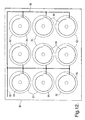
- FIG 12 illustrates a substrate 80 on which are formed a plurality of targets 82.
- each of the targets 82 is illustrated as having a spiral magnetic target track 84, this is merely exemplary, as any size and shape target or a plurality of target tracks can be formed according to the present invention.
- Each of the targets 82 and the spiral magnetic target tracks 84 are formed according to the steps set forth in conjunction with Figures 6 through 11, including a common conductor 86 electrically connected to the underlying copper trace of each target 82. Current is supplied to the copper traces through the common conductor 86 for electroplating the magnetic material over the copper traces, thereby forming the spiral magnetic target track 84. After formation of the spiral magnetic target tracks 84, the individual targets 82 are singulated.
- Figures 13 through 19 illustrate the process steps according to another embodiment of the present invention for forming magnetic targets, specifically an exemplary target 100 of Figure 13.
- the target 100 includes a magnetic target track 102 formed on a substrate 104.
- the magnetic target track 102 is shown in the shape of a spiral, this shape is merely exemplary.
- the cross-sectional views of Figures 14 through 19 are taken through the plane 14-14 of Figure 13.
- the substrate 104 such as FR-4 or ceramic, includes an overlaying copper layer 110.
- a relatively thin silver layer 112 is formed by any of the well-known deposition techniques over the copper layer 110.
- a photoresist layer 114 preferably of photoresist material SU-8 available from MicroChem Corporation of Newton, Massachusetts, is applied over the silver layer 112. See Figure 15.
- the SU-8 photoresist has a relatively high mechanical strength in the cross-linked state, i.e., after exposure to ultraviolet light, and can be applied in a layer sufficiently thick to allow the formation of high-aspect ratio targets (i.e., targets that are relatively thick compared to their width dimension).
- high-aspect ratio targets i.e., targets that are relatively thick compared to their width dimension.
- Other photoresist materials are suitable substitutes for SU-8 in the process of the present invention.
- a mask 116 is then introduced over the substrate 104, where the mask includes regions of varying opacity that define the desired target shape. Since the SU-8 photoresist material is a negative-acting photoresist, a trench to be formed within the photoresist layer 114 according to the present invention, is defined by opaque regions 118 in the mask 116. As can be seen from the top view of Figure 13, the magnetic target track 102 is a continuous structure. Thus the cross-sectional view of Figure 16 illustrates two spaced apart trenches in which the magnetic target track 102 is formed according to subsequent processing steps.
- the substrate 104 is exposed to ultraviolet light through the mask 116, as indicated by the arrowheads 120 in Figure 16.
- the photoresist layer is defined by certain exposed regions 122 exposed to the ultraviolet light passing through mask 116, and certain unexposed areas 124 blocked from ultraviolet light by the opaque regions 118.
- the exposed regions 122 are transformed from a relatively soluble state to a relatively insoluble state by the polymerization process caused by ultraviolet light.
- the unexposed regions 124 remain relatively soluble.
- the target region i.e., area where the trenches are to be formed
- the target region is defined by a transparent region in the mask 116 and the remainder of the mask 116 is opaque.
- a chemical developing material such as xylene, is then applied to the substrate 104 to remove the soluble unexposed regions 124, thereby forming trenches 130 in the photoresist layer 114.
- a chemical developing material such as xylene
- any number and size trenches can be formed as dictated by the specific geometry of the target track configurations, such as the target tracks illustrated in Figures 1, 2B and 4A.
- the substrate 104 is then immersed in a bath of an appropriate magnetic metal for electroplating the magnetic material in the trenches 130.
- Materials such as Cunife, Cunico, or Platinum-cobalt, as discussed above, are considered suitable candidates.
- the electroplating process During the electroplating process, current is supplied to the copper layer 110 or the silver layer 112, such that the silver layer 112 serves as the electroplating electrode, causing the magnetic material in the bath to fill the trenches 130 up from the silver layer 112, thereby forming target track segments 132. See Figure 18. When viewed from the top view of Figure 13, the target track segments 132 form the magnetic target track 102.
- the electroplating process is terminated when the top surface of the magnetic material in the trench 130 reaches the top surface of the photoresist layer 114.
- the substrate 104 is removed from the electroplating bath, washed, rinsed and dried.
- a protective passivation layer 138 is disposed over the target track segments 132 and the photoresist layer 114 to provide protection from mechanical and environmental degradation.
- the passivation layer 138 is formed by, for example, depositing polyimide or a similar polymeric compound.
- a second layer of the SU-8 material can be deposited to serve as the passivation layer 138.
- chromium can be electroplated over the target track segments 132 to form the passivation layer.
- the magnetic material of the magnetic target track 102 is magnetized by the application of a strong magnetizing force.
- the magnetic material of the magnetic track 102 can be magnetized either parallel or perpendicular to the plane of the substrate 104, depending on the type and orientation of the magnetic field sensor that will be employed with the target 100.
- the trench sidewalls provide mechanical strength and support for the target track.
- the underlying cooper and silver layers 110 and 112, respectively, provide a firm anchor for the target track. This lateral and underlying support is especially important for narrow target tracks and those having a high aspect ratio, i.e., depth with respect to width.
- the silver layer 112 provides mechanical bonding between the cured photoresist layer 114 and the underlying copper layer 110.
- the silver layer 112 is absent.
- the copper layer 110 is preferably carefully cleaned before application of the photoresist layer 114 to ensure a strong bond between the copper layer 110 and the photoresist layer 114, and also between the copper layer 110 and the later formed magnetic material.
- the silver layer 112 may be unnecessary in those embodiments where a photoresist material other than SU-8 is used as the material of the photoresist layer 114.
- FIG 20 illustrates a substrate 150 on which are formed a plurality of targets 152.
- each of the targets 152 is illustrated as having a spiral magnetic target track 154, this is merely exemplary, as any size and shape target can be formed according to this embodiment of the present invention.
- Each of the plurality of targets 152 and the magnetic target tracks 154 are formed according to the steps set forth in conjunction with Figures 14 through 19.
- the common conductor 86 is not required in this embodiment as electroplating current is supplied to deposit magnetic material in the trenches 130 through the copper layer 110 and/or the silver layer 112. After formation of the target tracks 154, the individual targets 152 are singulated.
- targets can be fabricated according to yet another process in which the copper cladding on a printed circuit board (such as the copper layer 110 of Figure 14) is replaced by a cladding of magnetic material, such as Cunife comprising about 60% copper, 20% nickel and 20% iron.
- the Cunife material which is available in thin sheets or foils, is a mechanically soft alloy that is further characterized by magnetically hard properties. Hoskins Manufacturing Company of Hamburg, MI is a supplier of the material.
- Cunife is laminated on printed circuit board substrates to form an assembly that can be patterned and etched according to known techniques. Appropriate etchants for these magnetic claddings are known, including ferric chloride (FeCl 3 ).
- a magnetic cladding material layer 220 is disposed over a base material or substrate 222, formed from a rigid polymer, ceramic, printed circuit board base material such as FR-4, or even a nonmagnetic metal (e.g., aluminum).
- the magnetic layer 220 comprises a material capable of exhibiting permanent magnetic properties, such as Cunife referred to above.
- a conventional photoresist material layer 226 is applied over the magnetic layer 220 as illustrated in Figure 22.
- a mask 228 is then introduced above the assembly, where the mask 228 includes regions of varying opacity, including an opaque region 229 that defines the desired target shape.
- the pattern of the mask 228 is transferred to the photoresist material layer 226 according to conventional printed circuit board processing techniques, by curing exposed regions of the photoresist material layer 226 and rendering these exposed regions soluble in a developer.
- Exposure to ultraviolet light, identified by arrowheads 230 is one known technique for transferring the mask pattern to create an unexposed region 232 in the photoresist material layer 226, where the unexposed region 232 is insoluble in the developer.
- a chemical developer such as xylene, is applied to the assembly to remove the soluble areas of the photoresist material layer 226, leaving only a photoresist mesa region 234. See Figure 24.
- the exposed regions of the magnetic layer 220 i.e., those regions over which the photoresist material layer 226 has been removed
- a printed circuit board etch chemistry such as ferric chloride (FeCl 3 .) can be used to remove regions of the magnetic layer 220.
- a target mesa region 238 remains above the substrate 222.
- the overlaying photoresist mesa region 234 is then removed, leaving the target mesa region 238 as shown in Figure 26.
- a passivation layer (not shown in Figure 26) is preferred to protect the Cunife target from environmental effects.
- Suitable passivation layer materials include a thin layer of nickel, chromium, or certain polymer materials.
Landscapes
- Engineering & Computer Science (AREA)
- Power Engineering (AREA)
- Manufacturing & Machinery (AREA)
- Physics & Mathematics (AREA)
- General Physics & Mathematics (AREA)
- Hall/Mr Elements (AREA)
- Transmission And Conversion Of Sensor Element Output (AREA)
- Physical Vapour Deposition (AREA)
Abstract
Description
- The present invention relates generally to position sensors, and more specifically to a method for forming permanent magnet targets for position sensors that provide the required degree of accuracy and resolution of the sensed position, and target apparatus formed thereby.
- Position sensors monitor the position or motion of a first mechanical component relative to a second mechanical component, by producing an electrical signal that varies as a function of the relative position of the two components. The relative speed of the two components can also be determined by taking the time derivative of the position Electrical position sensors are an important part of innumerable products, and are useful for determining the status of various automotive actuations and processes that involve either linear or angular displacement. For example, the position of an adjustable automotive seat can be determined by sensing devices mounted in the movable seat frame and the fixed seat guiding rails. The position and the angular velocity of the automotive engine crankshaft can also be determined by the appropriate placement of position sensing devices.
- One prior art position sensor, a contacting position sensor, requires physical contact between a signal generator and a sensing element to produce the electrical signal representative of position. Contacting position sensors typically consist of a potentiometer responsive to the signal generator and mechanically responsive to the component position, such that the output electrical signals vary as a function of the component's position. Motion-induced contact wear limits the durability of the contact-type position sensors.
- Non-contact magnetic type position sensors determine position by measuring changes in a magnetic field. Ferromagnetic material disposed on a moving object passes through a constant magnetic field, modulating the field in accordance with the object's position. One example of such a magnetic sensor includes a ferromagnetic target wheel attached to a rotating axle, the speed and/or position of which is to be determined. In one exemplary embodiment the target wheel comprises a plurality of ferromagnetic teeth defining slots therebetween. The constant magnetic field is produced by a stationary biasing magnet (conventionally a permanent magnet) positioned adjacent to the periphery of the target wheel. A magnetic field sensitive device, such as a magnetoresistor is mounted on the stationary magnet for measuring the magnetic field developed by the stationary magnetic, as modulated by the target wheel ferromagnetic teeth. As the wheel rotates the teeth pass adjacent the stationary magnet, changing the reluctance of the magnetic circuit and in turn varying the magnetic flux density of the magnetic field produced by the stationary magnet. These variations are sensed by the magnetoresistor and manifested as variations in the resistance thereof.
- Electronic circuitry responsive to the magnetoresistor produces an analog signal that varies in response to the magnetic field flux density variations. Thus a voltage signal in the form of a DC-biased waveform is produced. The waveform characteristics correspond to the shape and spacing of the teeth. When the signal exceeds a predetermined threshold, a tooth in the wheel has been detected adjacent the magnetoresistor. By appropriately spacing the teeth along the target wheel, the angular position of the rotating shaft can be determined. The angular velocity can also be determined as the rate of change of the position. It is known that the resistance of the magnetoresistor, and thus the position accuracy of such a device, is affected by the temperature, the air gap, magnet aging and the positional accuracy of the teeth relative to the rotating shaft.
- A Hall effect device can be used in lieu of a magnetoresistor to sense the changing magnetic field and provide an output signal in response thereto. As is known, a Hall effect device comprises a current-carrying conductor that when placed in a magnetic field such that the magnetic field flux lines are perpendicular to the direction of current flow, generates a voltage across the device that is perpendicular to both the direction of current flow and the magnetic flux lines. Thus the Hall effect voltage, which is a function of the magnetic field flux density, serves as a position indicator for a ferromagnetic target.
- Whether a magnetoresistor or a Hall effect device is utilized to sense the magnetic field and thus the object position, the position sensor must be accurate, in that it must produce an electrical signal based upon the measured position. An inaccurate position sensor hinders the proper position evaluation and control of the moving component. A position sensor must also be sufficiently precise in its measurement, although the degree of precision required depends upon the specific application. For some applications, only a rough indication of position is necessary. For instance, an indication of whether a valve is substantially opened or closed may be sufficient in some situations. In other applications a more precise indication of the valve position may be required. The position sensor must also be sufficiently durable for the environment in which it is placed. For example, a position sensor used on an automotive engine valve will experience almost constant movement while the automobile is in operation. The position sensor must be constructed of mechanical and electrical components that allow it to remain sufficiently accurate and precise during its projected lifetime, despite considerable mechanical vibrations and thermal extremes and gradients.
- The ferromagnetic targets discussed above are typically large and heavy structures, e.g., gears and slotted disks, manufactured by machining, stamping, blanking, powder metal technology, etc. These manufacturing methods are not only expensive, but are also not suitable for manufacturing targets with fine features and complex geometries that are required for high-accuracy small target sensors. Asymmetries in the placement of the teeth in a target wheel or changes in gap distance as the target wheel rotates cause inaccuracies in position determination.
- Targets with precise features are particularly needed in state-of-the-art continuous linear and angular position sensors. Such continuous sensors determine position continuously over a range of values, such as angular rotation between 0° to 120°. By comparison, the toothed wheel sensors described above provide discrete position indications when a tooth passes adjacent the field sensing element. The continuous sensors employ a single shaped target where the shape is designed to produce continuous variations in the magnetic field as the target moves relative to the sensor. A spiral shape is one example of a continuous target. Although it is possible to manufacture precise continuous sensors using the prior art techniques of machining, stamping, etc. described above, precision equipment is required and thus the cost for such sensors is high.
- One technique for forming precise ferromagnetic sensor targets is described and claimed in the commonly-owned patent application entitled, Method for Forming Ferromagnetic Targets for Position Sensors, filed on August 6, 2002, and assigned
application number 10/214,047. According to this method, photolithographic techniques allow for the formation of features as small as 0.1 mm by 0.1 mm, and up to about 1 mm thick for use with either discrete target or continuous target sensors. The magnetic field variations caused by targets with these dimensions can be sensed across air gaps in the range of about 0.25 to 0.5 mm, a range that is typical for high-accuracy position and speed sensors employed in most automotive systems. - The present invention teaches a method for manufacturing high accuracy permanent magnet targets for position and speed sensors using conventional printed circuit board manufacturing processes to produce precisely located, shaped and dimensioned target tracks.
- The target comprises a conductive layer disposed on an insulator substrate. A photoresist layer is formed over the conductive layer, and patterned and etched to form a trench therein. The photoresist trench is filled with a material that is subsequently magnetized to form the target track.
- The target is employed with a magnetic field sensor that produces an output signal representative of the position of the magnetic field (without the use of a bias magnet as required by the prior art), which is in turn representative of the position of the target track. The precision of the position detection is improved by the target track's straight vertical sidewalls and the precise positioning of the target resulting from use of the photolithographic process.
- The present invention will now be described, by way of example, with reference to the accompanying drawings in which
- Figure 1 illustrates a sensor target constructed according to the teachings of the present invention;
- Figures 2A and 2B illustrate an application of the sensor target of Figure 1;
- Figure 3 illustrates the sensor output for the sensor target of Figures 2A and 2B;
- Figures 4A and 4B illustrate another embodiment of a sensor target;
- Figure 5 illustrates the sensor output for the sensor target of Figures 4;
- Figures 6 through 11 illustrate the processing steps for manufacturing a sensor target, such as the sensor target of Figure 1, according to the teachings of a first embodiment of the present invention;
- Figure 12 illustrates a plurality of sensor targets fabricated according to the processing steps of Figures 6 through 11;
- Figures 13 through 19 illustrate the processing steps for manufacturing a sensor target according to a second embodiment of the present invention; and
- Figure 20 illustrates a plurality of sensor targets fabricated according to the processing steps of Figures 13 through 19;
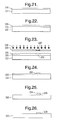
- Figures 21 through 26 illustrate the processing steps for manufacturing a sensor target according to a third embodiment of the present invention.
-
- Before describing in detail the particular method for forming targets for position and speed sensors and targets formed according to said methods in accordance with the teachings of the present invention, it should be observed that the present invention resides primarily in a novel and non-obvious combination of hardware elements and process steps related to forming said targets. Accordingly, the hardware elements and method steps have been represented by conventional elements in the specification and the drawings, showing only those specific details that are pertinent to the present invention, so as not to obscure the disclosure with structural details that will be readily apparent to those skilled in the art having the benefit of the description herein.
- Advantageously, according to the teachings of the present invention, the target includes permanent magnetic material in lieu of the prior art ferromagnetic material. The magnetic field sensing can be performed by a Hall effect device, a magnetoresistor, etc., from which the target position information is derived. However, the prior art bias magnet is not required, avoiding the cost of packaging the magnetic sensing element with the bias magnet and reducing the size of the sensing assembly. State-of-the-art position and speed sensors providing the required accuracy and resolution of the target position can be formed according to the present invention. Each target geometry can be designed for the intended application and must be formed with a sufficient quantity of magnetic material for sensing by conventional magnetic sensing devices, taking into consideration the air gap dimensions in use in many automotive and industrial applications.
- According to prior art techniques, the formation of permanent magnet targets can be costly and is generally limited to simple geometries formed from discrete multipole magnets or bulk permanent magnets. These techniques are not capable of satisfying the high accuracy requirements of today's state-of-the-art position and speed sensors.
- Figure 1 illustrates a target 8 comprising a continuous
magnetic target track 10 formed of a magnetic material on a copper-cladsubstrate material 12. In one embodiment, the completed assembly is coated with a passivation layer to protect thetarget track 10 from degradation caused by environmental effects. When such a magnetic target track is formed according to the teachings of the present invention, the accuracy and precision obtained is better than that available using the prior art methods. - An application of the target 8 for determining the angular position of a
rotating shaft 13 to which the target 8 is attached, is illustrated in Figures 2A and 2B. In particular, these Figures indicate an angular sensor that employs the spiralmagnetic target track 10 to generate an output signal proportional to the angle α, as illustrated in Figure 3. Amagnetic field sensor 15, such as a Hall effect device or a magnetoresistor, is mounted adjacent the target 8 for sensing the magnetic field of the spiralmagnetic target track 10. - By way of example, as shown in Figure 3, the spiral
magnetic target track 10 provides an output that is a linear function of the angle of rotation α. In another embodiment, the output value can be obtained from a microprocessor-controlled lookup table, where the index into the table is the angular position. Because precision targets can be formed according to the teachings of the present invention, in yet another embodiment the look-up table and the microprocessor are unnecessary, as the desired relationship between the target track position and the sensor output value can be provided directly by themagnetic field sensor 15 by appropriate design of the shape and dimensions of thetarget track 10. - Figures 4A and 4B illustrate another embodiment of a position sensor to which the teachings of the present invention can be applied. In Figure 4A planar complementary
magnetic targets target disk 19. The magnetic field of thetargets magnetic field sensors 21 and 22, respectively, shown in the side view of Figure 4B. Due to the discrete configuration of thetargets - Figures 6 through 11 illustrate the process steps according to the present invention for forming magnetic targets such as the spiral
magnetic target track 10 and the complementary magnetic target tracks 17 and 18 described above. Generally, the process employs conventional printed circuit board processing steps with variations to accommodate the formation of the target tracks comprising magnetically hard material. Magnetically hard materials exhibit a high coercivity (a measure of the opposition to the permanent magnetization or demagnetization of the material). A very strong magnetizing force must be supplied to the magnetically hard material to align the domains and create a permanent magnet. However, once the domains have been aligned, the magnetically hard material becomes a permanent magnet with ambient temperature and conditions having little or no disrupting effects on the magnet's properties. - Exemplary magnetically hard materials for use according to the teachings of the present invention include: Cunife, typically comprising 60% copper, 20% nickel and 20% iron, Cunico, typically comprising 50% copper, 20% nickel and 30% cobalt, and Platinum-cobalt, typically comprising 78% platinum and 22% cobalt. The latter material is especially suitable for use in micro-magnets employed in MEMS (i.e., micro-electro-mechanical systems) devices.
- The percentages of the elements comprising Cunife can be altered to optimize various magnetic properties of the material, such as the coercive force, residual induction, etc. A magnetically soft form of Cunife can also be formed, thus allowing the formation of complex magnetic circuits employing both hard and soft magnetic materials according to the teachings of the present invention.
- As illustrated in the side view of Figure 6, a
substrate 40, comprising conventional printed circuit board material such as FR-4 or ceramic, includes anoverlying copper layer 42. Thecopper layer 42 is patterned and etched to form traces 44 and 46 according to known conventional printed circuit board processing techniques. The resulting structure is illustrated in Figure 7. Photoresist applied to thetraces traces 44 may be thoroughly cleaned before formation of the magnetic material over thetraces 44, as described below, to ensure a high quality bond between the trace material and the magnetic material. - A
target 50 formed according to the process steps described in conjunction with Figures 6 and 7 is illustrated in Figure 8, where the cross-section line 7-7 identifies the plane along which Figure 7 is viewed. Thus thetraces 44 represent segments of aspiral target track 52 of thetarget 50. Thetrace 46 carries current during the electroplating process for thetarget 50 as described further below. - In lieu of the
copper layer 42, a copper clad ceramic material can also be employed as thecopper layer 42. Although the process is described for forming a spiral shaped magnetic target, the process is more generally applicable to any magnetic target size or shape. - In Figure 9, a protective
polymer coating layer 60 is deposited over thetrace 46 to prevent the plating thereof during the subsequent electroplating step. This deposition step can be executed by silk screening or stencil printing techniques that are conventional in printed circuit board processing. In another embodiment, the deposition step can be omitted, but thetrace 46 will be then electoplated in the next step and may thus interfere with operation of the magnetic field sensor. In still another embodiment, thepolymer layer 60 may not necessarily be required as thetrace 46 may be sufficiently distant from the useable portion of thetarget track 52 such that interference during the sensing process is precluded. - As illustrated in Figure 10, the
traces 44 are electroplated with a layer comprising one of the various permanent magnetic materials described above, or another permanent known magnetic material known in the art. Current for the electroplating process is carried over thetrace 46 to thetraces 44. As is known to those skilled in the art, the electroplating process is carried out by immersing thesubstrate 40 in a bath of solution including the magnetic material while supplying the aforementioned current. The electroplating process results in the formation of the magneticspiral target track 52 illustrated in Figure 8. - To prevent corrosion and environmental degradation of the magnetic material of the
target track 52, a thin passivation barrier layer (not shown in Figure 10) of chromium, nickel or a polymeric material can be formed over the magnetic material. - A
passivation layer 70, illustrated in Figure 11 can be applied to theentire target 50 to provide a barrier against harmful environmental effects. Suitable passivation materials include various polymeric compounds. - The magnetic material forming the
track 52 is magnetized by the application of a strong magnetizing force. The magnetic material can be magnetized either parallel or perpendicular to the plane of thesubstrate 40, depending on the characteristics and orientation of the magnetic field sensor that will be employed with thetarget 50. - Although the process according to the present invention has been explained above in conjunction with the fabrication of a
single target track 52, a plurality of such targets, such as the planar complementarymagnetic targets - To improve the efficiency of the fabrication process, a plurality of such targets can be formed simultaneously on a single sheet of substrate material.
- Figure 12 illustrates a
substrate 80 on which are formed a plurality oftargets 82. Although each of thetargets 82 is illustrated as having a spiralmagnetic target track 84, this is merely exemplary, as any size and shape target or a plurality of target tracks can be formed according to the present invention. Each of thetargets 82 and the spiral magnetic target tracks 84 are formed according to the steps set forth in conjunction with Figures 6 through 11, including acommon conductor 86 electrically connected to the underlying copper trace of eachtarget 82. Current is supplied to the copper traces through thecommon conductor 86 for electroplating the magnetic material over the copper traces, thereby forming the spiralmagnetic target track 84. After formation of the spiral magnetic target tracks 84, theindividual targets 82 are singulated. - Figures 13 through 19 illustrate the process steps according to another embodiment of the present invention for forming magnetic targets, specifically an exemplary target 100 of Figure 13. The target 100 includes a
magnetic target track 102 formed on asubstrate 104. Although themagnetic target track 102 is shown in the shape of a spiral, this shape is merely exemplary. The cross-sectional views of Figures 14 through 19 are taken through the plane 14-14 of Figure 13. - Referring to Figure 14, the
substrate 104, such as FR-4 or ceramic, includes an overlayingcopper layer 110. A relativelythin silver layer 112 is formed by any of the well-known deposition techniques over thecopper layer 110. - According to the teachings of the present invention, a
photoresist layer 114, preferably of photoresist material SU-8 available from MicroChem Corporation of Newton, Massachusetts, is applied over thesilver layer 112. See Figure 15. The SU-8 photoresist has a relatively high mechanical strength in the cross-linked state, i.e., after exposure to ultraviolet light, and can be applied in a layer sufficiently thick to allow the formation of high-aspect ratio targets (i.e., targets that are relatively thick compared to their width dimension). Other photoresist materials are suitable substitutes for SU-8 in the process of the present invention. - A
mask 116 is then introduced over thesubstrate 104, where the mask includes regions of varying opacity that define the desired target shape. Since the SU-8 photoresist material is a negative-acting photoresist, a trench to be formed within thephotoresist layer 114 according to the present invention, is defined byopaque regions 118 in themask 116. As can be seen from the top view of Figure 13, themagnetic target track 102 is a continuous structure. Thus the cross-sectional view of Figure 16 illustrates two spaced apart trenches in which themagnetic target track 102 is formed according to subsequent processing steps. - The
substrate 104 is exposed to ultraviolet light through themask 116, as indicated by thearrowheads 120 in Figure 16. After exposure the photoresist layer is defined by certain exposedregions 122 exposed to the ultraviolet light passing throughmask 116, and certainunexposed areas 124 blocked from ultraviolet light by theopaque regions 118. The exposedregions 122 are transformed from a relatively soluble state to a relatively insoluble state by the polymerization process caused by ultraviolet light. Theunexposed regions 124 remain relatively soluble. - In another embodiment, where a positive-acting photoresist material is used, the target region (i.e., area where the trenches are to be formed) is defined by a transparent region in the
mask 116 and the remainder of themask 116 is opaque. - A chemical developing material, such as xylene, is then applied to the
substrate 104 to remove the solubleunexposed regions 124, thereby formingtrenches 130 in thephotoresist layer 114. Although only two trenches are shown in Figure 17 according to the spiralmagnetic track 102 shown in Figure 13, it is known that any number and size trenches can be formed as dictated by the specific geometry of the target track configurations, such as the target tracks illustrated in Figures 1, 2B and 4A. - The
substrate 104 is then immersed in a bath of an appropriate magnetic metal for electroplating the magnetic material in thetrenches 130. Materials such as Cunife, Cunico, or Platinum-cobalt, as discussed above, are considered suitable candidates. - During the electroplating process, current is supplied to the
copper layer 110 or thesilver layer 112, such that thesilver layer 112 serves as the electroplating electrode, causing the magnetic material in the bath to fill thetrenches 130 up from thesilver layer 112, thereby formingtarget track segments 132. See Figure 18. When viewed from the top view of Figure 13, thetarget track segments 132 form themagnetic target track 102. The electroplating process is terminated when the top surface of the magnetic material in thetrench 130 reaches the top surface of thephotoresist layer 114. - The
substrate 104 is removed from the electroplating bath, washed, rinsed and dried. As shown in Figure 19, aprotective passivation layer 138 is disposed over thetarget track segments 132 and thephotoresist layer 114 to provide protection from mechanical and environmental degradation. Thepassivation layer 138 is formed by, for example, depositing polyimide or a similar polymeric compound. In another embodiment, a second layer of the SU-8 material can be deposited to serve as thepassivation layer 138. In yet another embodiment, chromium can be electroplated over thetarget track segments 132 to form the passivation layer. - As discussed above with respect to the previous embodiment, the magnetic material of the
magnetic target track 102 is magnetized by the application of a strong magnetizing force. The magnetic material of themagnetic track 102 can be magnetized either parallel or perpendicular to the plane of thesubstrate 104, depending on the type and orientation of the magnetic field sensor that will be employed with the target 100. - By forming the magnetic target track within a
photoresist trench 130, the trench sidewalls provide mechanical strength and support for the target track. Also, the underlying cooper andsilver layers - The
silver layer 112 provides mechanical bonding between the curedphotoresist layer 114 and theunderlying copper layer 110. However, in another embodiment not shown in the Figures, thesilver layer 112 is absent. In this embodiment thecopper layer 110 is preferably carefully cleaned before application of thephotoresist layer 114 to ensure a strong bond between thecopper layer 110 and thephotoresist layer 114, and also between thecopper layer 110 and the later formed magnetic material. In particular, thesilver layer 112 may be unnecessary in those embodiments where a photoresist material other than SU-8 is used as the material of thephotoresist layer 114. - Figure 20 illustrates a
substrate 150 on which are formed a plurality oftargets 152. Although each of thetargets 152 is illustrated as having a spiralmagnetic target track 154, this is merely exemplary, as any size and shape target can be formed according to this embodiment of the present invention. Each of the plurality oftargets 152 and the magnetic target tracks 154 are formed according to the steps set forth in conjunction with Figures 14 through 19. As compared to the embodiment with thecommon conductor 86 as referred to in Figure 12 above, thecommon conductor 86 is not required in this embodiment as electroplating current is supplied to deposit magnetic material in thetrenches 130 through thecopper layer 110 and/or thesilver layer 112. After formation of the target tracks 154, theindividual targets 152 are singulated. - In another embodiment of the present invention, targets can be fabricated according to yet another process in which the copper cladding on a printed circuit board (such as the
copper layer 110 of Figure 14) is replaced by a cladding of magnetic material, such as Cunife comprising about 60% copper, 20% nickel and 20% iron. The Cunife material, which is available in thin sheets or foils, is a mechanically soft alloy that is further characterized by magnetically hard properties. Hoskins Manufacturing Company of Hamburg, MI is a supplier of the material. Cunife is laminated on printed circuit board substrates to form an assembly that can be patterned and etched according to known techniques. Appropriate etchants for these magnetic claddings are known, including ferric chloride (FeCl3). - As shown in Figure 21, a magnetic cladding material layer 220 is disposed over a base material or
substrate 222, formed from a rigid polymer, ceramic, printed circuit board base material such as FR-4, or even a nonmagnetic metal (e.g., aluminum). The magnetic layer 220 comprises a material capable of exhibiting permanent magnetic properties, such as Cunife referred to above. A conventionalphotoresist material layer 226 is applied over the magnetic layer 220 as illustrated in Figure 22. - As shown in Figure 23, a
mask 228 is then introduced above the assembly, where themask 228 includes regions of varying opacity, including anopaque region 229 that defines the desired target shape. The pattern of themask 228 is transferred to thephotoresist material layer 226 according to conventional printed circuit board processing techniques, by curing exposed regions of thephotoresist material layer 226 and rendering these exposed regions soluble in a developer. Exposure to ultraviolet light, identified byarrowheads 230, is one known technique for transferring the mask pattern to create anunexposed region 232 in thephotoresist material layer 226, where theunexposed region 232 is insoluble in the developer. - A chemical developer, such as xylene, is applied to the assembly to remove the soluble areas of the
photoresist material layer 226, leaving only aphotoresist mesa region 234. See Figure 24. The exposed regions of the magnetic layer 220 (i.e., those regions over which thephotoresist material layer 226 has been removed) are removed by use of an appropriate etchant. In the embodiment where the magnetic layer 220 comprises Cunife, a printed circuit board etch chemistry such as ferric chloride (FeCl3.) can be used to remove regions of the magnetic layer 220. After removal of the exposed regions of the magnetic layer 220, atarget mesa region 238 remains above thesubstrate 222. The overlayingphotoresist mesa region 234 is then removed, leaving thetarget mesa region 238 as shown in Figure 26. - In one embodiment, a passivation layer (not shown in Figure 26) is preferred to protect the Cunife target from environmental effects. Suitable passivation layer materials include a thin layer of nickel, chromium, or certain polymer materials. Finally, the
Cunife target 238 is magnetized as described above. - While the invention has been described with reference to preferred embodiments, it will be understood by those skilled in the art that various changes may be made and equivalent elements may be substituted for elements thereof without departing from the scope of the present invention. The scope of the present invention further includes any combination of the elements from the various embodiments set forth herein. In addition, modifications may be made to adapt a particular situation to the teachings of the present invention without departing from its essential scope thereof. For example, differently sized and shaped targets than those illustrated can be formed according to the teachings of the present invention. Therefore, it is intended that the invention not be limited to the particular embodiment disclosed as the best mode contemplated for carrying out this invention, but that the invention will include all embodiments falling within the scope of the appended claims.
Claims (34)
- A method for forming a target 100 comprising a magnetic target track 102 on a substrate 104, comprising:forming a conductive layer 110 on the substrate 104;disposing a photoresist layer 114 over the conductive layer 110;forming at least one trench 130 in the photoresist layer 114, wherein the at least one trench 130 is in the shape of the magnetic target track 102;forming magnetic material 132 in the trench 102; andmagnetizing the magnetic material 132 to form the magnetic target track 102.
- The method of claim 1 wherein the material of the conductive layer 110 comprises copper.
- The method of claim 1 wherein the photoresist layer 114 comprises a negative-acting photoresist.
- The method of claim 3 wherein the negative acting photoresist 114 comprises SU-8.
- The method of claim 1 wherein the step of patterning further comprises:positioning a photolithographic mask 116 over the photoresist layer 114, wherein the mask 116 includes one or more relatively transparent and one or more relatively opaque regions 118;exposing the mask 116 to radiation 120, causing the regions of the photoresist layer 114 subjected to the radiation 120 to undergo a structural change; andetching regions of the mask 116, wherein the etched regions 130 comprise the regions that underwent a structural change or the regions that did not undergo a structural change to form the at least one trench 130 therein.
- The method of claim 1 wherein the step of forming the magnetic material 132 in the trench 130 comprises immersing the substrate in an electroplating bath of magnetic material 132, providing an electrical current through the conductive layer 110 and electroplating the magnetic material 132 in the trench 130 to form the magnetic material 132.
- The method of claim 1 wherein a plurality of targets 152 are formed simultaneously on a common substrate 150.
- The method of claim 7 wherein the conductive layer 110 is common to each of the plurality of targets 152 for receiving electrical current during the electroplating step such that the magnetic material 132 is simultaneously formed in the at least one trench of each one of the plurality of targets.
- The method of claim 7 further comprising singulating the plurality of targets 152.
- The method of claim 1 wherein the magnetic material 132 is selected from among Cunife, Cunico and platinum-cobalt.
- The method of claim 1 further comprising forming a passivation layer 70 over the target 100.
- The method of claim 1 wherein the substrate 104 is attached to a moving object 13, and wherein a sensor 21/22 determines one or more of the position, velocity, speed and acceleration of the moving object 13 in response to the magnetic field produced by the magnetic target track 102.
- A method for forming a target 50 comprising a magnetic target track 52 on a substrate 40, wherein the substrate 40 comprises an underlying dielectric layer and an overlying conductive layer 42, said method comprising:patterning the conductive layer 42 by removing certain regions of the conductive layer, wherein the remaining regions form patterned conductive regions 44;forming magnetic material 62 on the patterned conductive regions; andmagnetizing the magnetic material to form the magnetic target track 52.
- The method of claim 13 wherein the conductive layer 42 comprises copper.
- The method of claim 13 wherein the step of patterning further comprises:applying a photoresist layer 114 over the conductive layer 42;positioning a mask 116 over the photoresist layer 114, wherein the mask 116 includes one or more relatively transparent regions and one or more relatively opaque regions 118;exposing the mask to electromagnetic radiation 120, causing the regions of the photoresist layer 114 subjected to the radiation to undergo a structural change; andremoving regions of the photoresist layer 114 to expose regions of the underlying conductive layer 42, wherein the removed regions comprise the regions that underwent a structural change or the regions that did not undergo a structural change, such that the remaining regions of the photoresist layer 114 overly the regions of the conductive layer 42 that define the patterned conductive regions 44;removing exposed regions of the conductive layer 42; andremoving the remaining regions of the photoresist layer 114 that overly the regions of the conductive layer 42 that define the patterned conductive regions 44.
- The method of claim 15 wherein the step of forming the magnetic material 62 further comprises electroplating magnetic material 62 on the patterned conductive regions 44 to form the magnetic target track 52.
- The method of claim 13 wherein a plurality of targets 82 are formed simultaneously on a common substrate 80.
- The method of claim 17 further comprising forming a common conductor 86 connecting each of the patterned conductive regions, wherein the common conductor serves as the common conductor during the electroplating step, such that magnetic material 62 is formed on each one of the patterned conductive regions 44 of the plurality of targets 82.
- The method of claim 18 further comprising forming a barrier layer 60 over the common conductor 86, such that during the step of forming the magnetic material 62 the barrier layer 60 prevents forming of the magnetic material 62 on the common conductor 86.
- The method of claim 13 wherein the magnetic material 62 is selected from among Cunife, Cunico and platinum-cobalt.
- A method for forming a target 50 comprising a magnetic target track 52 on a substrate 222, comprising:forming a magnetic layer 220 on the substrate 222; andpatterning the magnetic layer 220 to form at least one target 52 therein.
- A method for forming a target 50 comprising a magnetic target track 52 on a substrate 222, comprising:wherein the magnetic material 220 underlying the mesa region 234 forms the magnetic target track 52.forming a magnetic layer 220 on a substrate 222;forming a photoresist layer 114 over the magnetic layer 220;patterning the photoresist layer 114 to form at least one mesa region 234 therein;removing the magnetic layer 220 except in the regions underlying the at least one mesa region 234; and
- The method of claim 22 wherein the magnetic material 220 is selected from among Cunife, Cunico, and platinum-cobalt.
- The method of claim 23 further comprising magnetizing the magnetic material 220.
- The method of claim 22 further comprising removing the at least one mesa region 234.
- A magnetic target 100 comprising a magnetic target track 102 for a position sensor 8, comprising:a substrate 104;a conductive layer 110 overlaying said substrate 104;a dielectric layer overlaying said conductive layer 104, wherein said dielectric layer includes one or more trenches 130 in the shape of a target track 102; andmagnetic material 132 in the trench such that the material-filled trench forms the magnetic target track 102.
- The magnetic target 100 of claim 26 wherein the conductive layer 110 comprises copper.
- The magnetic target 100 of claim 26 wherein the dielectric layer comprises photoresist 114.
- A magnetic target 100 comprising a magnetic target track 102 for a position sensor 8, comprising:a substrate 104; anda patterned magnetic layer 220 overlying said substrate 104, wherein said patterned magnetic layer 220 forms said magnetic target track 102.
- A magnetic target 100 for a position sensor 8, comprising:a substrate 104;a patterned conductive layer 110 overlying said substrate 104;a magnetic layer 220 formed over said patterned conductive layer 110.
- A position sensor 8 comprising:a moving target 10 having magnetic material 132 formed therein;a magnetic field sensor 21/22 for sensing the magnetic field created by the magnetic material 132 and for detecting motion of the moving target 10 based thereon.
- The position sensor 8 of claim 31 wherein the target 10 comprises a substrate 104 and a dielectric layer 114 overlying said substrate, wherein the dielectric layer has one or more trenches 130 formed therein, and wherein the magnetic material 132 is formed in the one or more trenches 130.
- The position sensor 8 of claim 31 wherein the target 10 comprises a substrate 104 and a patterned layer of magnetic material 220 formed thereover.
- The position sensor 8 of claim 31 wherein the target 10 comprises a substrate 40, a patterned conductive material 44 formed thereover, and magnetic material 62 formed over the patterned conductive material.
Applications Claiming Priority (2)
| Application Number | Priority Date | Filing Date | Title |
|---|---|---|---|
| US372750 | 1982-04-28 | ||
| US10/372,750 US7062840B2 (en) | 2003-02-24 | 2003-02-24 | Method for forming permanent magnet targets for position sensors |
Publications (2)
| Publication Number | Publication Date |
|---|---|
| EP1450382A2 true EP1450382A2 (en) | 2004-08-25 |
| EP1450382A3 EP1450382A3 (en) | 2006-06-14 |
Family
ID=32736474
Family Applications (1)
| Application Number | Title | Priority Date | Filing Date |
|---|---|---|---|
| EP04075410A Withdrawn EP1450382A3 (en) | 2003-02-24 | 2004-02-10 | Method for forming permanent magnet targets for position sensors |
Country Status (2)
| Country | Link |
|---|---|
| US (1) | US7062840B2 (en) |
| EP (1) | EP1450382A3 (en) |
Cited By (1)
| Publication number | Priority date | Publication date | Assignee | Title |
|---|---|---|---|---|
| CN114473917A (en) * | 2022-03-09 | 2022-05-13 | 广西玉柴机器股份有限公司 | Crankshaft sensor support positioning tool |
Families Citing this family (12)
| Publication number | Priority date | Publication date | Assignee | Title |
|---|---|---|---|---|
| US7229746B2 (en) * | 2003-04-02 | 2007-06-12 | Delphi Technologies, Inc. | Printed high strength permanent magnet targets for magnetic sensors |
| TWM246600U (en) * | 2003-12-31 | 2004-10-11 | Taigene Metal Industry Co Ltd | Magnetic sensor |
| US20050212353A1 (en) * | 2004-03-25 | 2005-09-29 | Tolani Nirmal M | Corrosion and heat resistant coating for anti-lock brake rotor exciter ring |
| US20080136227A1 (en) * | 2006-12-11 | 2008-06-12 | 3M Innovative Properties Company | Vehicle seat sensor assembly |
| WO2015006454A1 (en) * | 2013-07-09 | 2015-01-15 | United Technologies Corporation | Non-contact strain measurement |
| CN105473956B (en) * | 2013-08-27 | 2018-07-31 | 丹佛斯公司 | A kind of compressor including stream controller and electromagnetic actuators |
| JP6311200B2 (en) * | 2014-06-26 | 2018-04-18 | 住友電工プリントサーキット株式会社 | Printed wiring board, electronic component, and printed wiring board manufacturing method |
| US9797268B2 (en) * | 2015-03-27 | 2017-10-24 | United Technologies Corporation | Oil scoop with integrated sensor |
| US10008325B2 (en) | 2015-06-08 | 2018-06-26 | Apple Inc. | Thin magnet fabrication |
| US11448524B2 (en) | 2016-04-07 | 2022-09-20 | Phoenix America Inc. | Multipole magnet for use with a pitched magnetic sensor |
| JP7323268B2 (en) * | 2018-03-16 | 2023-08-08 | 日東電工株式会社 | Magnetic wiring circuit board and manufacturing method thereof |
| EP3860317B1 (en) * | 2018-09-27 | 2024-07-24 | Denka Company Limited | Bonded substrate, metal circuit board, and circuit board |
Family Cites Families (18)
| Publication number | Priority date | Publication date | Assignee | Title |
|---|---|---|---|---|
| US3619285A (en) * | 1969-12-10 | 1971-11-09 | Rca Corp | Method of making a patterned metal film article |
| US4746580A (en) * | 1983-03-31 | 1988-05-24 | International Business Machines Corporation | Read-only magnetic recording media |
| US4670316A (en) * | 1983-05-11 | 1987-06-02 | General Electric Company | Thermo-magnetic recording materials supporting small stable domains |
| JPS62216110A (en) * | 1986-03-14 | 1987-09-22 | タツタ電線株式会社 | Variable pitch cable |
| US4835467A (en) | 1988-01-25 | 1989-05-30 | General Motors Corporation | Wheel speed sensor |
| US4924696A (en) | 1989-07-24 | 1990-05-15 | General Motors Corporation | Noncontacting position sensor for an automotive steering system |
| US5427675A (en) * | 1991-10-29 | 1995-06-27 | Teijin Seiki Co., Ltd. | Method of manufacturing article having magnetic patterns |
| US5754042A (en) | 1994-06-20 | 1998-05-19 | General Motors Corporation | Magnetoresistive encoder for tracking the angular position of a rotating ferromagnetic target wheel |
| JPH09153406A (en) * | 1995-09-28 | 1997-06-10 | Toshiba Corp | Planar coil, planar magnetic element using the same, and manufacturing method thereof |
| US5731702A (en) | 1996-08-21 | 1998-03-24 | General Motors Corporation | High accuracy angle based rotation sensor with time based back up |
| US6124709A (en) * | 1998-06-05 | 2000-09-26 | Cts Corporation | Magnetic position sensor having a variable width magnet mounted into a rotating disk and a hall effect sensor |
| US6304078B1 (en) | 1998-12-09 | 2001-10-16 | Cts Corporation | Linear position sensor |
| US6310473B1 (en) | 1998-12-15 | 2001-10-30 | Kearney-National, Inc. | Magnetic rotational position sensor |
| US6218080B1 (en) * | 2000-03-06 | 2001-04-17 | Headway Technologies, Inc. | Plated flat metal gap for very narrow recording heads |
| US6201466B1 (en) | 2000-03-29 | 2001-03-13 | Delphi Technologies, Inc. | Magnetoresistor array |
| US20040009614A1 (en) * | 2000-05-12 | 2004-01-15 | Ahn Chong H | Magnetic bead-based arrays |
| US6469497B2 (en) | 2001-01-09 | 2002-10-22 | Delphi Technologies, Inc. | Magnetic position sensor system composed of two reference magnetoresistors and a linear displacement sensing magnetoresistor |
| US6498482B2 (en) | 2001-01-18 | 2002-12-24 | Delphi Technologies, Inc. | Magnetoresistor die composed of two reference mangetoresistors and a linear displacement sensing magnetoresistor |
-
2003
- 2003-02-24 US US10/372,750 patent/US7062840B2/en not_active Expired - Fee Related
-
2004
- 2004-02-10 EP EP04075410A patent/EP1450382A3/en not_active Withdrawn
Non-Patent Citations (1)
| Title |
|---|
| None * |
Cited By (1)
| Publication number | Priority date | Publication date | Assignee | Title |
|---|---|---|---|---|
| CN114473917A (en) * | 2022-03-09 | 2022-05-13 | 广西玉柴机器股份有限公司 | Crankshaft sensor support positioning tool |
Also Published As
| Publication number | Publication date |
|---|---|
| US7062840B2 (en) | 2006-06-20 |
| US20040164730A1 (en) | 2004-08-26 |
| EP1450382A3 (en) | 2006-06-14 |
Similar Documents
| Publication | Publication Date | Title |
|---|---|---|
| US7229746B2 (en) | Printed high strength permanent magnet targets for magnetic sensors | |
| US7062840B2 (en) | Method for forming permanent magnet targets for position sensors | |
| US7969148B2 (en) | Magnetic sensor device, magnetic encoder device and magnetic scale manufacturing method | |
| US11293744B2 (en) | Method for increasing the position measurement accuracy using inductive position sensor | |
| CN100520303C (en) | Magnet sensor arrangement | |
| US8067934B2 (en) | Measurement device for measuring a magnetic field | |
| EP0419040A1 (en) | Speed/position sensor based upon magnetoresistive effect | |
| JP3065129B2 (en) | Movable ferromagnetic element detection device | |
| US7119539B2 (en) | Arrangement for determining the position of a motion sensor element | |
| US20040070390A1 (en) | Magnetic angular position sensor apparatus | |
| JPH06341853A (en) | Magnetic position sensor | |
| CA2399328A1 (en) | Non-contacting linear position sensor | |
| EP0390405B1 (en) | Magnetic sensor unit | |
| JP3367230B2 (en) | Position detection device | |
| JP3260921B2 (en) | Movable body displacement detection device | |
| JP6132085B2 (en) | Magnetic detector | |
| CN103454599A (en) | Magnetic field sensor | |
| US20040027846A1 (en) | Method for forming ferromagnetic targets for position sensors | |
| JP2000180524A (en) | Magnetic field sensor | |
| EP1264189A1 (en) | Arrangement for measuring the magnetic field strength | |
| US6687111B2 (en) | Electromagnetic mark device for a magnetism encoder | |
| WO2014073196A1 (en) | Magnetic detecting unit and stroke detecting device using magnetic detecting unit | |
| JP2008298729A (en) | Magnetic scale for magnetic type encoder and manufacturing method thereof | |
| JPH03282368A (en) | Magnetic sensor | |
| US20210348952A1 (en) | Sensor Unit for a Sensor/Transmitter System and a Sensor/Transmitter System Having Such a Sensor Unit |
Legal Events
| Date | Code | Title | Description |
|---|---|---|---|
| PUAI | Public reference made under article 153(3) epc to a published international application that has entered the european phase |
Free format text: ORIGINAL CODE: 0009012 |
|
| AK | Designated contracting states |
Kind code of ref document: A2 Designated state(s): AT BE BG CH CY CZ DE DK EE ES FI FR GB GR HU IE IT LI LU MC NL PT RO SE SI SK TR |
|
| AX | Request for extension of the european patent |
Extension state: AL LT LV MK |
|
| PUAL | Search report despatched |
Free format text: ORIGINAL CODE: 0009013 |
|
| AK | Designated contracting states |
Kind code of ref document: A3 Designated state(s): AT BE BG CH CY CZ DE DK EE ES FI FR GB GR HU IE IT LI LU MC NL PT RO SE SI SK TR |
|
| AX | Request for extension of the european patent |
Extension state: AL LT LV MK |
|
| 17P | Request for examination filed |
Effective date: 20061214 |
|
| AKX | Designation fees paid |
Designated state(s): DE FR GB |
|
| 17Q | First examination report despatched |
Effective date: 20070202 |
|
| STAA | Information on the status of an ep patent application or granted ep patent |
Free format text: STATUS: THE APPLICATION IS DEEMED TO BE WITHDRAWN |
|
| 18D | Application deemed to be withdrawn |
Effective date: 20070814 |