EP1450238A1 - Circuit for programmable stepless clock shifting - Google Patents
Circuit for programmable stepless clock shifting Download PDFInfo
- Publication number
- EP1450238A1 EP1450238A1 EP03290424A EP03290424A EP1450238A1 EP 1450238 A1 EP1450238 A1 EP 1450238A1 EP 03290424 A EP03290424 A EP 03290424A EP 03290424 A EP03290424 A EP 03290424A EP 1450238 A1 EP1450238 A1 EP 1450238A1
- Authority
- EP
- European Patent Office
- Prior art keywords
- clock
- sin
- ref
- cos
- splitter
- Prior art date
- Legal status (The legal status is an assumption and is not a legal conclusion. Google has not performed a legal analysis and makes no representation as to the accuracy of the status listed.)
- Granted
Links
Images
Classifications
-
- G—PHYSICS
- G06—COMPUTING OR CALCULATING; COUNTING
- G06F—ELECTRIC DIGITAL DATA PROCESSING
- G06F1/00—Details not covered by groups G06F3/00 - G06F13/00 and G06F21/00
- G06F1/04—Generating or distributing clock signals or signals derived directly therefrom
- G06F1/10—Distribution of clock signals, e.g. skew
-
- H—ELECTRICITY
- H03—ELECTRONIC CIRCUITRY
- H03K—PULSE TECHNIQUE
- H03K5/00—Manipulating of pulses not covered by one of the other main groups of this subclass
- H03K2005/00013—Delay, i.e. output pulse is delayed after input pulse and pulse length of output pulse is dependent on pulse length of input pulse
- H03K2005/00019—Variable delay
- H03K2005/00026—Variable delay controlled by an analog electrical signal, e.g. obtained after conversion by a D/A converter
-
- H—ELECTRICITY
- H03—ELECTRONIC CIRCUITRY
- H03K—PULSE TECHNIQUE
- H03K5/00—Manipulating of pulses not covered by one of the other main groups of this subclass
- H03K2005/00286—Phase shifter, i.e. the delay between the output and input pulse is dependent on the frequency, and such that a phase difference is obtained independent of the frequency
Definitions
- the present invention relates to a circuit for programmable stepless clock shifting.
- the associated clock In a number of situations, when transferring data between different chips, boards or devices, the associated clock is usually not distributed. The main reason is pin count reduction and power saving. At the receiving end, the problem of recovering the associated clock arises, in order to sample and process the incoming data stream. The operation of phase aligning often cannot be avoided also when the associated clock signal is distributed along with the data signal.
- DLL delay locked loops
- PLL phase locked loops
- DPA digital phase aligners
- PLL based solutions require considerable power and chip area and are generally not able to cope with a wide range data transition density or long CID (continuous identical digits) sequences, as often required by applications.
- a PLL is used to generate N phases of the reference clock. They are all distributed to each receiving macro in which one is selected in order to sample the incoming data. This solution requires a lot of area for the wiring.
- switching noise, variations in phase difference between the clock multiphases and duty cycle distortion become a challenging issue when covering a long path; in addition the mimimum distance in degrees between two adiacent phases is limited by the technology used for the chip.
- one PLL is used to generate one filtered clock phase which is then distributed to all the receiving macros. Locally all the phases are generated by means of a DLL. Power consumption and occupation area remain a severe issue. Also in these cases the mimimum distance in degrees between two adiacent phases is limited by the technology.
- DPA digital phase aligners
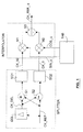
- the basic idea of the present invention is to provide a programmable stepless clock shifter, consisting of a splitter generating a 0° and a 90° shifted clocks from a reference clock, and an interpolator of this two phases, which provides at the output the desired pre-set clock phase.
- the solution consists of two blocks in series, a splitter (SPLITTER) and an interpolator (INTERPOLATOR): the splitter receives a clock CK_REF and generates two clock phases, 90° shifted; the interpolator uses these two clock phases and two coefficients SIN_ ⁇ and COS_ ⁇ , and produces a clock, which has a phase that depends only on the input coefficients.
- SPLITTER splitter
- INTERPOLATOR interpolator
- ⁇ 90° ⁇ 50%.
- This block receives the two 90° shifted clocks CK_90 and CK_0 from the splitter and provides a clock with a phase that is programmable by setting two appropriate input coefficients.
- the two 90° shifted clocks CK_90 and CK_0 are sent to respective inputs of two multipliers M1 and M2; the second input of M1 is supplied with a first coefficient SIN_ ⁇ and the second input of M2 with a second coefficient COS_ ⁇ .
- the outputs of M1 and M2 are supplied to the inputs of an adder S3 wich gives at the output the wanted clock reference CK_REF_ ⁇ with the pre-set phase difference ⁇ with respect to the input clock CK_REF.
- the two coefficients SIN_ ⁇ and COS_ ⁇ are selected in any wanted way.
- they can come from a memory table TAB suitably addressed, according to the wanted phase shift ⁇ , which can be any.
- the minimum angle between two adiacent phases is not technology nor temperature nor supply dependent.
- the resolution can be chosen as high as needed (stepless clock shifter).
- a monolitich chip implementation for example a VLSI technology, takes advantage of the low power consumption and the low silicon area required. No filter has to be implemented.
Landscapes
- Engineering & Computer Science (AREA)
- Theoretical Computer Science (AREA)
- Physics & Mathematics (AREA)
- General Engineering & Computer Science (AREA)
- General Physics & Mathematics (AREA)
- Stabilization Of Oscillater, Synchronisation, Frequency Synthesizers (AREA)
- Manipulation Of Pulses (AREA)
- Synchronizing For Television (AREA)
- Pulse Circuits (AREA)
Abstract
Description
Often a PLL is used to generate N phases of the reference clock. They are all distributed to each receiving macro in which one is selected in order to sample the incoming data. This solution requires a lot of area for the wiring. Besides, switching noise, variations in phase difference between the clock multiphases and duty cycle distortion become a challenging issue when covering a long path; in addition the mimimum distance in degrees between two adiacent phases is limited by the technology used for the chip.
- Fig. 1 shows a block diagram of the circuit in accordance with the invention.
The outputs of M1 and M2 are supplied to the inputs of an adder S3 wich gives at the output the wanted clock reference CK_REF_Φ with the pre-set phase difference Φ with respect to the input clock CK_REF.
Claims (7)
- Circuit for programmable stepless clock shifting, characterized in that it comprises:a splitter (SPLITTER), receiving a clock reference (CK_REF) and generating two 90°-shifted clock phases (CK_0, CK_90);an interpolator (INTERPOLATOR) receiving said two 90°-shifted clock phases (CK_0, CK_90) and two coefficients (SIN_Φ, COS_Φ), and supplying a programmable phase clock (CK_REF_Φ), which has a phase shift with respect to said clock reference (CK_REF) that depends only on said two coefficients (SIN_Φ, COS_Φ).
- Circuit according to claim 1, characterized in that said splitter (SPLITTER) comprises:a delay circuit (DEL) receiving said clock reference (CK_REF) and supplying a delayed clock (CK_DEL);an adder (S1) and a subtractor (S2) of said clock reference (CK_REF) and said delayed clock (CK_DEL), supplying at the output said two 90°-shifted clock phases (CK_0, CK_90).
- Circuit according to claim 2, characterized in that said splitter (SPLITTER) further comprises at the output two squarers (SQ1, SQ2) of said two 90°-shifted clock phases (CK_0, CK_90), so as the latter have the same amplitude.
- Circuit according to claim 2, characterized in that the delay (Δ) introduced by said delay circuit (DEL) is typically Δ = 90° ± 50%, and is
- Circuit according to claim 1, characterized in that said interpolator (INTERPOLATOR) comprises:a first and second multiplier (M1, M2) respectively receiving one of said two 90°-shifted clock phases (CK_0, CK_90) and a first and second coefficient (SIN_Φ, COS_Φ);an adder (S3) receiving the outputs of said first and second multiplier (M1, M2) and supplying said programmable phase clock (CK_REF_Φ).
- Circuit according to claim 5, characterized in that said first and second coefficient (SIN_Φ, COS_Φ) have a value of respectively sinΦ and cosΦ, such that the following relationship is performed:
- Circuit according to claim 5 or 6, characterized in that said first and second coefficient (SIN_Φ, COS_Φ) are selected from a memory table (TAB), addressed according to the wanted programmable phase (Φ).
Priority Applications (5)
| Application Number | Priority Date | Filing Date | Title |
|---|---|---|---|
| AT03290424T ATE311629T1 (en) | 2003-02-21 | 2003-02-21 | STEPLESS, PROGRAMMABLE CLOCK OFFSET CIRCUIT |
| DE60302541T DE60302541T2 (en) | 2003-02-21 | 2003-02-21 | Stepless, programmable clock offset circuit |
| ES03290424T ES2249690T3 (en) | 2003-02-21 | 2003-02-21 | CIRCUIT TO DISPLAY THE CLOCK PHASE WITHOUT STEPS PROGRAMMABLE. |
| EP03290424A EP1450238B1 (en) | 2003-02-21 | 2003-02-21 | Circuit for programmable stepless clock shifting |
| US10/720,195 US6995593B2 (en) | 2003-02-21 | 2003-11-25 | Circuit for programmable stepless clock shifting |
Applications Claiming Priority (1)
| Application Number | Priority Date | Filing Date | Title |
|---|---|---|---|
| EP03290424A EP1450238B1 (en) | 2003-02-21 | 2003-02-21 | Circuit for programmable stepless clock shifting |
Publications (2)
| Publication Number | Publication Date |
|---|---|
| EP1450238A1 true EP1450238A1 (en) | 2004-08-25 |
| EP1450238B1 EP1450238B1 (en) | 2005-11-30 |
Family
ID=32731615
Family Applications (1)
| Application Number | Title | Priority Date | Filing Date |
|---|---|---|---|
| EP03290424A Expired - Lifetime EP1450238B1 (en) | 2003-02-21 | 2003-02-21 | Circuit for programmable stepless clock shifting |
Country Status (5)
| Country | Link |
|---|---|
| US (1) | US6995593B2 (en) |
| EP (1) | EP1450238B1 (en) |
| AT (1) | ATE311629T1 (en) |
| DE (1) | DE60302541T2 (en) |
| ES (1) | ES2249690T3 (en) |
Families Citing this family (6)
| Publication number | Priority date | Publication date | Assignee | Title |
|---|---|---|---|---|
| DE102004037160B3 (en) * | 2004-07-30 | 2006-03-16 | Infineon Technologies Ag | A method and apparatus for generating an output clock signal having an adjustable phase position from a plurality of input clock signals |
| US20060062340A1 (en) * | 2004-09-20 | 2006-03-23 | Intersil Americas, Inc. | Phase adjuster |
| JP2008028681A (en) * | 2006-07-20 | 2008-02-07 | Sony Corp | Phase shifter and phase shift method |
| CN104811193A (en) * | 2015-04-20 | 2015-07-29 | 电子科技大学 | Phase adjustable multi-channel clock signal synthesizing device |
| CN108736885B (en) * | 2018-05-28 | 2022-04-12 | 哈尔滨工业大学 | Phase-locked loop clock edge-triggered clock split method |
| US11675386B2 (en) * | 2021-08-09 | 2023-06-13 | Huawei Technologies Co., Ltd. | System and method for recovering a clock signal |
Citations (6)
| Publication number | Priority date | Publication date | Assignee | Title |
|---|---|---|---|---|
| DE3903944A1 (en) * | 1989-02-10 | 1990-10-11 | Johannes Dr Ing Huber | Symbol clock and carrier phase synchronisation method for coherent digital signal receivers with multi-dimensional signal representation |
| EP0501740A2 (en) * | 1991-02-25 | 1992-09-02 | Rockwell International Corporation | Phase and gain error control system for use in an I/Q direct conversion receiver |
| DE4238543C1 (en) * | 1992-11-14 | 1994-05-05 | Hagenuk Telecom Gmbh | Correcting phase and amplitude error for direct conversion receiver - achieving amplitude correction of in=phase or quadrature signal and amplitude correction of obtained sum or difference value |
| US5404405A (en) * | 1993-08-05 | 1995-04-04 | Hughes Aircraft Company | FM stereo decoder and method using digital signal processing |
| US5594759A (en) * | 1992-07-09 | 1997-01-14 | Fujitsu Limited | Quasi-synchronous detection and demodulation circuit and frequency discriminator used for the same |
| US6239387B1 (en) * | 1992-04-03 | 2001-05-29 | Compaq Computer Corporation | Sinusoidal radio-frequency clock distribution system for synchronization of a computer system |
Family Cites Families (12)
| Publication number | Priority date | Publication date | Assignee | Title |
|---|---|---|---|---|
| US3971996A (en) * | 1973-01-18 | 1976-07-27 | Hycom Incorporated | Phase tracking network |
| US4638190A (en) * | 1985-05-20 | 1987-01-20 | General Electric Company | Digitally controlled wideband phase shifter |
| JPS62168407A (en) * | 1986-01-20 | 1987-07-24 | Nec Corp | Phase shifter for phase modulating signal |
| US4833479A (en) * | 1988-03-21 | 1989-05-23 | Motorola, Inc. | Digital poly-phase pulse compressor |
| GB2226204A (en) * | 1988-12-07 | 1990-06-20 | Philips Electronic Associated | Continuously transmitting and receiving radar |
| US5482044A (en) * | 1992-01-14 | 1996-01-09 | Diasonics Ultrasound, Inc. | Direct demodulation in ultrasound instruments |
| US5402019A (en) * | 1992-08-06 | 1995-03-28 | Tektronix, Inc. | Phase startable clock device |
| EP0821503B1 (en) * | 1996-07-22 | 2007-01-03 | Nippon Telegraph And Telephone Corporation | Clock timing recovery circuit |
| US6417712B1 (en) * | 2000-09-27 | 2002-07-09 | Nortel Networks Limited | Phase shifter using sine and cosine weighting functions |
| JP3563377B2 (en) * | 2001-08-02 | 2004-09-08 | Necマイクロシステム株式会社 | Flip-flop circuit |
| EP1421687A1 (en) * | 2001-08-16 | 2004-05-26 | Koninklijke Philips Electronics N.V. | Tunable quadrature phase shifter |
| US6665353B1 (en) * | 2001-12-18 | 2003-12-16 | Sirenza Microdevices, Inc. | Quadrant switching method for phase shifter |
-
2003
- 2003-02-21 ES ES03290424T patent/ES2249690T3/en not_active Expired - Lifetime
- 2003-02-21 DE DE60302541T patent/DE60302541T2/en not_active Expired - Lifetime
- 2003-02-21 AT AT03290424T patent/ATE311629T1/en not_active IP Right Cessation
- 2003-02-21 EP EP03290424A patent/EP1450238B1/en not_active Expired - Lifetime
- 2003-11-25 US US10/720,195 patent/US6995593B2/en not_active Expired - Lifetime
Patent Citations (6)
| Publication number | Priority date | Publication date | Assignee | Title |
|---|---|---|---|---|
| DE3903944A1 (en) * | 1989-02-10 | 1990-10-11 | Johannes Dr Ing Huber | Symbol clock and carrier phase synchronisation method for coherent digital signal receivers with multi-dimensional signal representation |
| EP0501740A2 (en) * | 1991-02-25 | 1992-09-02 | Rockwell International Corporation | Phase and gain error control system for use in an I/Q direct conversion receiver |
| US6239387B1 (en) * | 1992-04-03 | 2001-05-29 | Compaq Computer Corporation | Sinusoidal radio-frequency clock distribution system for synchronization of a computer system |
| US5594759A (en) * | 1992-07-09 | 1997-01-14 | Fujitsu Limited | Quasi-synchronous detection and demodulation circuit and frequency discriminator used for the same |
| DE4238543C1 (en) * | 1992-11-14 | 1994-05-05 | Hagenuk Telecom Gmbh | Correcting phase and amplitude error for direct conversion receiver - achieving amplitude correction of in=phase or quadrature signal and amplitude correction of obtained sum or difference value |
| US5404405A (en) * | 1993-08-05 | 1995-04-04 | Hughes Aircraft Company | FM stereo decoder and method using digital signal processing |
Also Published As
| Publication number | Publication date |
|---|---|
| US6995593B2 (en) | 2006-02-07 |
| EP1450238B1 (en) | 2005-11-30 |
| ATE311629T1 (en) | 2005-12-15 |
| DE60302541T2 (en) | 2006-08-10 |
| US20040164779A1 (en) | 2004-08-26 |
| DE60302541D1 (en) | 2006-01-05 |
| ES2249690T3 (en) | 2006-04-01 |
Similar Documents
| Publication | Publication Date | Title |
|---|---|---|
| US7894502B2 (en) | Spread spectrum clock signal generation system and method | |
| US9184909B1 (en) | Apparatus and methods for clock and data recovery | |
| EP0909035A2 (en) | Phase synchronisation device and phase quadrature signal generating apparatus | |
| KR19980018929A (en) | Multiphase Clock Generation Circuit (MULTI-PHASE CLOCK GENERATOR CIRCUIT) | |
| US8278987B2 (en) | Duty cycle based phase interpolators and methods for use | |
| US6570425B2 (en) | Phase difference signal generator and multi-phase clock signal generator having phase interpolator | |
| JP2007215213A (en) | System and method for multiple-phase clock generation | |
| JP6385063B2 (en) | Clock signal generation method, power management integrated circuit, DC-DC converter, and mobile communication device | |
| JP2001148690A (en) | Clock generator | |
| EP1450238B1 (en) | Circuit for programmable stepless clock shifting | |
| JPH04356804A (en) | Method and device for synthesizing digital signal | |
| US8933735B2 (en) | Clock generation circuit | |
| US6798266B1 (en) | Universal clock generator using delay lock loop | |
| US7420485B2 (en) | Sigma-delta modulator and method for sigma-delta modulation | |
| KR20160149361A (en) | Phase locked loop for reducing fractional spur noise | |
| JP2003198648A (en) | Modulator of phase shift modulation type | |
| Lee et al. | A second-order semi-digital clock recovery circuit based on injection locking | |
| US7817750B2 (en) | Radio receiver including a delay-locked loop (DLL) for phase adjustment | |
| RU2168268C1 (en) | Generator with separate digital phase and frequency control of pulses | |
| US10659059B2 (en) | Multi-phase clock generation circuit | |
| JP3853268B2 (en) | Multi-phase output clock generator | |
| US7453301B1 (en) | Method of and circuit for phase shifting a clock signal | |
| JP2004525548A (en) | Precision phase generator | |
| US20040196932A1 (en) | Demodulator with phase-adjusting function | |
| TW202445998A (en) | Clock generation device and clock generation method using the same |
Legal Events
| Date | Code | Title | Description |
|---|---|---|---|
| PUAI | Public reference made under article 153(3) epc to a published international application that has entered the european phase |
Free format text: ORIGINAL CODE: 0009012 |
|
| 17P | Request for examination filed |
Effective date: 20031111 |
|
| AK | Designated contracting states |
Kind code of ref document: A1 Designated state(s): AT BE BG CH CY CZ DE DK EE ES FI FR GB GR HU IE IT LI LU MC NL PT SE SI SK TR |
|
| AX | Request for extension of the european patent |
Extension state: AL LT LV MK RO |
|
| AKX | Designation fees paid |
Designated state(s): AT BE BG CH CY CZ DE DK EE ES FI FR GB GR HU IE IT LI LU MC NL PT SE SI SK TR |
|
| GRAP | Despatch of communication of intention to grant a patent |
Free format text: ORIGINAL CODE: EPIDOSNIGR1 |
|
| GRAS | Grant fee paid |
Free format text: ORIGINAL CODE: EPIDOSNIGR3 |
|
| GRAA | (expected) grant |
Free format text: ORIGINAL CODE: 0009210 |
|
| AK | Designated contracting states |
Kind code of ref document: B1 Designated state(s): AT BE BG CH CY CZ DE DK EE ES FI FR GB GR HU IE IT LI LU MC NL PT SE SI SK TR |
|
| PG25 | Lapsed in a contracting state [announced via postgrant information from national office to epo] |
Ref country code: SK Free format text: LAPSE BECAUSE OF FAILURE TO SUBMIT A TRANSLATION OF THE DESCRIPTION OR TO PAY THE FEE WITHIN THE PRESCRIBED TIME-LIMIT Effective date: 20051130 Ref country code: CZ Free format text: LAPSE BECAUSE OF FAILURE TO SUBMIT A TRANSLATION OF THE DESCRIPTION OR TO PAY THE FEE WITHIN THE PRESCRIBED TIME-LIMIT Effective date: 20051130 Ref country code: LI Free format text: LAPSE BECAUSE OF FAILURE TO SUBMIT A TRANSLATION OF THE DESCRIPTION OR TO PAY THE FEE WITHIN THE PRESCRIBED TIME-LIMIT Effective date: 20051130 Ref country code: SI Free format text: LAPSE BECAUSE OF FAILURE TO SUBMIT A TRANSLATION OF THE DESCRIPTION OR TO PAY THE FEE WITHIN THE PRESCRIBED TIME-LIMIT Effective date: 20051130 Ref country code: NL Free format text: LAPSE BECAUSE OF FAILURE TO SUBMIT A TRANSLATION OF THE DESCRIPTION OR TO PAY THE FEE WITHIN THE PRESCRIBED TIME-LIMIT Effective date: 20051130 Ref country code: BE Free format text: LAPSE BECAUSE OF FAILURE TO SUBMIT A TRANSLATION OF THE DESCRIPTION OR TO PAY THE FEE WITHIN THE PRESCRIBED TIME-LIMIT Effective date: 20051130 Ref country code: FI Free format text: LAPSE BECAUSE OF FAILURE TO SUBMIT A TRANSLATION OF THE DESCRIPTION OR TO PAY THE FEE WITHIN THE PRESCRIBED TIME-LIMIT Effective date: 20051130 Ref country code: CH Free format text: LAPSE BECAUSE OF FAILURE TO SUBMIT A TRANSLATION OF THE DESCRIPTION OR TO PAY THE FEE WITHIN THE PRESCRIBED TIME-LIMIT Effective date: 20051130 Ref country code: AT Free format text: LAPSE BECAUSE OF FAILURE TO SUBMIT A TRANSLATION OF THE DESCRIPTION OR TO PAY THE FEE WITHIN THE PRESCRIBED TIME-LIMIT Effective date: 20051130 |
|
| REG | Reference to a national code |
Ref country code: GB Ref legal event code: FG4D Ref country code: CH Ref legal event code: EP |
|
| REG | Reference to a national code |
Ref country code: IE Ref legal event code: FG4D |
|
| REF | Corresponds to: |
Ref document number: 60302541 Country of ref document: DE Date of ref document: 20060105 Kind code of ref document: P |
|
| PG25 | Lapsed in a contracting state [announced via postgrant information from national office to epo] |
Ref country code: IE Free format text: LAPSE BECAUSE OF NON-PAYMENT OF DUE FEES Effective date: 20060221 |
|
| PG25 | Lapsed in a contracting state [announced via postgrant information from national office to epo] |
Ref country code: SE Free format text: LAPSE BECAUSE OF FAILURE TO SUBMIT A TRANSLATION OF THE DESCRIPTION OR TO PAY THE FEE WITHIN THE PRESCRIBED TIME-LIMIT Effective date: 20060228 Ref country code: BG Free format text: LAPSE BECAUSE OF FAILURE TO SUBMIT A TRANSLATION OF THE DESCRIPTION OR TO PAY THE FEE WITHIN THE PRESCRIBED TIME-LIMIT Effective date: 20060228 Ref country code: GR Free format text: LAPSE BECAUSE OF FAILURE TO SUBMIT A TRANSLATION OF THE DESCRIPTION OR TO PAY THE FEE WITHIN THE PRESCRIBED TIME-LIMIT Effective date: 20060228 Ref country code: DK Free format text: LAPSE BECAUSE OF FAILURE TO SUBMIT A TRANSLATION OF THE DESCRIPTION OR TO PAY THE FEE WITHIN THE PRESCRIBED TIME-LIMIT Effective date: 20060228 Ref country code: LU Free format text: LAPSE BECAUSE OF NON-PAYMENT OF DUE FEES Effective date: 20060228 Ref country code: MC Free format text: LAPSE BECAUSE OF NON-PAYMENT OF DUE FEES Effective date: 20060228 |
|
| REG | Reference to a national code |
Ref country code: ES Ref legal event code: FG2A Ref document number: 2249690 Country of ref document: ES Kind code of ref document: T3 |
|
| PG25 | Lapsed in a contracting state [announced via postgrant information from national office to epo] |
Ref country code: PT Free format text: LAPSE BECAUSE OF FAILURE TO SUBMIT A TRANSLATION OF THE DESCRIPTION OR TO PAY THE FEE WITHIN THE PRESCRIBED TIME-LIMIT Effective date: 20060502 |
|
| NLV1 | Nl: lapsed or annulled due to failure to fulfill the requirements of art. 29p and 29m of the patents act | ||
| PG25 | Lapsed in a contracting state [announced via postgrant information from national office to epo] |
Ref country code: HU Free format text: LAPSE BECAUSE OF FAILURE TO SUBMIT A TRANSLATION OF THE DESCRIPTION OR TO PAY THE FEE WITHIN THE PRESCRIBED TIME-LIMIT Effective date: 20060601 |
|
| REG | Reference to a national code |
Ref country code: CH Ref legal event code: PL |
|
| ET | Fr: translation filed | ||
| PLBE | No opposition filed within time limit |
Free format text: ORIGINAL CODE: 0009261 |
|
| STAA | Information on the status of an ep patent application or granted ep patent |
Free format text: STATUS: NO OPPOSITION FILED WITHIN TIME LIMIT |
|
| 26N | No opposition filed |
Effective date: 20060831 |
|
| REG | Reference to a national code |
Ref country code: IE Ref legal event code: MM4A |
|
| PG25 | Lapsed in a contracting state [announced via postgrant information from national office to epo] |
Ref country code: EE Free format text: LAPSE BECAUSE OF FAILURE TO SUBMIT A TRANSLATION OF THE DESCRIPTION OR TO PAY THE FEE WITHIN THE PRESCRIBED TIME-LIMIT Effective date: 20051130 |
|
| PG25 | Lapsed in a contracting state [announced via postgrant information from national office to epo] |
Ref country code: TR Free format text: LAPSE BECAUSE OF FAILURE TO SUBMIT A TRANSLATION OF THE DESCRIPTION OR TO PAY THE FEE WITHIN THE PRESCRIBED TIME-LIMIT Effective date: 20051130 |
|
| PG25 | Lapsed in a contracting state [announced via postgrant information from national office to epo] |
Ref country code: CY Free format text: LAPSE BECAUSE OF FAILURE TO SUBMIT A TRANSLATION OF THE DESCRIPTION OR TO PAY THE FEE WITHIN THE PRESCRIBED TIME-LIMIT Effective date: 20051130 |
|
| REG | Reference to a national code |
Ref country code: GB Ref legal event code: 732E Free format text: REGISTERED BETWEEN 20131114 AND 20131120 |
|
| REG | Reference to a national code |
Ref country code: FR Ref legal event code: GC Effective date: 20140717 |
|
| REG | Reference to a national code |
Ref country code: FR Ref legal event code: RG Effective date: 20141016 |
|
| REG | Reference to a national code |
Ref country code: FR Ref legal event code: PLFP Year of fee payment: 13 |
|
| REG | Reference to a national code |
Ref country code: FR Ref legal event code: PLFP Year of fee payment: 14 |
|
| REG | Reference to a national code |
Ref country code: FR Ref legal event code: PLFP Year of fee payment: 15 |
|
| REG | Reference to a national code |
Ref country code: FR Ref legal event code: PLFP Year of fee payment: 16 |
|
| PGFP | Annual fee paid to national office [announced via postgrant information from national office to epo] |
Ref country code: DE Payment date: 20180219 Year of fee payment: 16 Ref country code: GB Payment date: 20180216 Year of fee payment: 16 Ref country code: ES Payment date: 20180327 Year of fee payment: 16 |
|
| PGFP | Annual fee paid to national office [announced via postgrant information from national office to epo] |
Ref country code: IT Payment date: 20180227 Year of fee payment: 16 Ref country code: FR Payment date: 20180223 Year of fee payment: 16 |
|
| REG | Reference to a national code |
Ref country code: DE Ref legal event code: R119 Ref document number: 60302541 Country of ref document: DE |
|
| GBPC | Gb: european patent ceased through non-payment of renewal fee |
Effective date: 20190221 |
|
| PG25 | Lapsed in a contracting state [announced via postgrant information from national office to epo] |
Ref country code: DE Free format text: LAPSE BECAUSE OF NON-PAYMENT OF DUE FEES Effective date: 20190903 Ref country code: GB Free format text: LAPSE BECAUSE OF NON-PAYMENT OF DUE FEES Effective date: 20190221 |
|
| PG25 | Lapsed in a contracting state [announced via postgrant information from national office to epo] |
Ref country code: IT Free format text: LAPSE BECAUSE OF NON-PAYMENT OF DUE FEES Effective date: 20190221 Ref country code: FR Free format text: LAPSE BECAUSE OF NON-PAYMENT OF DUE FEES Effective date: 20190228 |
|
| REG | Reference to a national code |
Ref country code: ES Ref legal event code: FD2A Effective date: 20200331 |
|
| PG25 | Lapsed in a contracting state [announced via postgrant information from national office to epo] |
Ref country code: ES Free format text: LAPSE BECAUSE OF NON-PAYMENT OF DUE FEES Effective date: 20190222 |