EP1447844A2 - Reinforced semiconductor wafer - Google Patents
Reinforced semiconductor wafer Download PDFInfo
- Publication number
- EP1447844A2 EP1447844A2 EP03077862A EP03077862A EP1447844A2 EP 1447844 A2 EP1447844 A2 EP 1447844A2 EP 03077862 A EP03077862 A EP 03077862A EP 03077862 A EP03077862 A EP 03077862A EP 1447844 A2 EP1447844 A2 EP 1447844A2
- Authority
- EP
- European Patent Office
- Prior art keywords
- wafer
- face
- organic layer
- slice
- organic
- Prior art date
- Legal status (The legal status is an assumption and is not a legal conclusion. Google has not performed a legal analysis and makes no representation as to the accuracy of the status listed.)
- Withdrawn
Links
Images
Classifications
-
- H—ELECTRICITY
- H10—SEMICONDUCTOR DEVICES; ELECTRIC SOLID-STATE DEVICES NOT OTHERWISE PROVIDED FOR
- H10P—GENERIC PROCESSES OR APPARATUS FOR THE MANUFACTURE OR TREATMENT OF DEVICES COVERED BY CLASS H10
- H10P54/00—Cutting or separating of wafers, substrates or parts of devices
-
- H—ELECTRICITY
- H10—SEMICONDUCTOR DEVICES; ELECTRIC SOLID-STATE DEVICES NOT OTHERWISE PROVIDED FOR
- H10W—GENERIC PACKAGES, INTERCONNECTIONS, CONNECTORS OR OTHER CONSTRUCTIONAL DETAILS OF DEVICES COVERED BY CLASS H10
- H10W42/00—Arrangements for protection of devices
- H10W42/121—Arrangements for protection of devices protecting against mechanical damage
-
- H—ELECTRICITY
- H10—SEMICONDUCTOR DEVICES; ELECTRIC SOLID-STATE DEVICES NOT OTHERWISE PROVIDED FOR
- H10W—GENERIC PACKAGES, INTERCONNECTIONS, CONNECTORS OR OTHER CONSTRUCTIONAL DETAILS OF DEVICES COVERED BY CLASS H10
- H10W74/00—Encapsulations, e.g. protective coatings
- H10W74/01—Manufacture or treatment
- H10W74/012—Manufacture or treatment of encapsulations on active surfaces of flip-chip devices, e.g. forming underfills
-
- H—ELECTRICITY
- H10—SEMICONDUCTOR DEVICES; ELECTRIC SOLID-STATE DEVICES NOT OTHERWISE PROVIDED FOR
- H10W—GENERIC PACKAGES, INTERCONNECTIONS, CONNECTORS OR OTHER CONSTRUCTIONAL DETAILS OF DEVICES COVERED BY CLASS H10
- H10W74/00—Encapsulations, e.g. protective coatings
- H10W74/10—Encapsulations, e.g. protective coatings characterised by their shape or disposition
- H10W74/111—Encapsulations, e.g. protective coatings characterised by their shape or disposition the semiconductor body being completely enclosed
- H10W74/129—Encapsulations, e.g. protective coatings characterised by their shape or disposition the semiconductor body being completely enclosed forming a chip-scale package [CSP]
-
- H—ELECTRICITY
- H10—SEMICONDUCTOR DEVICES; ELECTRIC SOLID-STATE DEVICES NOT OTHERWISE PROVIDED FOR
- H10W—GENERIC PACKAGES, INTERCONNECTIONS, CONNECTORS OR OTHER CONSTRUCTIONAL DETAILS OF DEVICES COVERED BY CLASS H10
- H10W74/00—Encapsulations, e.g. protective coatings
- H10W74/10—Encapsulations, e.g. protective coatings characterised by their shape or disposition
- H10W74/15—Encapsulations, e.g. protective coatings characterised by their shape or disposition on active surfaces of flip-chip devices, e.g. underfills
-
- H—ELECTRICITY
- H10—SEMICONDUCTOR DEVICES; ELECTRIC SOLID-STATE DEVICES NOT OTHERWISE PROVIDED FOR
- H10W—GENERIC PACKAGES, INTERCONNECTIONS, CONNECTORS OR OTHER CONSTRUCTIONAL DETAILS OF DEVICES COVERED BY CLASS H10
- H10W72/00—Interconnections or connectors in packages
- H10W72/851—Dispositions of multiple connectors or interconnections
- H10W72/853—On the same surface
- H10W72/856—Bump connectors and die-attach connectors
Definitions
- the invention concerns a slice of semiconductor comprising an active face and an inactive face.
- a passivation layer is deposited on the active face.
- the slice of semiconductor is, for example, a silicon wafer.
- the invention also concerns pieces of slice of semiconductor, for example, a chip.
- the invention can be applied, in particular in the semiconductor industry and in the smart card industry. In the context of an industrial process using wafer and microelectronic chip, every microelectronic packaging are concerned by this invention.
- a wafer generally comprises an active face and inactive face.
- the active face is provided with active elements, for example, integrated circuit devices.
- the active face is also provided with contact pads.
- the active face is generally already coated with a passivation layer in order to better protect the active face.
- a passivation layer generally comprises Si02 or Si3N4. Other well known material can be used.
- standard smart card manufacturing process uses “naked” chip for microelectronic packaging, with process described as below:
- a slice of semiconductor comprises an active face and an inactive face, a passivation layer being deposited on the active face, wherein the inactive face is provided with an organic layer.
- the slice of semiconductor is, for example, a silicon wafer.
- the organic layer can be, for example, a polyimide, a thermic curing resin (epoxy basis), UV curing resin, an adhesive ("scotch") or a glue.
- the organic-layer-depositing step can be introduced, for example, between the wafer-thinning step and the wafer-mounting step.
- Silicon is a very brittle material, especially for thin chip application. During most of the above-mentioned manufacturing steps, the silicon is made fragile due to mechanical constraints faced, so chip breakage risk is very high. In order to increase chip reliability, chipping and crack on chip (or wafer) edges must be minimised, and the chip must be reinforced too.
- the inactive face of the wafer By providing the inactive face of the wafer with an organic layer, a composite structure (organic/mineral/organic) is obtained. Therefore the mechanical stress induced by the passivation layer on the active face is reduced. The organic layer compensates the initial wafer stress. Thus the wafer bow and warping is reduced. The flatness of the wafer is therefore improved.
- chipping and crack propagation into silicon during wafer mounting, wafer sawing and pick & place steps is also reduced.
- the thus obtained chips have a composite structure (organic / mineral / organic) so that they are more rigid. Then, due to this global mechanical behaviour improvement, the lifetime of the final product, for example, a smart card, is significantly increased.
- the organic layer is made of an organic material.
- the depositing step can be done using just a spin coating process, which is easy to implement and cost effective.
- the invention allows a reduction of the cost and an enhanced quality.
- a second organic layer can be deposited on the passivation layer of the wafer so that the wafer bow and warping are more reduced.
- the second organic layer is made of a photo sensitive resin using, for example, a photo-lithographic process (photo sensitive resin coating by liquid spinning, curing, exposure, development, etc). Using a photo sensitive material enables to create opening within the second organic above the contact pads of the active surface.
- the second organic layer can be deposited of on a shielding layer which has been placed on the active face of the wafer.
- the shielding layer is made of the same material than the wafer.
- the shielding layer is provider with holes being located flush with at least one integrated circuit element of the active face of the wafer.
- the description hereinbefore illustrates a slice of semiconductor comprising an active face and an inactive face.
- a passivation layer is deposited on the active face.
- the inactive face is provided with an organic layer.
- the slice of semiconductor is, for example, made of silicon. It can be, in particular a silicon wafer.
- the organic layer can be any organic layer than can be deposited on a slice of silicon, for example, a polyimide, a thermic curing resin (epoxy basis), UV curing resin, an adhesive ("scotch") or a glue.
- a polyimide for example, a polyimide, a thermic curing resin (epoxy basis), UV curing resin, an adhesive ("scotch") or a glue.
- the invention also applies in the case where there is no passivation layer. In this case it is necessary to deposit the second organic layer on the active face so as to obtain a composite structure (organic/mineral/organic). The mechanical stress due to the first organic layer thus compensates the mechanical stress due to the second organic layer.
Landscapes
- Formation Of Insulating Films (AREA)
- Structures Or Materials For Encapsulating Or Coating Semiconductor Devices Or Solid State Devices (AREA)
- Junction Field-Effect Transistors (AREA)
Abstract
Description
- The invention concerns a slice of semiconductor comprising an active face and an inactive face. A passivation layer is deposited on the active face. The slice of semiconductor is, for example, a silicon wafer. The invention also concerns pieces of slice of semiconductor, for example, a chip. The invention can be applied, in particular in the semiconductor industry and in the smart card industry. In the context of an industrial process using wafer and microelectronic chip, every microelectronic packaging are concerned by this invention.
- A wafer generally comprises an active face and inactive face. The active face is provided with active elements, for example, integrated circuit devices. The active face is also provided with contact pads.
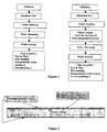
The active face is generally already coated with a passivation layer in order to better protect the active face. A passivation layer generally comprises Si02 or Si3N4. Other well known material can be used. - As illustrated in figure 1, standard smart card manufacturing process uses "naked" chip for microelectronic packaging, with process described as below:
- Wafer foundry, diffusion and testing.
- Wafer thinning.
- Wafer mounting.
- Wafer sawing.
- Chip pick & place on lead-frame or other package type.
- Wire bonding
- Resin coating or over moulding.
- It is an object of the invention to enhance the quality and to reduce the costs.
- According to one aspect of the invention, a slice of semiconductor comprises an active face and an inactive face, a passivation layer being deposited on the active face, wherein the inactive face is provided with an organic layer.
- The slice of semiconductor is, for example, a silicon wafer. The organic layer can be, for example, a polyimide, a thermic curing resin (epoxy basis), UV curing resin, an adhesive ("scotch") or a glue.
The organic-layer-depositing step can be introduced, for example, between the wafer-thinning step and the wafer-mounting step.
Silicon is a very brittle material, especially for thin chip application. During most of the above-mentioned manufacturing steps, the silicon is made fragile due to mechanical constraints faced, so chip breakage risk is very high. In order to increase chip reliability, chipping and crack on chip (or wafer) edges must be minimised, and the chip must be reinforced too.
By providing the inactive face of the wafer with an organic layer, a composite structure (organic/mineral/organic) is obtained. Therefore the mechanical stress induced by the passivation layer on the active face is reduced. The organic layer compensates the initial wafer stress. Thus the wafer bow and warping is reduced. The flatness of the wafer is therefore improved.
By providing the inactive face with an organic layer, chipping and crack propagation into silicon during wafer mounting, wafer sawing and pick & place steps is also reduced. The thus obtained chips have a composite structure (organic / mineral / organic) so that they are more rigid. Then, due to this global mechanical behaviour improvement, the lifetime of the final product, for example, a smart card, is significantly increased. During, for example, the "3wheels" test as defined in the ISO standards 7810 and 10373.1, the stress applied on the chip is reduced by 9%.
According to another advantage of the invention, the organic layer is made of an organic material. Thus the depositing step can be done using just a spin coating process, which is easy to implement and cost effective.
Thus the invention allows a reduction of the cost and an enhanced quality. - According to another aspect of the invention, a second organic layer can be deposited on the passivation layer of the wafer so that the wafer bow and warping are more reduced. Advantageously the second organic layer is made of a photo sensitive resin using, for example, a photo-lithographic process (photo sensitive resin coating by liquid spinning, curing, exposure, development, etc...). Using a photo sensitive material enables to create opening within the second organic above the contact pads of the active surface.
- According to another aspect of the invention, the second organic layer can be deposited of on a shielding layer which has been placed on the active face of the wafer. Advantageously the shielding layer is made of the same material than the wafer. Advantageously, the shielding layer is provider with holes being located flush with at least one integrated circuit element of the active face of the wafer.
- The description hereinbefore illustrates a slice of semiconductor comprising an active face and an inactive face. A passivation layer is deposited on the active face. The inactive face is provided with an organic layer.
- The slice of semiconductor is, for example, made of silicon. It can be, in particular a silicon wafer.
- The organic layer can be any organic layer than can be deposited on a slice of silicon, for example, a polyimide, a thermic curing resin (epoxy basis), UV curing resin, an adhesive ("scotch") or a glue.
Note that the invention also applies in the case where there is no passivation layer. In this case it is necessary to deposit the second organic layer on the active face so as to obtain a composite structure (organic/mineral/organic). The mechanical stress due to the first organic layer thus compensates the mechanical stress due to the second organic layer.
Claims (4)
- A slice of semiconductor comprising an active face and an inactive face, a passivation layer being deposited on the active face, wherein the inactive face is provided with an organic layer.
- The slice of semiconductor according to claim 1, wherein the passivation layer is provided with a second organic layer.
- The slice of semiconductor according to claim 1, wherein the organic layer is a polyimide.
- The slice of semiconductor according to claim 2, wherein the second organic layer is made of a photosensitive resin.
Priority Applications (6)
| Application Number | Priority Date | Filing Date | Title |
|---|---|---|---|
| EP03077862A EP1447844A3 (en) | 2003-02-11 | 2003-08-28 | Reinforced semiconductor wafer |
| JP2006502421A JP2006517736A (en) | 2003-02-11 | 2004-02-10 | Method for manufacturing an enhanced semiconductor wafer |
| US10/545,357 US20060134887A1 (en) | 2003-02-11 | 2004-02-10 | Method of manufacturing a slice of semiconductor |
| KR1020057014694A KR20050101329A (en) | 2003-02-11 | 2004-02-10 | Method of manufacturing a reinforced semiconductor wafer |
| PCT/IB2004/000335 WO2004073062A2 (en) | 2003-02-11 | 2004-02-10 | Method of manufacturing a reinforced semiconductor wafer |
| EP04709668A EP1593156A2 (en) | 2003-02-11 | 2004-02-10 | Method of manufacturing a slice of semiconductor |
Applications Claiming Priority (3)
| Application Number | Priority Date | Filing Date | Title |
|---|---|---|---|
| EP03290336 | 2003-02-11 | ||
| EP03290336 | 2003-02-11 | ||
| EP03077862A EP1447844A3 (en) | 2003-02-11 | 2003-08-28 | Reinforced semiconductor wafer |
Publications (2)
| Publication Number | Publication Date |
|---|---|
| EP1447844A2 true EP1447844A2 (en) | 2004-08-18 |
| EP1447844A3 EP1447844A3 (en) | 2004-10-06 |
Family
ID=32683843
Family Applications (2)
| Application Number | Title | Priority Date | Filing Date |
|---|---|---|---|
| EP03077862A Withdrawn EP1447844A3 (en) | 2003-02-11 | 2003-08-28 | Reinforced semiconductor wafer |
| EP04709668A Withdrawn EP1593156A2 (en) | 2003-02-11 | 2004-02-10 | Method of manufacturing a slice of semiconductor |
Family Applications After (1)
| Application Number | Title | Priority Date | Filing Date |
|---|---|---|---|
| EP04709668A Withdrawn EP1593156A2 (en) | 2003-02-11 | 2004-02-10 | Method of manufacturing a slice of semiconductor |
Country Status (5)
| Country | Link |
|---|---|
| US (1) | US20060134887A1 (en) |
| EP (2) | EP1447844A3 (en) |
| JP (1) | JP2006517736A (en) |
| KR (1) | KR20050101329A (en) |
| WO (1) | WO2004073062A2 (en) |
Family Cites Families (25)
| Publication number | Priority date | Publication date | Assignee | Title |
|---|---|---|---|---|
| DE2929339A1 (en) * | 1978-07-24 | 1980-02-14 | Citizen Watch Co Ltd | SEMICONDUCTOR ARRANGEMENT |
| JPS5518069A (en) * | 1978-07-26 | 1980-02-07 | Citizen Watch Co Ltd | Protective construction of semiconductor device |
| JP3376203B2 (en) * | 1996-02-28 | 2003-02-10 | 株式会社東芝 | Semiconductor device, method of manufacturing the same, mounting structure using the semiconductor device, and method of manufacturing the same |
| US6441487B2 (en) * | 1997-10-20 | 2002-08-27 | Flip Chip Technologies, L.L.C. | Chip scale package using large ductile solder balls |
| US6023094A (en) * | 1998-01-14 | 2000-02-08 | National Semiconductor Corporation | Semiconductor wafer having a bottom surface protective coating |
| US6075290A (en) * | 1998-02-26 | 2000-06-13 | National Semiconductor Corporation | Surface mount die: wafer level chip-scale package and process for making the same |
| JP3441382B2 (en) * | 1998-10-14 | 2003-09-02 | 日本電信電話株式会社 | Method for manufacturing semiconductor device |
| CN1190837C (en) * | 1999-02-15 | 2005-02-23 | 株式会社日立制作所 | Semiconductor device, method of manufacture thereof, electronic device |
| US6323060B1 (en) * | 1999-05-05 | 2001-11-27 | Dense-Pac Microsystems, Inc. | Stackable flex circuit IC package and method of making same |
| US6579748B1 (en) * | 1999-05-18 | 2003-06-17 | Sanyu Rec Co., Ltd. | Fabrication method of an electronic component |
| JP2001094005A (en) * | 1999-09-22 | 2001-04-06 | Oki Electric Ind Co Ltd | Semiconductor device and method of manufacturing semiconductor device |
| JP3604988B2 (en) * | 2000-02-14 | 2004-12-22 | シャープ株式会社 | Semiconductor device and manufacturing method thereof |
| FR2806189B1 (en) * | 2000-03-10 | 2002-05-31 | Schlumberger Systems & Service | REINFORCED INTEGRATED CIRCUIT AND METHOD FOR REINFORCING INTEGRATED CIRCUITS |
| JP3631956B2 (en) * | 2000-05-12 | 2005-03-23 | 富士通株式会社 | Semiconductor chip mounting method |
| US6603191B2 (en) * | 2000-05-18 | 2003-08-05 | Casio Computer Co., Ltd. | Semiconductor device and method of manufacturing the same |
| US6326698B1 (en) * | 2000-06-08 | 2001-12-04 | Micron Technology, Inc. | Semiconductor devices having protective layers thereon through which contact pads are exposed and stereolithographic methods of fabricating such semiconductor devices |
| TW522531B (en) * | 2000-10-20 | 2003-03-01 | Matsushita Electric Industrial Co Ltd | Semiconductor device, method of manufacturing the device and mehtod of mounting the device |
| JP2002353369A (en) * | 2001-05-28 | 2002-12-06 | Sharp Corp | Semiconductor package and manufacturing method thereof |
| US20030017626A1 (en) * | 2001-07-23 | 2003-01-23 | Motorola Inc. | Method and apparatus for controlling propagation of dislocations in semiconductor structures and devices |
| US7169685B2 (en) * | 2002-02-25 | 2007-01-30 | Micron Technology, Inc. | Wafer back side coating to balance stress from passivation layer on front of wafer and be used as die attach adhesive |
| US6908784B1 (en) * | 2002-03-06 | 2005-06-21 | Micron Technology, Inc. | Method for fabricating encapsulated semiconductor components |
| JP3595323B2 (en) * | 2002-11-22 | 2004-12-02 | 沖電気工業株式会社 | Semiconductor device and manufacturing method thereof |
| JP4660259B2 (en) * | 2004-06-10 | 2011-03-30 | 三洋電機株式会社 | Manufacturing method of semiconductor device |
| JP4165467B2 (en) * | 2004-07-12 | 2008-10-15 | セイコーエプソン株式会社 | Dicing sheet and method for manufacturing semiconductor device |
| US7232770B2 (en) * | 2005-05-03 | 2007-06-19 | General Chemical Performance Products Llc | High temperature and chemical resistant process for wafer thinning and backside processing |
-
2003
- 2003-08-28 EP EP03077862A patent/EP1447844A3/en not_active Withdrawn
-
2004
- 2004-02-10 EP EP04709668A patent/EP1593156A2/en not_active Withdrawn
- 2004-02-10 JP JP2006502421A patent/JP2006517736A/en active Pending
- 2004-02-10 US US10/545,357 patent/US20060134887A1/en not_active Abandoned
- 2004-02-10 WO PCT/IB2004/000335 patent/WO2004073062A2/en not_active Ceased
- 2004-02-10 KR KR1020057014694A patent/KR20050101329A/en not_active Withdrawn
Non-Patent Citations (1)
| Title |
|---|
| None * |
Also Published As
| Publication number | Publication date |
|---|---|
| WO2004073062A2 (en) | 2004-08-26 |
| EP1447844A3 (en) | 2004-10-06 |
| KR20050101329A (en) | 2005-10-21 |
| EP1593156A2 (en) | 2005-11-09 |
| JP2006517736A (en) | 2006-07-27 |
| WO2004073062A3 (en) | 2004-10-21 |
| US20060134887A1 (en) | 2006-06-22 |
Similar Documents
| Publication | Publication Date | Title |
|---|---|---|
| JP3456462B2 (en) | Semiconductor device and manufacturing method thereof | |
| US6023094A (en) | Semiconductor wafer having a bottom surface protective coating | |
| KR100517075B1 (en) | Method for manufacturing semiconductor device | |
| US20050095750A1 (en) | Wafer level transparent packaging | |
| US7705468B2 (en) | Stacked semiconductor package that prevents damage to semiconductor chip when wire-bonding and method for manufacturing the same | |
| US20120104454A1 (en) | Optical device, process for fabricating it and an electronic package comprising this optical device | |
| US20230130127A1 (en) | Method for manufacturing a functional chip suitable for being assembled to wire elements | |
| US20080014719A1 (en) | Semiconductor device and manufacturing method for the same | |
| US20130119538A1 (en) | Wafer level chip size package | |
| US20090026593A1 (en) | Thin semiconductor die packages and associated systems and methods | |
| US20120001328A1 (en) | Chip-sized package and fabrication method thereof | |
| US8779573B2 (en) | Semiconductor package having a silicon reinforcing member embedded in resin | |
| US20090239329A1 (en) | Method for manufacturing package structure of optical device | |
| US20070155049A1 (en) | Method for Manufacturing Chip Package Structures | |
| US20060270104A1 (en) | Method for attaching dice to a package and arrangement of dice in a package | |
| KR20120012404A (en) | Method for Forming Cap-type Micro-electro-mechanical System Devices | |
| US7256108B2 (en) | Method for reducing semiconductor die warpage | |
| US20020014693A1 (en) | Molded array package for facilitating device singulation | |
| US20080029865A1 (en) | Electronic Device and Method For Producing the Same | |
| KR100927778B1 (en) | Semiconductor Package Manufacturing Method | |
| US20060134887A1 (en) | Method of manufacturing a slice of semiconductor | |
| JP4107896B2 (en) | Semiconductor device and manufacturing method thereof | |
| CN101211791B (en) | Wafer level chip packaging process and chip packaging structure | |
| US20120061830A1 (en) | Back side protective structure for a semiconductor package | |
| US7696008B2 (en) | Wafer-level chip packaging process and chip package structure |
Legal Events
| Date | Code | Title | Description |
|---|---|---|---|
| PUAI | Public reference made under article 153(3) epc to a published international application that has entered the european phase |
Free format text: ORIGINAL CODE: 0009012 |
|
| AK | Designated contracting states |
Kind code of ref document: A2 Designated state(s): AT BE BG CH CY CZ DE DK EE ES FI FR GB GR HU IE IT LI LU MC NL PT RO SE SI SK TR |
|
| AX | Request for extension of the european patent |
Extension state: AL LT LV MK |
|
| PUAL | Search report despatched |
Free format text: ORIGINAL CODE: 0009013 |
|
| RAP1 | Party data changed (applicant data changed or rights of an application transferred) |
Owner name: AXALTO S.A. |
|
| AK | Designated contracting states |
Kind code of ref document: A3 Designated state(s): AT BE BG CH CY CZ DE DK EE ES FI FR GB GR HU IE IT LI LU MC NL PT RO SE SI SK TR |
|
| AX | Request for extension of the european patent |
Extension state: AL LT LV MK |
|
| RIC1 | Information provided on ipc code assigned before grant |
Ipc: 7H 01L 21/56 B Ipc: 7H 01L 23/00 B Ipc: 7H 01L 23/31 A |
|
| AKX | Designation fees paid | ||
| REG | Reference to a national code |
Ref country code: DE Ref legal event code: 8566 |
|
| 17P | Request for examination filed |
Effective date: 20050527 |
|
| RBV | Designated contracting states (corrected) |
Designated state(s): AT BE BG CH CY CZ DE DK EE ES FI FR GB GR HU IE IT LI LU MC NL PT RO SE SI SK TR |
|
| 17Q | First examination report despatched |
Effective date: 20061204 |
|
| STAA | Information on the status of an ep patent application or granted ep patent |
Free format text: STATUS: THE APPLICATION IS DEEMED TO BE WITHDRAWN |
|
| 18D | Application deemed to be withdrawn |
Effective date: 20070417 |