EP1447811A1 - Ferroelectric storage device, drive method and drive circuit thereof - Google Patents
Ferroelectric storage device, drive method and drive circuit thereof Download PDFInfo
- Publication number
- EP1447811A1 EP1447811A1 EP03745016A EP03745016A EP1447811A1 EP 1447811 A1 EP1447811 A1 EP 1447811A1 EP 03745016 A EP03745016 A EP 03745016A EP 03745016 A EP03745016 A EP 03745016A EP 1447811 A1 EP1447811 A1 EP 1447811A1
- Authority
- EP
- European Patent Office
- Prior art keywords
- bit
- word
- line driver
- ferroelectric
- selection
- Prior art date
- Legal status (The legal status is an assumption and is not a legal conclusion. Google has not performed a legal analysis and makes no representation as to the accuracy of the status listed.)
- Granted
Links
Images









Classifications
-
- G—PHYSICS
- G11—INFORMATION STORAGE
- G11C—STATIC STORES
- G11C11/00—Digital stores characterised by the use of particular electric or magnetic storage elements; Storage elements therefor
- G11C11/21—Digital stores characterised by the use of particular electric or magnetic storage elements; Storage elements therefor using electric elements
- G11C11/22—Digital stores characterised by the use of particular electric or magnetic storage elements; Storage elements therefor using electric elements using ferroelectric elements
Definitions
- the present invention relates to ferroelectric storage apparatuses, driving methods therefor, and driving circuits therefor.
- Ferroelectric storage apparatuses having ferroelectric capacitors as storage elements are expected to serve as memory devices which have a possibility of substituting for conventional memories because the ferroelectric storage apparatuses have an operation speed as fast as DRAMs and are non-volatile as flash memories.
- active ferroelectric memories which have 1T/1C cells each of which has one transistor and one capacitor (ferroelectric) or 2T/2C cells each of which has a 1T/1C cell and a reference cell. Since there is a limit on the level of integration of 1T/1C cells and 2T/2C cells, a smaller memory-element structure is demanded in terms of future high integration.
- the 1C-cell structure Since an unnecessary voltage is applied during a non-selection period in the 1C-cell structure, however, the data may deteriorate to cause disturbance finally in which the storage state cannot be determined. Therefore, the 1C-cell structure has not yet been made practical.
- An object of the present invention is to provide ferroelectric storage apparatuses which can prevent the disturbance, driving methods therefor, and driving circuits therefor.
- an operation step (operation mode) of applying one of data reading, data re-writing, and data writing to at least one selected cell among a plurality of ferroelectric memory cells formed at the intersections of a plurality of word lines and a plurality of bit lines is performed.
- a disturbance prevention step (disturbance prevention mode) of applying a voltage to each of the plurality of ferroelectric memory cells in an electric-field direction in which the stored data of each ferroelectric memory cell is not inverted is performed after the operation step is executed at least once.
- the present invention is especially suited to so-called crossing-point or passive ferroelectric storage apparatuses in which each of the plurality of ferroelectric memory cells is formed of a ferroelectric capacitor only. This is because, in this case, although a voltage may be applied to the not-selected cells in an electric-field direction in which the stored data of the not-selected cells is inverted, when the operation step is applied to the selected cell, the disturbance prevention step prevents a voltage from being continuously applied to the not-selected cells in the electric-field direction in which the stored data of the non-selected cells is inverted.
- one of a first-polarity selection voltage or a second-polarity selection voltage is applied to the at least one selected cell, and one or both of a first-polarity non-selection voltage and a second-polarity non-selection voltage is applied to not-selected cells.
- the first-polarity non-selection voltage and the second-polarity non-selection voltage may be alternately applied to each of the plurality of ferroelectric memory cells.
- a ferroelectric storage apparatus has a structure which includes a plurality of word lines disposed in parallel to each other; a plurality of bit lines disposed in parallel to each other and intersecting with the plurality of word lines; a plurality of ferroelectric memory cells formed at the intersections of the plurality of word lines and the plurality of bit lines; a word-line driver for driving the plurality of word lines; and a bit-line driver for driving the plurality of bit lines.
- the word-line driver and the bit-line driver of the above-described ferroelectric storage apparatus are disposed. The method described above according to the present invention is performed also in the ferroelectric storage apparatuses and the driving circuit.
- Fig. 1 is a block diagram of an FeRAM serving as a ferroelectric storage apparatus according to a first embodiment of the present invention
- Fig. 2 is a perspective view showing a memory array thereof in a sketch manner.
- a memory cell array 10 includes a ferroelectric thin film 12, a plurality of word lines 14 arranged on one surface of the ferroelectric thin film 12, and a plurality of bit lines 16 arranged on the other surface of the ferroelectric thin film 12.
- a ferroelectric memory cell 18 is formed as shown in Fig. 1.
- the memory shown in Fig. 2 is called a crossing-point FeRAM or a passive FeRAM. Therefore, the memory shown in Fig. 2 is different from an active memory, which has 1T/1C cells each of which has one transistor and one capacitor (ferroelectric) or 2T/2C cells each of which has a 1T/1C cell and a reference cell.
- the FeRAM according to the present invention does not need to have transistors in the memory cell array 10, it can be highly integrated, and in addition, the structure shown in Fig. 2 can be laminated in multiple stages.
- a driving circuit substrate on which a CMOS logic is mounted can be disposed, for example, below the structure shown in Fig. 2.
- an inorganic material such as SBT (strontium-bismuth-tantalum), PZT (lead-zirconium-titanium), BLT (bismuth-lanthanum-titanium) or an oxide of one of these, can be suitably used.
- SBT Strontium-bismuth-tantalum
- PZT lead-zirconium-titanium
- BLT bismuth-lanthanum-titanium
- Other inorganic materials, or organic materials may be used.
- platinum Pt
- iridium Ir
- iridium oxide IrO2
- strontium-ruthenium or an oxide of one of these can be suitably used in view of their high oxidation resistance and heat resistance.
- Other electrically conductive material may be used.
- a word-line driver 20 for driving the plurality of word lines 14, a bit-line driver 22 for driving the plurality of bit lines 16, and a power-supply circuit 24 for supplying a plurality of types of driving voltages (Vs, 2Vs/3, Vs/3, and 0) to the word-line driver 10 and the bit-line driver 22 are provided.
- the word-line driver 20 is connected to an end (lefthand end in Fig. 1) of each of the plurality of word lines 14, and the bit-line driver 22 is connected to one end (upper-end in Fig. 1) of each of the plurality of bit lines 16.
- the word-line driver 20 includes a row-direction address decoder, and supplies the potential corresponding to a read mode, a write mode, or a rewrite mode (and data to be written in the write mode or the rewrite mode) to one word line 14 address selected, and to the other not-selected word lines 14.
- the bit-line driver 22 includes a column-direction address decoder, and supplies the potential corresponding to the read mode, the write mode, or the rewrite mode (and data to be written in the write mode or the rewrite mode) to at least one bit line 16 address selected, and to the other not-selected bit lines 14.
- the word-line driver 20 and the bit-line driver 22 supply the potential to the word lines 14 and the bit lines 16 in the above-described operation modes, and in addition, have a function to supply a potential to the word lines 14 and the bit lines 16 in order to perform a disturbance prevention step thereafter.
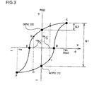
- Fig. 3 shows the hysteresis characteristic of the voltage dependency of spontaneous polarization P or a polarization charge Q (a change in polarization multiplied by the area of the capacitor) in the memory cell 18 shown in Fig. 1.
- a direction in which the potential of the word lines 14 becomes higher than that of the bit lines 16 is set to a plus direction as an example.
- the voltage applied to the memory cell 18 is 0 V.
- the ferroelectric capacitor has two types of residual dielectric polarization ⁇ Pr (points A and D in Fig. 3).
- Points C and F in Fig. 3 indicate the saturated polarization points of the ferroelectric memory cell 18.
- the polarization direction reverses at points B and E in Fig. 3.
- voltages which make the polarization value zero are called coercive voltages.
- Data is read by applying a voltage +Vs to the ferroelectric memory cell 18 which is in the polarization state at point A or at point D.
- Potential settings for the word lines 14 and the bit lines 16 will be described next by taking reading of data as an example. These potential settings are performed by the word-line driver 20 and the bit-line driver 22, which receive the four types of potentials (Vs, 2Vs/3, Vs/3, and 0) from the power-supply circuit 24. Potentials of Vs and 0 serve as two types of selection potentials, and potentials of 2Vs/3 and Vs/3 serve as two types of non-selection potentials.
- Fig. 4 shows one selected cell 18a and other not-selected cells 18b.
- Vs word selection potential
- An actual data read operation is applied to a plurality of memory cells 18 connected to one word line 14 at the same time, and a group of data, such as eight-bit data or 16-bit data, is read at a time.
- all the word lines 14 connected to the not-selected cells 18b shown in Fig. 4 are set to have a potential of Vs/3 (word non-selection potential), and all the bit lines 16 connected to the not-selected cells 18b are set to have a potential of 2Vs/3 (bit non-selection potential).
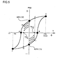
- Fig. 5 shows a case in which a non-selection voltage of -Vs/3 is applied 10 n -order times repeatedly at every operation mode of a selected cell, in the electric-field direction in which the polarization state is inverted (the electric-field direction used in transition toward point E, which is the negative electric-field direction) to not-selected memory cells which are at the polarization state of point D.
- Fig. 5 shows a case in which a non-selection voltage of -Vs/3 is applied 10 n -order times repeatedly at every operation mode of a selected cell, in the electric-field direction in which the polarization state is inverted (the electric-field direction used in transition toward point E, which is the negative electric-field direction) to not-selected memory cells which are at the polarization state of point D.
- FIG. 5 shows a case in which a non-selection voltage of Vs/3 is applied 10 n -order times repeatedly at every operation mode of a selected cell, in electric-field directions in which the polarization state is inverted (the electric-field direction used in transition toward point B, which is the positive electric-field direction) to not-selected memory cells which are at the polarization state of point A.
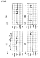
- Fig. 6(A) shows a driving method in a comparison example
- Fig. 6(B) shows a driving method in the present embodiment.
- Both Fig. 6(A) and Fig. 6(B) show a case in which a writing pulse (-Vs) in the negative electric-field direction is applied to a ferroelectric capacitor to make a transition of the polarization state to point F in Fig. 3, and data "1" is written.
- This writing operation is the same as a re-writing operation used for making a transition to point F through point D in Fig. 3 after a transition is made from point A (a state where data "1" is stored) in Fig. 3 to point C to read data "1".
- a non-selection voltage (Vs/3) in the positive electric-field direction is repeatedly applied, and then, a reading pulse in the positive electric-field direction is applied to perform reading.
- Vs/3 a non-selection voltage
- a reading pulse in the positive electric-field direction is applied to perform reading.
- This operation will be described by referring to Fig. 5.
- Data "1" is written, and a transition is made to the polarization state of point F.
- a voltage of 0 is applied, and the memory state is in the polarization state of point A in Fig. 5.
- a non-selection voltage of Vs/3 is repeatedly applied to cause the disturbance phenomenon as shown in Fig. 5. Therefore, the amount of polarization charges obtained when a reading pulse Vs in the positive electric-field direction is applied is smaller than the amount Q1 of polarization charges shown in Fig. 3, obtained when the disturbance phenomenon does not occur.
- a pair of non-selection pulses (-Vs/3 and +Vs/3) is always applied during repeatedly generated non-selection periods. Therefore, in the case shown in Fig. 6(B), since the negative-electric-field non-selection pulse (-Vs/3) serves as a voltage pulse in the electric-field direction in which the polarization state of point A in Fig. 5 is not inverted, the disturbance phenomenon is suppressed similarly.
- the present embodiment is not necessarily limited to a case in which a pair of non-selection pulses is applied.
- a method in which a non-selection pulse in the positive electric-field direction and a non-selection pulse in the negative electric-field direction are alternately applied at a predetermined frequency can be employed.
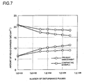
- Fig. 7 is a characteristic view showing the relationship between the number of times non-selection pulses are applied and the amount of read charges for each of the comparison example shown in Fig. 6(A) and the present embodiment shown in Fig. 6(B). As clearly shown in Fig. 7, it is understood that, in the present embodiment, a less adverse effect of the disturbance phenomenon is given, and a larger amount of read charges is obtained.
- a cell C11 shown in Fig. 8 is a selected cell, and cells C12, C21, and C22 are cells not selected.
- Fig. 9(A) to Fig. 9(D) show the potentials of two word lines WL1 and WL2 and the potentials of two bit lines BL1 and BL2, obtained when data "0" is written into the selected cell C11, as shown in Fig. 3, or data "0" and data "1” is read, as shown in Fig. 3.
- Fig. 10(A) to Fig. 10(D) show the voltages applied to the four cells C11, C12, C21, and C22 when the potentials shown in Fig. 9(A) to Fig. 9(D) are applied to the word lines WL1 and WL2 and the bit lines BL1 and BL2.
- a driving period shown in each of the figures is divided into a data "1" writing period T1, an equalization period T2, and a disturbance prevention period T3.
- the writing period T1 5W
- the equalization period T2 W
- the disturbance prevention period T3 3W, where W indicates the minimum pulse width.
- a word non-selection potential (Vs/3) is applied to the word line WL2 as shown in Fig. 9(B), and a bit-line non-selection potential (2Vs/3) is applied to the bit line BL2 as shown in Fig. 9(D).
- the non-selection word potential (Vs/3) having a pulse width of 3W is applied to the bit line BL2
- the non-selection word potential (Vs/3) having a pulse width of 5W is applied to the word lines WL1 and L2.
- the potentials of all the word lines and bit lines are set to 0 V.
- the polarization state of the selected cell is changed such that a transition is made to point C in Fig. 3 at the previous writing period T1, a transition is made to point J within the writing period T1, and a transition is made to point D by an equalization operation.
- a transition is made to either point G or point J (when the state was at point D) or to either point H or point I (when the state was at point A), and then, a transition is made to the original point D or A.
- the disturbance prevention period T3 is divided into three zones, a first zone T 31 and a second zone T 32 where the non-selection potential (Vs/3) is applied, and a third zone T 33 where the lines are set to 0 V therebetween.
- the non-selection potential (Vs/3) is applied to all the word lines WL1 and WL2.
- the non-selection potential (Vs/3) is applied to all the bit lines BL1 and BL2.
- the first zone and the second zone may be switched in their order.
- the third zone T 33 is the same as the equalization period T2, described above.
- the positive-electric-field non-selection potential (Vs/3) is applied in the first zone T31, and the negative-electric-field non-selection voltage (-Vs/3) is applied in the second zone T32, to all the cells C11, C12, C21, and C22. Therefore, according to the principle described by referring to Fig. 6(B), disturbance is prevented.
- the non-selection voltages ( ⁇ Vs/3) in both electric-field directions are applied to the not-selected cells C12 and C22 shown in Fig. 10(B) and Fig. 10(D) during the writing period T1, but the non-selection voltage in one electric-field direction is continuously applied to the not-selected cell C21 shown in Fig. 10(C) during the writing period T1. Therefore, depending on the memory state of the not-selected cell C21, the most severe adverse effect of disturbance occurs. Even in this case, by providing the disturbance period T3 according to the present embodiment, since a non-selection voltage in the electric-field direction in which the memory state is not inverted is always applied periodically, the disturbance problem is suppressed.
- Fig. 11(A) to Fig. 11(D) show the potentials of the two word lines WL1 and WL2 and the potentials of the two bit lines BL1 and BL2, obtained when data "1" is written into the selected cell C11, as shown in Fig. 3.
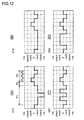
- Fig. 12(A) to Fig. 12(D) show the voltages applied to the four cells C11, C12, C21, and C22 when the potentials shown in Fig. 11(A) to Fig. 11(D) are applied to the word lines WL1 and WL2 and the bit lines BL1 and BL2.
- the disturbance prevention period is provided every time a writing operation, a re-writing operation, and a reading operation are finished.
- the disturbance period may be provided every time a plurality of these operations is finished.
- a counter 40 can be provided, which counts the number of times a writing operation or a reading operation is performed, and which instructs to start the operation of the disturbance prevention period T3 when the count reaches a predetermined value.
- the counter 40 may count, for example, an address transition signal ATD to count the number of times a writing operation or a reading operation is performed. It is necessary to always perform a re-writing operation immediately after a reading operation, and to perform writing twice, namely, to write data "0" and data "1" in a writing operation. Therefore, when the counter 40 counts the address transition signal ATD once, it means that the above-described two operations are finished. With this taken into account, the count needs to be determined.
- Fig. 14 shows another embodiment in which the operation of the disturbance prevention period T3 is performed when a dummy address (M+1, N+1) which is not used as a memory address is specified.
- Fig. 14 there are N effective word lines 14, M effective bit lines 16, and a total of M-by-N ferroelectric memory cells 18.
- the (N+1)-th imaginary word line 14A and the (M+1)-th imaginary bit line 16A are assumed.
- the address (M+1, N+1) is also an imaginary address.
- the word-line driver 20 and the bit-line driver 22 are set such that when an imaginary address, for example, the address (M, N) is specified, the disturbance prevention step is performed. With this, the disturbance prevention step can be executed just by specifying an address, without using the counter 40 and others.
Landscapes
- Engineering & Computer Science (AREA)
- Computer Hardware Design (AREA)
- Semiconductor Memories (AREA)
- Dram (AREA)
- Soundproofing, Sound Blocking, And Sound Damping (AREA)
- Electrotherapy Devices (AREA)
- Valve Device For Special Equipments (AREA)
Abstract
Description
Claims (11)
- A driving method for a ferroelectric storage apparatus, characterized by comprising:an operation step of applying one of data reading, data re-writing, and data writing to at least one selected cell among a plurality of ferroelectric memory cells formed at the intersections of a plurality of word lines and a plurality of bit lines; and a disturbance prevention step of applying a voltage to each of the plurality of ferroelectric memory cells in an electric-field direction in which the stored data of each ferroelectric memory cell is not inverted, after the operation step is executed at least once.
- A driving method for a ferroelectric storage apparatus, according to Claim 1,
characterized in that each of the plurality of ferroelectric memory cells is formed of a ferroelectric capacitor only. - A driving method for a ferroelectric storage apparatus, according to Claim 1 or 2,
characterized in that, in the operation step, one of a first-polarity selection voltage and a second-polarity selection voltage is applied to the at least one selected cell, and one or both of a first-polarity non-selection voltage and a second-polarity non-selection voltage is applied to not-selected cells; and
in the disturbance prevention step, the first-polarity non-selection voltage and the second-polarity non-selection voltage are alternately applied to each of the plurality of ferroelectric memory cells. - A ferroelectric storage apparatus characterized by comprising:characterized in that the word-line driver and the bit-line driver apply an operation mode of one of data reading, data re-writing, and data writing to at least one selected cell among the plurality of ferroelectric memory cells, and apply a voltage to each of the plurality of ferroelectric memory cells in an electric-field direction in which the stored data of each ferroelectric memory cell is not inverted, during a disturbance prevention mode performed after the operation mode is performed at least once.a plurality of word lines disposed in parallel to each other;a plurality of bit lines disposed in parallel to each other and intersecting with the plurality of word lines;a plurality of ferroelectric memory cells formed at the intersections of the plurality of word lines and the plurality of bit lines;a word-line driver for driving the plurality of word lines; anda bit-line driver for driving the plurality of bit lines, and
- A ferroelectric storage apparatus according to Claim 4,
characterized in that each of the plurality of ferroelectric memory cells is formed of a ferroelectric capacitor only. - A ferroelectric storage apparatus according to Claim 4 or 5,
characterized in that the word-line driver and the bit-line driver apply, in the operation mode, one of the first-polarity selection voltage and the second-polarity selection voltage to the at least one selected cell, and apply one or both of a first-polarity non-selection voltage and a second-polarity non-selection voltage to not-selected cells; and
in the disturbance prevention mode, apply the first-polarity non-selection voltage and the second-polarity non-selection voltage alternately to each of the plurality of ferroelectric memory cells. - A ferroelectric storage apparatus according to Claim 6,
characterized in that, in the operation mode, the word-line driver supplies one of two types of selection potentials to a word line connected to the at least one selected cell, and supplies one of two types of non-selection potentials to word lines connected to the not-selected cells, and the bit-line driver supplies the other of the two types of selection potentials to a bit line connected to the at least one selected cell, and supplies the other of the two types of non-selection potential to bit lines connected to the not-selected cells; and
the disturbance prevention mode is divided into a first zone and a second zone; in the first zone, the word-line driver supplies one of the two types of non-selection potentials to the plurality of word lines, and the bit-line driver supplies the other of the two types of non-selection potentials to the plurality of bit lines; and in the second zone, the word-line driver supplies the other of the two types of non-selection potentials to the plurality of word lines, and the bit-line driver supplies the one of the two types of non-selection potentials to the plurality of bit lines. - A ferroelectric storage apparatus according to Claim 7,
characterized in that the word-line driver and the bit-line driver set the plurality of word lines and the plurality of bit lines to the same potential during a third zone provided between the first zone and the second zone. - A ferroelectric storage apparatus according to one of Claims 5 to 8,
characterized by further comprising a counter for counting the number of times the operation mode is performed, and characterized in that the word-line driver and the bit-line driver perform the disturbance prevention mode according to the output of the counter. - A ferroelectric storage apparatus according to one of Claims 5 to 8,
characterized in that the word-line driver is connected to N word lines, the bit-line driver is connected to M bit lines, a total of N-by-M ferroelectric memory cells are disposed, and the word-line driver and the bit-line driver perform the operation mode when at least one effective address in the N-by-M ferroelectric memory cells is selected, and perform the disturbance prevention mode when a dummy address other than the effective address is selected. - A driving circuit connected to a ferroelectric storage section provided with a plurality of ferroelectric memory cells formed at the intersections of a plurality of word lines and a plurality of bit lines, characterized by comprising:characterized in that the word-line driver and the bit-line drivers apply an operation mode of one of data reading, data re-writing, and data writing to at least one selected cell among the plurality of ferroelectric memory cells, formed at the intersections of the plurality of word lines and the plurality of bit lines, and apply a voltage to each of the plurality of ferroelectric memory cells in an electric-field direction in which the stored data of each ferroelectric memory cell is not inverted, during a disturbance prevention mode performed after the operation mode is performed at least once.a word-line driver for driving the plurality of word lines; anda plurality of bit-line drivers for driving the plurality of bit lines, and
Applications Claiming Priority (3)
| Application Number | Priority Date | Filing Date | Title |
|---|---|---|---|
| JP2002089173 | 2002-03-27 | ||
| JP2002089173A JP4214708B2 (en) | 2002-03-27 | 2002-03-27 | Ferroelectric memory device and driving method thereof |
| PCT/JP2003/003909 WO2003081601A1 (en) | 2002-03-27 | 2003-03-27 | Ferroelectric storage device, drive method and drive circuit thereof |
Publications (3)
| Publication Number | Publication Date |
|---|---|
| EP1447811A1 true EP1447811A1 (en) | 2004-08-18 |
| EP1447811A4 EP1447811A4 (en) | 2006-06-07 |
| EP1447811B1 EP1447811B1 (en) | 2009-03-11 |
Family
ID=28449493
Family Applications (1)
| Application Number | Title | Priority Date | Filing Date |
|---|---|---|---|
| EP03745016A Expired - Lifetime EP1447811B1 (en) | 2002-03-27 | 2003-03-27 | Ferroelectric storage device, drive method and drive circuit thereof |
Country Status (8)
| Country | Link |
|---|---|
| US (1) | US6788564B2 (en) |
| EP (1) | EP1447811B1 (en) |
| JP (1) | JP4214708B2 (en) |
| KR (1) | KR100589732B1 (en) |
| CN (1) | CN100405501C (en) |
| AT (1) | ATE425538T1 (en) |
| DE (1) | DE60326535D1 (en) |
| WO (1) | WO2003081601A1 (en) |
Families Citing this family (16)
| Publication number | Priority date | Publication date | Assignee | Title |
|---|---|---|---|---|
| JP4024166B2 (en) * | 2002-03-20 | 2007-12-19 | 三洋電機株式会社 | Ferroelectric memory |
| JP2004087044A (en) * | 2002-08-28 | 2004-03-18 | Fujitsu Ltd | Semiconductor memory device and control method thereof |
| JP3928720B2 (en) * | 2003-01-07 | 2007-06-13 | セイコーエプソン株式会社 | Ferroelectric memory device |
| JP3804612B2 (en) * | 2003-01-07 | 2006-08-02 | セイコーエプソン株式会社 | Ferroelectric memory device |
| JP3970259B2 (en) | 2003-09-11 | 2007-09-05 | 三洋電機株式会社 | memory |
| JP4024196B2 (en) * | 2003-09-30 | 2007-12-19 | 三洋電機株式会社 | Ferroelectric memory |
| JP4639049B2 (en) * | 2004-01-14 | 2011-02-23 | パトレネラ キャピタル リミテッド, エルエルシー | memory |
| JP4377751B2 (en) * | 2004-06-10 | 2009-12-02 | シャープ株式会社 | Cross-point structure semiconductor memory device and manufacturing method thereof |
| WO2006073308A1 (en) * | 2005-01-04 | 2006-07-13 | Thin Film Electronics Asa | Method for operating a passive matrix-addressable ferroelectric or electret memory device |
| JP4829502B2 (en) * | 2005-01-11 | 2011-12-07 | シャープ株式会社 | Manufacturing method of semiconductor memory device |
| JP4231502B2 (en) * | 2005-11-02 | 2009-03-04 | シャープ株式会社 | Semiconductor memory device with cross-point structure |
| US7706165B2 (en) * | 2005-12-20 | 2010-04-27 | Agfa-Gevaert Nv | Ferroelectric passive memory cell, device and method of manufacture thereof |
| JP4718354B2 (en) * | 2006-03-27 | 2011-07-06 | パトレネラ キャピタル リミテッド, エルエルシー | memory |
| KR101438072B1 (en) | 2010-04-15 | 2014-09-03 | 라모트 앳 텔-아비브 유니버시티 리미티드 | Multiple programming of flash memory without erase |
| US9613676B1 (en) * | 2016-06-29 | 2017-04-04 | Micron Technology, Inc. | Writing to cross-point non-volatile memory |
| JP2024039264A (en) * | 2022-09-09 | 2024-03-22 | キオクシア株式会社 | memory device |
Family Cites Families (12)
| Publication number | Priority date | Publication date | Assignee | Title |
|---|---|---|---|---|
| US3002182A (en) * | 1956-12-10 | 1961-09-26 | Bell Telephone Labor Inc | Ferroelectric storage circuits and methods |
| JPH0677434A (en) | 1992-08-27 | 1994-03-18 | Hitachi Ltd | Semiconductor memory device |
| JP3183076B2 (en) | 1994-12-27 | 2001-07-03 | 日本電気株式会社 | Ferroelectric memory device |
| US5640030A (en) * | 1995-05-05 | 1997-06-17 | International Business Machines Corporation | Double dense ferroelectric capacitor cell memory |
| EP0767464B1 (en) * | 1995-09-08 | 2003-11-19 | Fujitsu Limited | Ferroelectric memory and method of reading out data from the ferroelectric memory |
| JPH0991970A (en) | 1995-09-26 | 1997-04-04 | Olympus Optical Co Ltd | Nondestructive ferroelectric memory and driving method therefor |
| JP3327071B2 (en) | 1995-10-16 | 2002-09-24 | ソニー株式会社 | Ferroelectric memory device |
| NO309500B1 (en) | 1997-08-15 | 2001-02-05 | Thin Film Electronics Asa | Ferroelectric data processing apparatus, methods for its preparation and readout, and use thereof |
| JP3686512B2 (en) * | 1997-12-17 | 2005-08-24 | ローム株式会社 | Ferroelectric memory |
| NO312699B1 (en) * | 2000-07-07 | 2002-06-17 | Thin Film Electronics Asa | Addressing memory matrix |
| JP3606234B2 (en) * | 2000-07-13 | 2005-01-05 | セイコーエプソン株式会社 | Method for controlling rewrite operation of memory cell in semiconductor integrated circuit, semiconductor integrated circuit, semiconductor device provided with many semiconductor integrated circuits, and electronic equipment using the semiconductor device |
| JP2002157875A (en) | 2000-11-15 | 2002-05-31 | Seiko Epson Corp | Semiconductor integrated circuit |
-
2002
- 2002-03-27 JP JP2002089173A patent/JP4214708B2/en not_active Expired - Fee Related
-
2003
- 2003-03-26 US US10/396,372 patent/US6788564B2/en not_active Expired - Fee Related
- 2003-03-27 AT AT03745016T patent/ATE425538T1/en not_active IP Right Cessation
- 2003-03-27 DE DE60326535T patent/DE60326535D1/en not_active Expired - Lifetime
- 2003-03-27 WO PCT/JP2003/003909 patent/WO2003081601A1/en not_active Ceased
- 2003-03-27 EP EP03745016A patent/EP1447811B1/en not_active Expired - Lifetime
- 2003-03-27 CN CNB038006022A patent/CN100405501C/en not_active Expired - Fee Related
- 2003-03-27 KR KR1020047003494A patent/KR100589732B1/en not_active Expired - Fee Related
Also Published As
| Publication number | Publication date |
|---|---|
| US6788564B2 (en) | 2004-09-07 |
| KR20040029168A (en) | 2004-04-03 |
| ATE425538T1 (en) | 2009-03-15 |
| WO2003081601A1 (en) | 2003-10-02 |
| US20040109363A1 (en) | 2004-06-10 |
| EP1447811A4 (en) | 2006-06-07 |
| JP2003288784A (en) | 2003-10-10 |
| CN1556999A (en) | 2004-12-22 |
| EP1447811B1 (en) | 2009-03-11 |
| CN100405501C (en) | 2008-07-23 |
| DE60326535D1 (en) | 2009-04-23 |
| KR100589732B1 (en) | 2006-06-19 |
| JP4214708B2 (en) | 2009-01-28 |
Similar Documents
| Publication | Publication Date | Title |
|---|---|---|
| US6587367B1 (en) | Dummy cell structure for 1T1C FeRAM cell array | |
| EP1447811B1 (en) | Ferroelectric storage device, drive method and drive circuit thereof | |
| US6856534B2 (en) | Ferroelectric memory with wide operating voltage and multi-bit storage per cell | |
| US6873536B2 (en) | Shared data buffer in FeRAM utilizing word line direction segmentation | |
| KR100223990B1 (en) | Semiconductor memory device | |
| US7133304B2 (en) | Method and apparatus to reduce storage node disturbance in ferroelectric memory | |
| CN112992216A (en) | 2T1C ferroelectric random access memory cell | |
| CN111627478B (en) | Variable resistive memory | |
| US7193880B2 (en) | Plateline voltage pulsing to reduce storage node disturbance in ferroelectric memory | |
| US20050254282A1 (en) | Reference generator system and methods for reading ferroelectric memory cells using reduced bitline voltages | |
| US6639823B2 (en) | Ferroelectric memory device and method of driving the same | |
| JPH11238388A (en) | Semiconductor storage device | |
| KR100745938B1 (en) | Ferroelectric Memory and Its Operation Method | |
| US6906945B2 (en) | Bitline precharge timing scheme to improve signal margin | |
| US5969982A (en) | Ferroelectric memory devices having linear reference cells therein and methods of operating same | |
| JP4024196B2 (en) | Ferroelectric memory | |
| US7142445B2 (en) | Ferroelectric memory device, method of driving the same, and driver circuit | |
| US7009864B2 (en) | Zero cancellation scheme to reduce plateline voltage in ferroelectric memory | |
| JP2509764B2 (en) | Dynamic memory cell and dynamic memory | |
| US6584009B1 (en) | Memory integrated circuit with improved reliability | |
| US7190339B2 (en) | Ferroelectric memory device and display drive IC | |
| JP2008276935A (en) | Ferroelectric memory device, driving method and driving circuit thereof | |
| JP2008276934A (en) | Ferroelectric memory device and driving method thereof | |
| JP2003187572A (en) | Semiconductor integrated circuit | |
| JP2001229666A (en) | Memory device and its data read method |
Legal Events
| Date | Code | Title | Description |
|---|---|---|---|
| PUAI | Public reference made under article 153(3) epc to a published international application that has entered the european phase |
Free format text: ORIGINAL CODE: 0009012 |
|
| 17P | Request for examination filed |
Effective date: 20040302 |
|
| AK | Designated contracting states |
Kind code of ref document: A1 Designated state(s): AT BE BG CH CY CZ DE DK EE ES FI FR GB GR HU IE IT LI LU MC NL PT RO SE SI SK TR |
|
| AX | Request for extension of the european patent |
Extension state: AL LT LV MK |
|
| A4 | Supplementary search report drawn up and despatched |
Effective date: 20060425 |
|
| 17Q | First examination report despatched |
Effective date: 20070405 |
|
| GRAP | Despatch of communication of intention to grant a patent |
Free format text: ORIGINAL CODE: EPIDOSNIGR1 |
|
| GRAS | Grant fee paid |
Free format text: ORIGINAL CODE: EPIDOSNIGR3 |
|
| GRAA | (expected) grant |
Free format text: ORIGINAL CODE: 0009210 |
|
| AK | Designated contracting states |
Kind code of ref document: B1 Designated state(s): AT BE BG CH CY CZ DE DK EE ES FI FR GB GR HU IE IT LI LU MC NL PT RO SE SI SK TR |
|
| REG | Reference to a national code |
Ref country code: GB Ref legal event code: FG4D |
|
| REG | Reference to a national code |
Ref country code: CH Ref legal event code: EP |
|
| REG | Reference to a national code |
Ref country code: IE Ref legal event code: FG4D |
|
| REF | Corresponds to: |
Ref document number: 60326535 Country of ref document: DE Date of ref document: 20090423 Kind code of ref document: P |
|
| PG25 | Lapsed in a contracting state [announced via postgrant information from national office to epo] |
Ref country code: FI Free format text: LAPSE BECAUSE OF FAILURE TO SUBMIT A TRANSLATION OF THE DESCRIPTION OR TO PAY THE FEE WITHIN THE PRESCRIBED TIME-LIMIT Effective date: 20090311 Ref country code: SI Free format text: LAPSE BECAUSE OF FAILURE TO SUBMIT A TRANSLATION OF THE DESCRIPTION OR TO PAY THE FEE WITHIN THE PRESCRIBED TIME-LIMIT Effective date: 20090311 Ref country code: NL Free format text: LAPSE BECAUSE OF FAILURE TO SUBMIT A TRANSLATION OF THE DESCRIPTION OR TO PAY THE FEE WITHIN THE PRESCRIBED TIME-LIMIT Effective date: 20090311 |
|
| NLV1 | Nl: lapsed or annulled due to failure to fulfill the requirements of art. 29p and 29m of the patents act | ||
| PG25 | Lapsed in a contracting state [announced via postgrant information from national office to epo] |
Ref country code: AT Free format text: LAPSE BECAUSE OF FAILURE TO SUBMIT A TRANSLATION OF THE DESCRIPTION OR TO PAY THE FEE WITHIN THE PRESCRIBED TIME-LIMIT Effective date: 20090311 Ref country code: SE Free format text: LAPSE BECAUSE OF FAILURE TO SUBMIT A TRANSLATION OF THE DESCRIPTION OR TO PAY THE FEE WITHIN THE PRESCRIBED TIME-LIMIT Effective date: 20090611 |
|
| PG25 | Lapsed in a contracting state [announced via postgrant information from national office to epo] |
Ref country code: BE Free format text: LAPSE BECAUSE OF FAILURE TO SUBMIT A TRANSLATION OF THE DESCRIPTION OR TO PAY THE FEE WITHIN THE PRESCRIBED TIME-LIMIT Effective date: 20090311 |
|
| PG25 | Lapsed in a contracting state [announced via postgrant information from national office to epo] |
Ref country code: ES Free format text: LAPSE BECAUSE OF FAILURE TO SUBMIT A TRANSLATION OF THE DESCRIPTION OR TO PAY THE FEE WITHIN THE PRESCRIBED TIME-LIMIT Effective date: 20090622 Ref country code: EE Free format text: LAPSE BECAUSE OF FAILURE TO SUBMIT A TRANSLATION OF THE DESCRIPTION OR TO PAY THE FEE WITHIN THE PRESCRIBED TIME-LIMIT Effective date: 20090311 Ref country code: PT Free format text: LAPSE BECAUSE OF FAILURE TO SUBMIT A TRANSLATION OF THE DESCRIPTION OR TO PAY THE FEE WITHIN THE PRESCRIBED TIME-LIMIT Effective date: 20090824 Ref country code: CZ Free format text: LAPSE BECAUSE OF FAILURE TO SUBMIT A TRANSLATION OF THE DESCRIPTION OR TO PAY THE FEE WITHIN THE PRESCRIBED TIME-LIMIT Effective date: 20090311 Ref country code: MC Free format text: LAPSE BECAUSE OF NON-PAYMENT OF DUE FEES Effective date: 20090331 |
|
| REG | Reference to a national code |
Ref country code: CH Ref legal event code: PL |
|
| PG25 | Lapsed in a contracting state [announced via postgrant information from national office to epo] |
Ref country code: RO Free format text: LAPSE BECAUSE OF FAILURE TO SUBMIT A TRANSLATION OF THE DESCRIPTION OR TO PAY THE FEE WITHIN THE PRESCRIBED TIME-LIMIT Effective date: 20090311 Ref country code: SK Free format text: LAPSE BECAUSE OF FAILURE TO SUBMIT A TRANSLATION OF THE DESCRIPTION OR TO PAY THE FEE WITHIN THE PRESCRIBED TIME-LIMIT Effective date: 20090311 |
|
| PLBE | No opposition filed within time limit |
Free format text: ORIGINAL CODE: 0009261 |
|
| STAA | Information on the status of an ep patent application or granted ep patent |
Free format text: STATUS: NO OPPOSITION FILED WITHIN TIME LIMIT |
|
| PG25 | Lapsed in a contracting state [announced via postgrant information from national office to epo] |
Ref country code: LI Free format text: LAPSE BECAUSE OF NON-PAYMENT OF DUE FEES Effective date: 20090331 Ref country code: IE Free format text: LAPSE BECAUSE OF NON-PAYMENT OF DUE FEES Effective date: 20090327 Ref country code: DK Free format text: LAPSE BECAUSE OF FAILURE TO SUBMIT A TRANSLATION OF THE DESCRIPTION OR TO PAY THE FEE WITHIN THE PRESCRIBED TIME-LIMIT Effective date: 20090311 Ref country code: CH Free format text: LAPSE BECAUSE OF NON-PAYMENT OF DUE FEES Effective date: 20090331 Ref country code: BG Free format text: LAPSE BECAUSE OF FAILURE TO SUBMIT A TRANSLATION OF THE DESCRIPTION OR TO PAY THE FEE WITHIN THE PRESCRIBED TIME-LIMIT Effective date: 20090611 |
|
| 26N | No opposition filed |
Effective date: 20091214 |
|
| GBPC | Gb: european patent ceased through non-payment of renewal fee |
Effective date: 20090611 |
|
| PG25 | Lapsed in a contracting state [announced via postgrant information from national office to epo] |
Ref country code: GB Free format text: LAPSE BECAUSE OF NON-PAYMENT OF DUE FEES Effective date: 20090611 |
|
| PG25 | Lapsed in a contracting state [announced via postgrant information from national office to epo] |
Ref country code: GR Free format text: LAPSE BECAUSE OF FAILURE TO SUBMIT A TRANSLATION OF THE DESCRIPTION OR TO PAY THE FEE WITHIN THE PRESCRIBED TIME-LIMIT Effective date: 20090612 |
|
| PG25 | Lapsed in a contracting state [announced via postgrant information from national office to epo] |
Ref country code: LU Free format text: LAPSE BECAUSE OF NON-PAYMENT OF DUE FEES Effective date: 20090327 |
|
| PGFP | Annual fee paid to national office [announced via postgrant information from national office to epo] |
Ref country code: FR Payment date: 20110317 Year of fee payment: 9 |
|
| PG25 | Lapsed in a contracting state [announced via postgrant information from national office to epo] |
Ref country code: HU Free format text: LAPSE BECAUSE OF FAILURE TO SUBMIT A TRANSLATION OF THE DESCRIPTION OR TO PAY THE FEE WITHIN THE PRESCRIBED TIME-LIMIT Effective date: 20090912 |
|
| PG25 | Lapsed in a contracting state [announced via postgrant information from national office to epo] |
Ref country code: TR Free format text: LAPSE BECAUSE OF FAILURE TO SUBMIT A TRANSLATION OF THE DESCRIPTION OR TO PAY THE FEE WITHIN THE PRESCRIBED TIME-LIMIT Effective date: 20090311 |
|
| PG25 | Lapsed in a contracting state [announced via postgrant information from national office to epo] |
Ref country code: CY Free format text: LAPSE BECAUSE OF FAILURE TO SUBMIT A TRANSLATION OF THE DESCRIPTION OR TO PAY THE FEE WITHIN THE PRESCRIBED TIME-LIMIT Effective date: 20090311 |
|
| PGFP | Annual fee paid to national office [announced via postgrant information from national office to epo] |
Ref country code: IT Payment date: 20110323 Year of fee payment: 9 |
|
| REG | Reference to a national code |
Ref country code: FR Ref legal event code: ST Effective date: 20121130 |
|
| PG25 | Lapsed in a contracting state [announced via postgrant information from national office to epo] |
Ref country code: FR Free format text: LAPSE BECAUSE OF NON-PAYMENT OF DUE FEES Effective date: 20120402 |
|
| PG25 | Lapsed in a contracting state [announced via postgrant information from national office to epo] |
Ref country code: IT Free format text: LAPSE BECAUSE OF NON-PAYMENT OF DUE FEES Effective date: 20120327 |
|
| PGFP | Annual fee paid to national office [announced via postgrant information from national office to epo] |
Ref country code: DE Payment date: 20150324 Year of fee payment: 13 |
|
| REG | Reference to a national code |
Ref country code: DE Ref legal event code: R119 Ref document number: 60326535 Country of ref document: DE |
|
| PG25 | Lapsed in a contracting state [announced via postgrant information from national office to epo] |
Ref country code: DE Free format text: LAPSE BECAUSE OF NON-PAYMENT OF DUE FEES Effective date: 20161001 |