EP1447747A1 - Procédé de gestion d'une pile de microprocesseur pour la sauvegarde de données contextuelles - Google Patents
Procédé de gestion d'une pile de microprocesseur pour la sauvegarde de données contextuelles Download PDFInfo
- Publication number
- EP1447747A1 EP1447747A1 EP04000574A EP04000574A EP1447747A1 EP 1447747 A1 EP1447747 A1 EP 1447747A1 EP 04000574 A EP04000574 A EP 04000574A EP 04000574 A EP04000574 A EP 04000574A EP 1447747 A1 EP1447747 A1 EP 1447747A1
- Authority
- EP
- European Patent Office
- Prior art keywords
- flag
- register
- registers
- iea
- contextual data
- Prior art date
- Legal status (The legal status is an assumption and is not a legal conclusion. Google has not performed a legal analysis and makes no representation as to the accuracy of the status listed.)
- Granted
Links
Images



Classifications
-
- G—PHYSICS
- G06—COMPUTING OR CALCULATING; COUNTING
- G06F—ELECTRIC DIGITAL DATA PROCESSING
- G06F9/00—Arrangements for program control, e.g. control units
- G06F9/06—Arrangements for program control, e.g. control units using stored programs, i.e. using an internal store of processing equipment to receive or retain programs
- G06F9/30—Arrangements for executing machine instructions, e.g. instruction decode
- G06F9/30098—Register arrangements
- G06F9/3012—Organisation of register space, e.g. banked or distributed register file
- G06F9/30123—Organisation of register space, e.g. banked or distributed register file according to context, e.g. thread buffers
-
- G—PHYSICS
- G06—COMPUTING OR CALCULATING; COUNTING
- G06F—ELECTRIC DIGITAL DATA PROCESSING
- G06F9/00—Arrangements for program control, e.g. control units
- G06F9/06—Arrangements for program control, e.g. control units using stored programs, i.e. using an internal store of processing equipment to receive or retain programs
- G06F9/30—Arrangements for executing machine instructions, e.g. instruction decode
- G06F9/30003—Arrangements for executing specific machine instructions
- G06F9/3004—Arrangements for executing specific machine instructions to perform operations on memory
-
- G—PHYSICS
- G06—COMPUTING OR CALCULATING; COUNTING
- G06F—ELECTRIC DIGITAL DATA PROCESSING
- G06F9/00—Arrangements for program control, e.g. control units
- G06F9/06—Arrangements for program control, e.g. control units using stored programs, i.e. using an internal store of processing equipment to receive or retain programs
- G06F9/46—Multiprogramming arrangements
- G06F9/461—Saving or restoring of program or task context
-
- G—PHYSICS
- G06—COMPUTING OR CALCULATING; COUNTING
- G06F—ELECTRIC DIGITAL DATA PROCESSING
- G06F9/00—Arrangements for program control, e.g. control units
- G06F9/06—Arrangements for program control, e.g. control units using stored programs, i.e. using an internal store of processing equipment to receive or retain programs
- G06F9/44—Arrangements for executing specific programs
- G06F9/448—Execution paradigms, e.g. implementations of programming paradigms
- G06F9/4482—Procedural
- G06F9/4484—Executing subprograms
- G06F9/4486—Formation of subprogram jump address
Definitions
- the present invention relates to microprocessors, and more particularly a method of battery management of a microprocessor for saving of contextual data during a switching from a first to a second program.
- the present invention relates in particular to realization of an extended memory plan microprocessor which is compatible with a plan microprocessor reduced memory.
- FIG. 1 very schematically represents an 8-bit microprocessor of first generation MP1 marketed by the applicant.
- the microprocessor comprises a central processing unit or CPU and a memory plan MEM1 addressable via a 16-bit ADBUS address bus and accessible via an 8-bit DBUS data bus.
- the memory map thus has a maximum size of 64 kbytes (2 16 bytes) and includes various memory areas among which there is in particular a volatile memory area DMEM, for recording application data, a volatile memory area forming a stack STK (" Stack "), as well as a non volatile PRGMEM program memory area to record one or more application programs.
- the volatile memory areas are for example of the RAM type and the non-volatile memory areas of the ROM, EPROM, EEPROM or Flash type.
- the CPU includes various 8-bit registers in which are stored contextual CTX data. We distinguishes a CCR condition code register, a ACC accumulator, an X index register, and registers PCL, PCH respectively receiving the byte of least significant and most significant byte of a counter ordinal PC ("program counter"). During the execution of a program, the PC ordinal counter designates the address of the next statement to execute and is incremented after reading the previous instruction.
- the register index X contains data necessary for execution of instructions with indexed addressing or of operations provided by an application program.
- ACC accumulator contains the result of calculations or operations performed by the arithmetic and logic unit of the CPU (not shown).
- the CCR register contains flags indicating results of operations or instructions, typically flags C (Carry), Z (Zero), N (Negative), H (Half Carry), IO and I1 (interrupt masks) and here contains two unused slots (two bits).
- the CPU When the CPU switches from a running program execution to another program, usually a subroutine interrupt, the CPU backs up in the stack STK the contextual data CTX present in the CCR, ACC, X, PCH, PCL registers then reads the address of the first instruction of the subroutine at a location PRGMEM program memory designated by a vector interrupt, load this new address in the PC ordinal counter, the initial content of which was saved in the stack, and runs the subroutine.
- the backup of the CTX contextual data is performed byte by byte in the STK stack, from from a low ADL address to a high ADH address which are invariable and fixed by the manufacturer.
- the address for saving contextual data is indicated by a stack pointer SP ("Stack Pointer") stored in registers SPL, SPH of the CPU, these registers containing the least significant byte and the most significant byte of the stack pointer. After each saving a byte of contextual data, the stack pointer is incremented by one.
- the stack size and number of bytes of contextual data to be saved at each switchover from one program to another determines the number of switches to nested programs that can be made by the CPU, i.e. the number of interruptions latency can be treated successively so cumulative. If contextual data includes five bytes as shown above, and if the stack extends for example over 25 lines of the memory plane MEM1, the CPU can perform 25/5 or 5 switches in cascade without stack overflow. We thus find in the stack of contextual data stacked CTX1, CTX2, CTX3, ... CTXj as shown in Figure 1.
- contextual data stored in the STK stack are retrieved by the CPU at the location indicated by the SP stack pointer, the status CCR, ACC, X, PCH, PCL registers is restored and the CPU resumes execution of initial program at location where he had been interrupted.
- the stack pointer is decremented by one, according to the principle LIFO ("Last In First Out") stacking / unstacking in which the last data entered is the first data read.
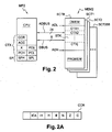
- FIG. 2 schematically represents a new generation 8-bit MP2 microprocessor, aimed by the plaintiff.
- the MP2 microprocessor stands out of the microprocessor MP1 by the fact that it includes a MEM2 extended memory plan addressable under 24 bits instead 16 bits, via the ADBUS address bus. So the plan memory MEM2 here comprises 256 sectors SCT0, SCT1, ... SCT255 of 64 KB each, and the first sector SCT0 corresponds to the MEM1 memory plane of the microprocessor MP1.
- the MP2 microprocessor be compatible with the MP1 microprocessor, i.e. that it can receive and execute programs application developed for the MP1 microprocessor.
- the space allocated to the STK stack must therefore remain constant is still delimited by the ADL, ADH addresses in the sector SCT0. Otherwise, if a change in the size and / or location of the battery microprocessor was planned, such a change could lead to program data encroachment and program application data designed for the MP1 microprocessor, on the battery location of the MP2 microprocessor.
- the size of the STK stack being kept constant, the forecast the PCE extended address register limits the number of nested programs since a byte of additional contextual data must be saved.
- the number of programs can be nested is now 25/6 or 4 at instead of 5 (one line of the STK stack remaining unused).
- the present invention aims, in particular, to overcome this disadvantage.
- an objective of the invention is to preserve the compatibility between two generations of microprocessors distinguished by an extension of the memory map and an extension of the counter size ordinal.
- a more general objective of the present invention is to provide a data backup process contextual to optimize the management of space allocated to the stack in order to maintain a degree high nesting of programs.
- a microprocessor comprising a central unit and a plan memory, the central unit comprising registers containing contextual data and a pointer to stack, the memory plan including a stack for the contextual data backup, central unit being arranged to save contextual data when switching from first to second program, with the particularity that the central unit is arranged to save contextual data contained in a variable number of registers which is function of the value of at least one flag stored in a register to save.
- the central unit is arranged to change the value of the flag accordingly the contents of a register, before saving contextual data contained in a variable number of registers which is a function of the value of the flag.
- the central unit is arranged to change the value of the flag accordingly the contents of an extended address register of a ordinal counter of the central unit.
- the central unit is designed for, when the content of the address register extended is 0, save all registers of the central unit containing contextual data to the exception of the extended address register, or when the content of the extended address register is not equal to 0, save all central unit registers containing contextual data including the extended address register.
- the central unit is arranged to carry out a test on the value of the flag to determine the number of registers to save.
- the central unit is arranged for, when returning to the first program, restore the register containing the flag and restore contextual data contained in a number registers variable which is a function of the value of flag present in the restored register.
- the central unit is arranged to save the register last containing the flag.
- the flag comprises at least one bit of a register containing flags of condition code.
- the invention also relates to a method of battery management of a microprocessor comprising a central unit and a memory map, the central unit including registers containing data contextual and a stack pointer, the stack being a memory area dedicated to data backup contextual when switching from first to second program, the method comprising saving contextual data contained in a variable number of registers which is a function of the value of at least one flag stored in a register to save.
- the method comprises a step of modifying the value of the flag in depending on the contents of a register, before saving contextual data contained in a number registers variable which is a function of the value of flag.
- the value of the flag is modified according to the content of a register of addressing an ordinal counter of the unit Central.
- the method comprises stages in which when the contents of the register of extended addressing is 0, save all central unit registers containing data contextual except for the address register extended, or when the content of the address register extended is not 0, save all central unit registers containing data contextual including the extended address register.
- the method comprises a stage of testing the value of the flag for determine the number of registers containing the data to save.
- the method comprises steps to restore the registry containing the flag and then restore contextual data contained in a variable number of registers which is function of the value of the flag present in the restored register.
- the register containing the flag is saved last and is restored on first.
- the flag is formed by at least one bit of a register containing flags of condition code.
- Figure 2 already described schematically the architecture of a memory plane microprocessor extended MP2 in which is implemented a method of STK stack management according to the invention.
- the PC ordinal counter here includes 24 bits stored in three bytes in PCE, PCH, PCL registers of the CPU.
- the extended memory plan MEM2 has 256 sectors SCT0 to SCT255 of 64 Kbytes each.
- the CPU is arranged to execute, in addition to a game new generation instructions to work on the whole extent of the memory plan, a game simplified instructions to work on the first sector SCT0, which retains the same structure that the MEM1 memory plane of the microprocessor First generation MP1 shown in Figure 1, so that the two generations of microprocessors are compatible.
- PCE extended addressing register of PC ordinal counter is reset and left at zero, since the instructions of the old programs generation are recorded in the first sector SCT0, whose addresses are coded only on 16 bits and can be managed using PCH registers, PCL.
- the new instruction set is however intended for programs recorded in all sectors SCT1 to SCT255 and uses the PCE register.
- the CPU which is conventionally a state machine wired logic or a microprogrammed logic machine, is designed to save contextual data present in the registers CCR, ACC, X, PCH, PCL, CPE according to a stack management method according to the invention.
- the CPU does not save the contents of the PCE extended addressing register when this one is zero.
- information indicating that whether the PCE extended address register has been saved is inserted in the contextual data so that the CPU knows, when restoring contextual data, what is the number of data to read from the STK stack.
- the code register CCR condition of the first MP1 microprocessor generation contains two available slots. Mon of these slots is used in the microprocessor MP2 to store an IEA flag whose value 1 or 0 forms the above information.
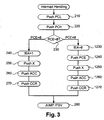
- FIG. 3 is a flowchart titled "Interrupt Handling Sequence " interruption) describing backup operations ("PUSH" instructions) of contextual data in the STK stack, executed by the CPU.
- the CPU first backups the PCL register and the PCH register in two stages 210 and 220. A the next step 230, the CPU tests the content of the PCE register.
- the CPU If the content of the PCE register is zero, the CPU puts the IEA flag at 1 in the condition code register CCR during a step 240. The CPU then executes steps 250, 260, 270 during which it saves successively the registers of index X, of accumulator ACC then CCR condition code (containing the IEA flag to 1), without saving the PCE register. The CPU is running then a step 280 "JUMP ITSV" ("Jump to Interrupt Service Routine ") jump to a runtime address of a interrupt processing routine provided by an interrupt vector.
- JUMP ITSV "Jump to Interrupt Service Routine "
- the CPU sets the IEA flag to 0 and executes steps 1240, 1250, 1260, 1270 in which it successively backs up the PCE, X, ACC and CCR (containing the IEA flag at 0).
- the CPU is running then step 280 "JUMP ITSV" jump to the subroutine interruption.
- FIG. 4 is a flowchart titled “Return from Interrupt”representing contextual data restore operations after execution of the interrupt routine.
- the CPU performs data recovery ("POP" instruction) in reverse order from their saving, according to the principle of stacking / unstacking LIFO, by destocking contextual data from the stack and restore registers starting with last data stored in the stack.
- POP data recovery
- step 310 the CPU restores first of all the registers CCR, ACC and X, successively.
- step 340 the CPU tests the value of the IEA flag in the CCR register, which was restored in step 310.
- the CPU clears the PCE extended program address register during a step 350, then restores the PCH and PCL registers of the PC ordinal counter in steps 360, 370.
- the CPU then executes a step 380 "JUMP PC" during which it jumps to the address contained in the counter ordinal PC as restored, to resume execution of the initial program.
- the CPU restores the three registers PCE, PCH and PCL of the counter ordinal in steps 1350, 1360, 1370, then goes to the jump step 380.
- Test step 340 may be an implicit step if the CPU is a wired logic state machine.
- the connection from step 330 to steps 350 or 1350 is a function of the IEA flag used as a bit acting on the transitions from one state to another of the state machine.
- the battery management method according to the invention thus ensures compatibility of the MP2 microprocessor with the programs developed on the first generation of MP1 microprocessor. With such programs, the content of the PCE registry is always null and the PCE register is never saved. The maximum number of nested subroutines is thus preserved and the risks of overflow of the stack are discarded.
- the PCE register is also not saved when its content is zero when executing a program developed using the new game instructions, which then optimizes the filling the stack, reduce the number of operations performed by the CPU for backup and restoring the context, winning a few cycles and speed up the processing of interruptions.
- the present invention is thus capable of various applications, regardless of the problem of compatibility between microprocessors.
- the fact that the PCE register is not saved when its content is zero saves space available in the stack and increase the number nesting of subprograms.
- This mechanism of conditional backup of a registry can by elsewhere be extended to other registers than the PCE register.
- FIG. 5 represents an MP3 microprocessor comprising, like the previous one, a central processing unit CPU and a memory plane MEM3 in which an area of fixed size forms the stack STK of the CPU.
- the CPU here includes any number of registers CR, R1, R2, ... R M-1 , R M , ... R M + N-1 , for example 8-bit registers, containing contextual data.
- the CPU also includes registers SPH, SPL containing the two bytes of the stack pointer SP.
- the registers CR, R1 to R M-1 contain contextual data of essential type and the registers R M to R M + N-1 contain contextual data of non-essential type, likely to be not used by an application program.
- a particular register here the register CR, is dedicated to the storage of an ISV flag accessible for reading and writing to the user of the microprocessor, that is to say accessible to the application program developed by the user.
- the value of the ISV flag is checked by the application program to vary the number of registers saved when switching to a subroutine.
- FIG. 6 is a flowchart titled "Interrupt Handling"representing stages of saving contextual data executed by the CPU in response to an interrupt signal.
- the CPU tests the state of the ISV flag contained in the CR register.
- the CPU executes a series 520 of steps of saving in the stack STK the content of M registers, here the registers R1, R2, ... R M-1 , CR, the register CR being saved last.
- M bytes of contextual data are saved and the stack pointer is incremented by M.
- the CPU then performs a step 540 "JUMP ITSV"("Jump to Interrupt Service Routine") to jump to an address supplied by a vector of interrupt, for executing an interrupt processing routine.
- the CPU executes a series 530 of steps of saving in the stack STK of the whole of the M + N registers R1, R2, .. R M-1 , R M , ... R M + N-1 , CR, the CR register being saved last.
- M + N bytes of contextual data are saved and the stack pointer is incremented by M + N.
- the CPU goes to jump step 540, to execute the interrupt routine.
- Figure 7 is a flowchart titled “Return from Interrupt” illustrating the restoration steps CPU registers when returning to the program initial.
- the CPU first restores the CR register during a step 610.
- the CPU then tests during of a step 620 the ISV flag present in the register restored.
- the CPU executes a series 630 of steps for restoring the registers R M-1 , ... R2, R1, by discharging the following M-1 bytes from the stack. Then, during a step 650 "JUMP PC", the CPU jumps to the address contained in the ordinal counter PC to resume execution of the initial program.
- the CPU executes a series 640 of steps to restore the registers R M + N + 1 , ... R M , R M-1 , ... R2, R1, by discharging stacks the following M + N-1 bytes, then goes to jump step 650.
- test step 620 can also be implicit if the CPU is a state machine with logic cable.
- the connection from step 610 to step 630 or to step 640 is then determined by the ISV flag in as bit acting on the state transitions of the state machine.
- Conditional backup and restore according to the invention may also relate to several groups of registers if an indicator with several flags is provided.
- a two indicator flags ISF1, ISF2 allows to define 4 configurations different backup, and define four groups different registers to save, the registers containing essential contextual data being included in each of the register groups.
- microprocessor is in no way limiting, this invention generally applicable to any type of integrated circuit comprising a central unit for run programs, including data contextual to save when switching a another program, such as microcontrollers, DSPs (signal processing processors), etc.
- the implementation of the process of the invention is thus particularly advantageous in microcontrollers which due to the various peripherals that they include, must process queues long, pending interruptions, requiring a high degree of nesting of the subprograms interruption.
- the present invention allows then optimize the stack management in order to maximize the degree of nesting.
Landscapes
- Engineering & Computer Science (AREA)
- Software Systems (AREA)
- Theoretical Computer Science (AREA)
- Physics & Mathematics (AREA)
- General Engineering & Computer Science (AREA)
- General Physics & Mathematics (AREA)
- Executing Machine-Instructions (AREA)
Abstract
Description
- la figure 1 précédemment décrite représente sous forme de bloc l'architecture d'un microprocesseur classique,
- la figure 1A représente le contenu d'un registre du microprocesseur de la figure 1,
- la figure 2 représente sous forme de bloc l'architecture d'un microprocesseur selon l'invention, ayant un plan mémoire étendu,
- la figure 2A représente le contenu d'un registre du microprocesseur de la figure 2,
- la figure 3 est un organigramme représentant des étapes d'empilement de données selon un procédé de gestion de pile selon l'invention,
- la figure 4 est un organigramme représentant des étapes de dépilement de données selon le procédé de gestion de pile selon l'invention,
- la figure 5 représente l'architecture d'un microprocesseur comprenant un nombre quelconque de données contextuelles, et illustre une généralisation du procédé de l'invention à un tel microprocesseur,
- la figure 6 est un organigramme représentant des étapes d'empilement de données selon une variante du procédé de gestion de pile selon l'invention, et,
- la figure 7 est un organigramme représentant des étapes de dépilement de données selon la variante du procédé de gestion de pile selon l'invention.
- si ISV=0, sauvegarde du registre CR puis sauvegarde des registres R1 à RM-1, ou
- si ISV=1, sauvegarde des registres RM à RM+N-1, puis sauvegarde du registre CR, puis sauvegarde des registres R1 à RM-1.
- restauration des registres R1 à RM-1,
- restauration du registre CR,
- si ISV=1, restauration des registres RM à RM+N-1.
Claims (16)
- Microprocesseur (MP2, MP3) comprenant une unité centrale (CPU) et un plan mémoire (MEM2, MEM3), l'unité centrale comprenant des registres (CCR-PCL...CR-RM+N-1) contenant des données contextuelles (CTX) et un pointeur de pile (SP, SPH, SPL), le plan mémoire comprenant une pile (STK) pour la sauvegarde de données contextuelles (CTX1-CTXj), l'unité centrale étant agencée pour sauvegarder des données contextuelles lors d'un basculement d'un premier à un second programme,
caractérisé en ce que l'unité centrale est agencée pour sauvegarder des données contextuelles contenues dans un nombre variable de registres qui est fonction de la valeur d'au moins un drapeau (IEA, ISV) stocké dans un registre (CCR, CR) à sauvegarder. - Microprocesseur selon la revendication 1, dans lequel l'unité centrale (CPU) est agencée pour modifier la valeur du drapeau (IEA) en fonction du contenu d'un registre (PCE), avant de sauvegarder des données contextuelles contenues dans un nombre variable de registres qui est fonction de la valeur du drapeau (IEA).
- Microprocesseur selon la revendication 2, dans lequel l'unité centrale est agencée pour modifier la valeur du drapeau (IEA) en fonction du contenu d'un registre d'adressage étendu (PCE) d'un compteur ordinal (PC) de l'unité centrale.
- Microprocesseur selon la revendication 3, dans lequel l'unité centrale est agencée pour :quand le contenu du registre d'adressage étendu est égal à 0, sauvegarder tous les registres de l'unité centrale contenant des données contextuelles à l'exception du registre d'adressage étendu (PCE), ou,quand le contenu du registre d'adressage étendu n'est pas égal à 0, sauvegarder tous les registres de l'unité centrale contenant des données contextuelles y compris le registre d'adressage étendu (PCE).
- Microprocesseur selon l'une des revendications 1 à 4, dans lequel l'unité centrale est agencée pour effectuer un test sur la valeur du drapeau (ISV, IEA) afin de déterminer le nombre de registres à sauvegarder.
- Microprocesseur selon l'une des revendications 1 à 5, dans lequel l'unité centrale est agencée pour, lors du retour au premier programme :restaurer le registre (CCR, CR) contenant le drapeau (IEA, ISV) et,restaurer des données contextuelles contenues dans un nombre variable de registres qui est fonction de la valeur du drapeau (IEA, ISV) présent dans le registre restauré.
- Microprocesseur selon l'une des revendications 1 à 6, dans lequel l'unité centrale est agencée pour sauvegarder en dernier le registre (CCR, CR) contenant le drapeau (IEA, ISV).
- Microprocesseur selon l'une des revendications 1 à 7, dans lequel le drapeau (IEA) comprend au moins un bit d'un registre (CCR) contenant des drapeaux de code condition.
- Procédé de gestion de la pile (STK) d'un microprocesseur (MP2, MP3) comprenant une unité centrale (CPU) et un plan mémoire (MEM2, MEM3), l'unité centrale comprenant des registres (CCR-PCL ... CR-RM+N-1) contenant des données contextuelles (CTX) et un pointeur de pile (SP), la pile (STK) étant une zone du plan mémoire dédiée à la sauvegarde de données contextuelles lors d'un basculement d'un premier à un second programme,
caractérisé en ce qu'il comprend la sauvegarde de données contextuelles contenues dans un nombre variable de registres qui est fonction de la valeur d'au moins un drapeau (IEA, ISV) stocké dans un registre (CCR, CR) à sauvegarder. - Procédé selon la revendication 9, comprenant une étape de modification de la valeur du drapeau (IEA) en fonction du contenu d'un registre (PCE), avant la sauvegarde de données contextuelles contenues dans un nombre variable de registres qui est fonction de la valeur du drapeau (IEA).
- Procédé selon la revendication 10, dans lequel la valeur du drapeau (IEA) est modifiée en fonction du contenu d'un registre d'adressage étendu (PCE) d'un compteur ordinal (PC) de l'unité centrale.
- Procédé selon la revendication 11, comprenant les étapes suivantes :quand le contenu du registre d'adressage étendu est égal à 0, sauvegarder tous les registres de l'unité centrale contenant des données contextuelles à l'exception du registre d'adressage étendu (PCE), ou,quand le contenu du registre d'adressage étendu n'est pas égal à 0, sauvegarder tous les registres de l'unité centrale contenant des données contextuelles y compris le registre d'adressage étendu (PCE).
- Procédé selon l'une des revendications 9 à 12, comprenant une étape de test de la valeur du drapeau (ISV, IEA) pour déterminer le nombre de registres contenant les données à sauvegarder.
- Procédé selon l'une des revendications 9 à 13, comprenant les étapes suivantes:restauration du registre (CCR, CR) contenant le drapeau (IEA, ISV), puis,restauration de données contextuelles contenues dans un nombre variable de registres qui est fonction de la valeur du drapeau (IEA, ISV) présent dans le registre restauré.
- Procédé selon l'une des revendications 9 à 14, dans lequel le registre (CCR, CR) contenant le drapeau (IEA, ISV) est sauvegardé le dernier et est restauré le premier.
- Procédé selon l'une des revendications 9 à 15, dans lequel le drapeau (IEA) est formé par au moins un bit d'un registre (CCR) contenant des drapeaux de code condition.
Applications Claiming Priority (2)
| Application Number | Priority Date | Filing Date | Title |
|---|---|---|---|
| FR0301879 | 2003-02-17 | ||
| FR0301879A FR2851349A1 (fr) | 2003-02-17 | 2003-02-17 | Procede de gestion d'une pile de microprocesseur pour la sauvegarde de donnees contextuelles |
Publications (2)
| Publication Number | Publication Date |
|---|---|
| EP1447747A1 true EP1447747A1 (fr) | 2004-08-18 |
| EP1447747B1 EP1447747B1 (fr) | 2007-08-01 |
Family
ID=32669384
Family Applications (1)
| Application Number | Title | Priority Date | Filing Date |
|---|---|---|---|
| EP04000574A Expired - Lifetime EP1447747B1 (fr) | 2003-02-17 | 2004-01-14 | Procédé de gestion d'une pile de microprocesseur pour la sauvegarde de données contextuelles |
Country Status (4)
| Country | Link |
|---|---|
| US (1) | US7421570B2 (fr) |
| EP (1) | EP1447747B1 (fr) |
| DE (1) | DE602004007835T2 (fr) |
| FR (1) | FR2851349A1 (fr) |
Cited By (1)
| Publication number | Priority date | Publication date | Assignee | Title |
|---|---|---|---|---|
| RU2340933C2 (ru) * | 2006-10-19 | 2008-12-10 | Общество с ограниченной ответственностью "Юникор микросистемы" | Способ переключения контекста вычислительного процесса при прерывании программы или переходе к подпрограмме |
Families Citing this family (5)
| Publication number | Priority date | Publication date | Assignee | Title |
|---|---|---|---|---|
| US20140013129A1 (en) | 2012-07-09 | 2014-01-09 | L. Pierre de Rochemont | Hybrid computing module |
| US20160381050A1 (en) | 2015-06-26 | 2016-12-29 | Intel Corporation | Processors, methods, systems, and instructions to protect shadow stacks |
| US10394556B2 (en) * | 2015-12-20 | 2019-08-27 | Intel Corporation | Hardware apparatuses and methods to switch shadow stack pointers |
| US10430580B2 (en) | 2016-02-04 | 2019-10-01 | Intel Corporation | Processor extensions to protect stacks during ring transitions |
| KR20240027356A (ko) | 2022-08-23 | 2024-03-04 | 에스케이하이닉스 주식회사 | 데이터 보호 기능을 수행하는 데이터 저장 장치 및 프로그램 컨텍스트를 이용하여 데이터 보호 기능을 지원하는 호스트 장치 |
Citations (3)
| Publication number | Priority date | Publication date | Assignee | Title |
|---|---|---|---|---|
| US6205467B1 (en) * | 1995-11-14 | 2001-03-20 | Advanced Micro Devices, Inc. | Microprocessor having a context save unit for saving context independent from interrupt requests |
| WO2002013005A1 (fr) * | 2000-08-09 | 2002-02-14 | Advanced Micro Devices, Inc. | Uc ayant acces a un ensemble de registres etendus dans un mode registres etendus |
| US6367005B1 (en) * | 1998-04-21 | 2002-04-02 | Idea Corporation Of Delaware | System and method for synchronizing a register stack engine (RSE) and backing memory image with a processor's execution of instructions during a state saving context switch |
Family Cites Families (5)
| Publication number | Priority date | Publication date | Assignee | Title |
|---|---|---|---|---|
| US4445173A (en) * | 1981-09-11 | 1984-04-24 | Data General Corporation | Improved system for saving and restoring state in call and return operations |
| EP0942357A3 (fr) * | 1998-03-11 | 2000-03-22 | Matsushita Electric Industrial Co., Ltd. | Microprocesseur compatible avec une pluralité de formats d'instructions |
| US6408325B1 (en) * | 1998-05-06 | 2002-06-18 | Sun Microsystems, Inc. | Context switching technique for processors with large register files |
| US6205543B1 (en) * | 1998-12-03 | 2001-03-20 | Sun Microsystems, Inc. | Efficient handling of a large register file for context switching |
| US7210026B2 (en) * | 2002-06-28 | 2007-04-24 | Sun Microsystems, Inc. | Virtual register set expanding processor internal storage |
-
2003
- 2003-02-17 FR FR0301879A patent/FR2851349A1/fr not_active Withdrawn
-
2004
- 2004-01-14 DE DE602004007835T patent/DE602004007835T2/de not_active Expired - Fee Related
- 2004-01-14 EP EP04000574A patent/EP1447747B1/fr not_active Expired - Lifetime
- 2004-02-17 US US10/779,855 patent/US7421570B2/en not_active Expired - Lifetime
Patent Citations (3)
| Publication number | Priority date | Publication date | Assignee | Title |
|---|---|---|---|---|
| US6205467B1 (en) * | 1995-11-14 | 2001-03-20 | Advanced Micro Devices, Inc. | Microprocessor having a context save unit for saving context independent from interrupt requests |
| US6367005B1 (en) * | 1998-04-21 | 2002-04-02 | Idea Corporation Of Delaware | System and method for synchronizing a register stack engine (RSE) and backing memory image with a processor's execution of instructions during a state saving context switch |
| WO2002013005A1 (fr) * | 2000-08-09 | 2002-02-14 | Advanced Micro Devices, Inc. | Uc ayant acces a un ensemble de registres etendus dans un mode registres etendus |
Cited By (1)
| Publication number | Priority date | Publication date | Assignee | Title |
|---|---|---|---|---|
| RU2340933C2 (ru) * | 2006-10-19 | 2008-12-10 | Общество с ограниченной ответственностью "Юникор микросистемы" | Способ переключения контекста вычислительного процесса при прерывании программы или переходе к подпрограмме |
Also Published As
| Publication number | Publication date |
|---|---|
| US7421570B2 (en) | 2008-09-02 |
| FR2851349A1 (fr) | 2004-08-20 |
| EP1447747B1 (fr) | 2007-08-01 |
| DE602004007835D1 (de) | 2007-09-13 |
| US20040221141A1 (en) | 2004-11-04 |
| DE602004007835T2 (de) | 2008-04-10 |
Similar Documents
| Publication | Publication Date | Title |
|---|---|---|
| AU2010247785B2 (en) | Displaying transition images during a slide transition | |
| EP1447747B1 (fr) | Procédé de gestion d'une pile de microprocesseur pour la sauvegarde de données contextuelles | |
| EP3182292A1 (fr) | Procédé de prédiction d'une donnée a précharger dans une mémoire cache | |
| FR2822260A1 (fr) | Procedes et dispositifs pour accelerer le temps de calcul d'un produit de montgomery d'un multiplication et d'une exponentiation modulaire | |
| FR2621719A1 (fr) | Procede de conversion d'adresse | |
| EP2585931A1 (fr) | Dispositif, chaine et procédé de traitement de données, et programme d'ordinateur correspondant | |
| EP0838053B1 (fr) | Procede et dispositif permettant a un programme fige de pouvoir evoluer | |
| FR2850179A1 (fr) | Dispositif d'antememoire pour un processeur de signal numerique et procede de commande | |
| FR2801693A1 (fr) | Procedes et appareils pour detecter la presence eventuelle d'exceptions | |
| CN101526921B (zh) | 写入数据的方法及装置 | |
| EP1881404A1 (fr) | Procédé de protection dynamique des données lors de l'exécution d'un code logiciel en langage intermédiaire dans un appareil numérique | |
| EP0733977B1 (fr) | Système informatique avec mémoires hiérarchisées | |
| FR3142592A1 (fr) | Mémoire non volatile | |
| EP3814893B1 (fr) | Accès mémoire de processeurs | |
| EP1436694A1 (fr) | Microprocesseur disposant d'un espace adressable etendu | |
| WO2017137675A1 (fr) | Instruction combinée d'addition et de vérification de bornes | |
| FR2896601A1 (fr) | Dispositif de traitement en notation polonaise inversee, et circuit integre electronique comprenant un tel dispositif de traitement. | |
| CN114546270B (zh) | 数据存储方法、装置及电子设备 | |
| CN1202653A (zh) | 存储器读取加速方法 | |
| CN115617276B (zh) | 一种数据存储方法及装置 | |
| JPH06231114A (ja) | 多体問題用計算装置及び計算方法 | |
| KR100333646B1 (ko) | 동영상 전문가 그룹 오디오 레이어 3 디코더의 입력 버퍼 | |
| EP1211599A1 (fr) | Microprocesseur comprenant des moyens de sauvegarde de données contextuelles lors d'un basculement dans un programme de test | |
| EP3814923A1 (fr) | Architecture de processeur asynchrone | |
| WO2021058773A1 (fr) | Procédé et calculateur de gestion d'échanges de données entre une pluralité de tâches |
Legal Events
| Date | Code | Title | Description |
|---|---|---|---|
| PUAI | Public reference made under article 153(3) epc to a published international application that has entered the european phase |
Free format text: ORIGINAL CODE: 0009012 |
|
| AK | Designated contracting states |
Kind code of ref document: A1 Designated state(s): AT BE BG CH CY CZ DE DK EE ES FI FR GB GR HU IE IT LI LU MC NL PT RO SE SI SK TR |
|
| AX | Request for extension of the european patent |
Extension state: AL LT LV MK |
|
| RAP1 | Party data changed (applicant data changed or rights of an application transferred) |
Owner name: STMICROELECTRONICS SA |
|
| 17P | Request for examination filed |
Effective date: 20050121 |
|
| AKX | Designation fees paid |
Designated state(s): DE FR GB IT |
|
| RBV | Designated contracting states (corrected) |
Designated state(s): DE FR GB IT |
|
| GRAP | Despatch of communication of intention to grant a patent |
Free format text: ORIGINAL CODE: EPIDOSNIGR1 |
|
| GRAS | Grant fee paid |
Free format text: ORIGINAL CODE: EPIDOSNIGR3 |
|
| GRAA | (expected) grant |
Free format text: ORIGINAL CODE: 0009210 |
|
| AK | Designated contracting states |
Kind code of ref document: B1 Designated state(s): DE FR GB IT |
|
| REG | Reference to a national code |
Ref country code: GB Ref legal event code: FG4D Free format text: NOT ENGLISH |
|
| REF | Corresponds to: |
Ref document number: 602004007835 Country of ref document: DE Date of ref document: 20070913 Kind code of ref document: P |
|
| GBT | Gb: translation of ep patent filed (gb section 77(6)(a)/1977) |
Effective date: 20071031 |
|
| PGFP | Annual fee paid to national office [announced via postgrant information from national office to epo] |
Ref country code: GB Payment date: 20071227 Year of fee payment: 5 |
|
| PGFP | Annual fee paid to national office [announced via postgrant information from national office to epo] |
Ref country code: DE Payment date: 20080115 Year of fee payment: 5 |
|
| PLBE | No opposition filed within time limit |
Free format text: ORIGINAL CODE: 0009261 |
|
| STAA | Information on the status of an ep patent application or granted ep patent |
Free format text: STATUS: NO OPPOSITION FILED WITHIN TIME LIMIT |
|
| 26N | No opposition filed |
Effective date: 20080506 |
|
| PGFP | Annual fee paid to national office [announced via postgrant information from national office to epo] |
Ref country code: FR Payment date: 20080131 Year of fee payment: 5 |
|
| GBPC | Gb: european patent ceased through non-payment of renewal fee |
Effective date: 20090114 |
|
| PG25 | Lapsed in a contracting state [announced via postgrant information from national office to epo] |
Ref country code: DE Free format text: LAPSE BECAUSE OF NON-PAYMENT OF DUE FEES Effective date: 20090801 |
|
| REG | Reference to a national code |
Ref country code: FR Ref legal event code: ST Effective date: 20091030 |
|
| PG25 | Lapsed in a contracting state [announced via postgrant information from national office to epo] |
Ref country code: GB Free format text: LAPSE BECAUSE OF NON-PAYMENT OF DUE FEES Effective date: 20090114 |
|
| PG25 | Lapsed in a contracting state [announced via postgrant information from national office to epo] |
Ref country code: FR Free format text: LAPSE BECAUSE OF NON-PAYMENT OF DUE FEES Effective date: 20090202 |
|
| PG25 | Lapsed in a contracting state [announced via postgrant information from national office to epo] |
Ref country code: IT Free format text: LAPSE BECAUSE OF NON-PAYMENT OF DUE FEES Effective date: 20080131 |